Transcription
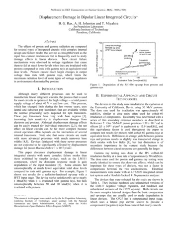
Published in IEEE Transactions on Nuclear Science, 46(6), 1660 (1999)Displacement Damage in Bipolar Linear Integrated Circuits†B. G. Rax, A. H. Johnston and T. MiyahiraJet Propulsion LaboratoryCalifornia Institute of TechnologyPasadena, CaliforniaAbstractI. INTRODUCTIONAlthough many different processes can be used tomanufacture linear integrated circuits, the process that is usedfor most circuits is optimized for high voltage -- a total powersupply voltage of about 40 V -- and low cost. This process,which has changed little during the last twenty years, useslateral and substrate pnp transistors that are available withinthe normal processing steps required for npn transistors.These pnp transistors have very wide base regions [1],increasing their sensitivity to displacement damage fromelectrons and protons. Although displacement damage effectscan be easily treated for individual transistors [2,3], the neteffect on linear circuits can be far more complex becausecircuit operation often depends on the interaction of severalinternal transistors. Note also that some circuits are madewith more advanced processes with much narrower basewidths [4,5]. Devices fabricated with these newer processesare not expected to be significantly affected by displacementdamage for proton fluences below 1 x 10¹² p/cm2.This paper discusses displacement damage in linearintegrated circuits with more complex failure modes thanthose exhibited by simpler devices, such as the LM111comparator, where the dominant response mode is gaindegradation of the input transistor [6]. Some circuits failcatastrophically at much lower equivalent total dose levelscompared to tests with gamma rays. For example, Figure 1shows test results for a radiation-hardened op-amp with aJFET input stage. The device works satisfactorily up to nearly1 Mrad(Si) when it is irradiated with gamma rays, but failscatastrophically between 50 and 70 krad(Si) when it isirradiated with protons.--------†The research in this paper was carried out by the Jet Propulsion Laboratory,California Institute of Technology, under contract with the NationalAeronautics and Space Administration, Code AE, under the NASAMicroelectronics Space Radiation Effects Program (MSREP).100Input Offset Voltage (mV)The effects of proton and gamma radiation are comparedfor several types of integrated circuits with complex internaldesign and failure modes that are not as straightforward as theinput bias current mechanism that is frequently used to studydamage effects in linear devices.New circuit failuremechanisms were observed in voltage regulators that causethem to fail at much lower levels when they are irradiated withprotons compared to tests with gamma rays at equivalent totaldose levels. Protons caused much larger changes in outputvoltage than tests with gamma rays, which limits themaximum radiation level of some types of voltage regulatorsin environments dominated by protons.Linear technologyRH1056 op-amp(JFET input stage)10200 MeVprotons1Catastrophicfailure between50 and 70 kradCobalt-60gamma rays0.1Radiation level guaranteedby manufacturer0.01110100Equivalent Total Dose [krad(Si)]1000Figure 1. Degradation of the RH1056 op-amp from protons andgamma rays.II. EXPERIMENTAL APPROACH AND CIRCUITTECHNOLOGIESThe devices in this study were irradiated at the cyclotron atthe University of California, Davis, using 50 MeV protons.The dose rate used for irradiation was approximately 40rad(Si)/s, similar to dose rates often used for cobalt-60irradiation of components. Dosimetry was determined with aseries of thin secondary emission monitors, as described inReference 7. One 50-MeV proton produces 1.59 x 10⁻⁷ rad insilicon [(1 x 10¹¹ p/cm2 is equivalent to 15.9 krad(Si)], andthis equivalence factor is used throughout the paper tocompare test results for protons with cobalt-60 gamma rays atequivalent levels. Differences in charge yield between gammarays and protons results in slightly less transported charge inthick oxides with low fields [8], but that distinction is ofsecondary importance in the current study because thedifferences between circuit response are generally far larger.Gamma ray testing was done at the JPL colbalt-60irradiation facility at a dose rate of approximately 50 rad(Si)/s.The dose rates used for proton and gamma ray testing werenearly identical to ensure that dose-rate effects, which can beimportant for these types of devices, was not a factor incomparisons between the two environments.Electricalmeasurements were made with an LTS2020 integrated circuittest system and a Hewlett-Packard 4156 parameter analyzer.The devices that were selected for the study are shown inTable 1. They include hardened and unhardened versions ofthe LM137 negative voltage regulator, and hardened andunhardened versions of the OP27 op-amp. Both circuits usefar more complex internal designs than the basic comparatorsand op-amps that are usually used to study degradation inlinear devices. The OP27 has a compensated input stage,which uses a lateral pnp current source to provide acompensated (negative) input bias current that nearly cancels
Published in IEEE Transactions on Nuclear Science, 46(6), 1660 (1999)Table 1. Devices Selected for Proton TestingManuf.CommentsOp-ampOp-ampOp-ampVoltage reg.Voltage reg.Voltage reg.Voltage reg.Anal. Dev.Lin. Tech.Lin. Tech.NationalNationalLinear Tech.Lin. Tech.Hardened devicePositive reg.Negative reg.Negative reg.Hardened devicethe positive input bias current required by the npn inputtransistor, as shown in Figure 2. Although this reduces theinput bias current, it causes circuit operation to depend on thebalance of this compensation scheme, which involves severaldifferent types of transistors.VCCLateral pnpcurrent sourcecompensatesinput base currentof npn transistors0050 MeV Unhardened(catastrophicfailure above2x1011 p/cm2)-0.0151.54x10116x1011Change in Output Voltage (% )OP-27OP-27RH-27LM117LM137LM137RH137FunctionChange in Output Voltage (V)Device2.0Proton Fluence (p/cm2)Figure 3. Effect of proton irradiation on output voltage degradationof hardened and commercial versions of the LM137 voltageregulator.As shown in Figure 4, the unhardened LM137 devicescontinue to function with moderate output degradation up to50 krad(Si) when they are tested with cobalt-60 gamma rays[the devices continue to function at 100 krad(Si)]. However, adifferent failure mechanism comes into play when the devicesare irradiated with protons which causes catastrophic failure.For the particular unit shown in Figure 4 catastrophic failureoccurred between 24 and 28 krad(Si); the shaded region showsthe range of failure levels observed for 8 different units fromthe same date code. Note that the spread in failure levels wasabout a factor of two.InputsVEEFigure 2. Simplified diagram of the compensated input stage used inthe OP-17 op-amp.The hardened process from Linear Technology is designedto withstand ionization damage, using a proprietary methodfor oxide growth. The process uses lateral and substrate pnptransistors that are physically similar to lateral and pnptransistors in conventional (unhardened) processes. The pnpstructures in both the hardened and unhardened processes areinherently sensitive to displacement damage because of therelatively wide base regions.III. EXPERIMENTAL RESULTSA. LM137 Negative Voltage RegulatorOutput voltage is one of the key parameters for voltageregulators, and most voltage regulators rely on bandgapreference circuits with npn transistors [7]. Figure 3 comparesthe output voltage degradation of the commercial andhardened LM137 voltage regulators when they are tested withprotons. Both device types exhibit similar changes in thatparameter. However, the commercial device stops functioningat about 2 x 10¹¹ p/cm2; the failure is catastrophic and doesnot recover even after extended time periods.Change in Output Voltage (%)2Range ofcatastrophicfailure levelswith protonrradiation1.5Catastrophicfailure betweenthese levels150 MeVProtons0.5Cobalt-60gamma rays005101520253035404550Total Dose [krad(Si)]Figure 4. Change in output voltage of unhardened LM137 regulatorswhen they are irradiated with protons and gamma rays.Special input/output measurements were made tocharacterize this mechanism. Figure 5 shows how the transfercharacteristics of the unhardened LM137 changed after protonirradiation. The curve labeled “0” shows the preirradiationbehavior. The output voltage begins to increase even at verylow input voltages, but there is a slight nonlinearity at about0.8 to 0.9 V. This nonlinear region occurs when the start-upcircuitry begins to operate. Preirradiation values of the startup
Published in IEEE Transactions on Nuclear Science, 46(6), 1660 (1999)voltage defined by that nonlinearity ranged from 0.9 to 1.45 Vfor different units. As the input voltage increases, the outputvoltage continues to increase until it reaches the cut-in voltage(2.7 V) at which point the output regulates to a very precisevoltage level.21.5The changes in start-up conditions after various levels ofproton irradiation are shown for several devices in Figure 6.The start-up voltage increases in a smooth, regular way as theradiation level increases. However, there are substantialdifferences in the radiation level at which catastrophic failureoccurs. Note that only small changes occurred when one ofthe devices was irradiated with gamma rays; the startup failuremode does not occur with gamma rays, only with protons.Vout 1.25V inregulationSuccessive protonirradiations causestart-up voltage toincrease1Cut-in voltage(typically 2.7 V)Unirradiated0.5000Equivalent Total Dose [krad(Si)]211234Voltage Applied to Input Pin (V)35Figure 5. Input output characteristics of the unhardened LM137voltage regulator before and after two proton irradiation levels.After the first irradiation level (5 x 10¹⁰ p/cm2), the outputvoltage no longer responds to the input voltage until it reachesapproximately 1.3 V. At that point there is an abrupt increasein output voltage, and for voltages above that transition pointthe circuit behaves much like it did prior to irradiation. Itcontinues to operate for input voltages above the cut-involtage, with only about a 1% change in the regulated outputvoltage compared to the preirradiation level.After the second irradiation level (1 x 10¹¹ p/cm2), theabrupt transition voltage condition has increased to 2.3 V.The output voltage remains stuck at zero volts until the inputvoltage increases above that value, at which point the devicebegins to operate normally.After the third irradiation to 1.5 x 10¹¹ p/cm2 the device nolonger functions, and the circuit will not operate even whenthe input voltage is raised to 40 V. From these measurements,it is clear that the minimum input voltage required to cause thedevice to operate has increased to a level above the cut-involtage, and the device has failed catastrophicallyA similar characterization method was used by Beaucour,et al., in a study of dose-rate effects of the LM137 [9].However, there is an important difference in our results withprotons. Beaucour, et al. showed that for ionization damagethe devices that he studied would eventually start to regulate ifthe input voltage was increased beyond the “new” start-upvoltage condition that occurred after irradiation.Consequently, the increase in start up voltage in their testswould only be important for applications with very lowinput/output voltage conditions.†--------†Beaucour, et al. did not identify the specific manufacturers of the LM137devices that they tested in their study, and it is possible that the devices forwhich the startup conditions changed were from a different manufacturer.0168243240Cut-In VoltageVoltage to Start Internal RegulatorOutput Voltage (V)Device fails once start-upvoltage reaches cut-involtageThe characteristics of the National LM137 were markedlydifferent when they were irradiated with protons. After thestart-up voltage degraded to the point where it exceeded thecut-in voltage, the device could not be made to operate evenwhen the input voltage was raised to the maximum inputvoltage level. Thus, failure will occur even in applicationswith high input/output voltage “headroom.”Catastrophic2.5 failure occurs whenstart-up voltage reachescut-in voltage21.51Typical resultswith cobalt-60gamma rays0.5National LM13750 MeV protons005x10101x10111.5x10112x10112.5x1011Proton Fluence (p/cm2)Figure 6. Dependence of start-up voltage on proton fluence for fivedevices illustrating the range of failure levels.LM137 devices from Linear Technology (LT137) werealso evaluated in this way. The LT137 parts did not show anyevidence of the start-up failure mechanism observed for theNational version of the part, even when tested at levels up tonearly 1012 p/cm2. The parts from Linear Technology alsoexhibited smaller changes in output voltage compared to theparts made by National. This illustrates that the importanceof proton damage can vary by a large amount betweendifferent manufacturers. In this case the parts from LinearTechnology are far less affected by ionization damage (cobalt60 tests) compared to parts from the other vendor. Protondamage produces a combination of displacement andionization damage, and the reason for this difference may bedue more to that difference than in differences in thesensitivity of internal parts to displacement damage.
Published in IEEE Transactions on Nuclear Science, 46(6), 1660 (1999)B. LM117 Positive Voltage RegulatorC. OP-27 Operational AmplifiersProton and cobalt-60 tests were also done on the LM117, apositive regulator. The LM117 showed some evidence of thesame start-up failure mechanism exhibited by the LM137, asshown in Figure 7. However, the effect did not becomesignificant until much higher radiation levels were reached.Proton tests were also done for the OP27 and RH27 opamps. These devices use the compensated input stagedescribed previously in Figure 2, employing a current source(with a multiple-collector pnp transistor) to provide a“bucking” current for the input current of the npn transistor ateach input. As shown in Figure 9, the OP27 and RH27devices continued to operate at high levels, even above100 krad(Si) [equivalent total dose] when they were irradiatedwith protons. This is an interesting contrast with the RH1056result, where a hardened device failed catastrophically atlevels well below the design specification value when it wasirradiated with protons (see Figure 1).National SemiconductorStart-Up Voltage (V)4350 MeV Protons2Cobalt-60 gamma rays10020406080100Equivalent Total Dose [krad(Si)]120140Figure 7. Dependence of start-up voltage on equivalent levels ofprotons and gamma rays for the National LM117 voltage regulator.One important difference was observed for the LM117.Much larger changes in output voltage occurred for that partcompared to the LM137. These results are shown in Figure 8.With protons, the change in output voltage at equivalentradiation levels is about five times larger for the LM117compared to the LM137 (see Figure 4 for the LM137 results).The changes in reference voltage observed for the LM117 arealso substantially higher than the typical voltage changesexhibited by conventional bandgap reference circuits [8]. Theunusually large changes that occur for this circuit arepotentially important in many applications, even though thestart-up mechanism is not a factor for that particular devicedesign.Change in Output Voltage (V)05% change in voltage50 MeV ProtonsNominal initial voltage 1.25 volts(bandgap reference)020406080100Equivalent Total Dose [krad(Si)]Hardened part (RH27)0-100120Biasedcommercialpart (OP27)-200-300Unbiasedcommercialpart (OP27)-400-50050 MeV Protons01x10112x1011 3x10¹¹ 4x10¹¹Proton Fluence (p/cm2)5x10116x1011Figure 9. Degradation of input bias current of unhardened andhardened versions of the OP27 op-amp. The RH27 is made with aspecial process by Linear Technology; the OP27 is made with acommercial process by Analog Devices.-0.1-0.15100-600Cobalt-60 gamma rays-0.05Note however that there are very large increases in inputbias current for the commercial OP27 devices that were notobserved for the hardened version of the part. These changes,which were always in the negative direction, occur becausethe lateral pnp compensation stage no longer operatesproperly. It overcompensates, causing very large negativeinput currents at both the inverting and noninverting inputs.However, other circuit parameters such as input offset voltage,open-loop gain and output drive current are only slightlydegraded.Note also that considerably more degradationoccurs when the commercial devices are irradiated withoutbias compared to the results under bias. This suggests thationization damage is the main reason for the degradation, notdisplacement damage, because displacement damage is notaffected by bias conditions during irradiation.Change in Input Bias Current (nA)5140Figure 8. Dependence of the output voltage of the National LM117on proton fluence.Tests were also done on commercial parts manufacturedby a different vendor, Linear Technology. Results for theLT27 were quite different than the results for the commercialOP27 from Analog Devices. As shown in Figure 10, the inputbias current of the Linear Technology version of the partincreased in the positive direction (implying that the currentsource is turning off, undercompensating the input stage),exactly opposite to the behavior of the OP27 in Figure 9.
Published in IEEE Transactions on Nuclear Science, 46(6), 1660 (1999)Input Bias Current (nA)30050 MeV Protons200Cobalt-60 Gamma Rays1000050100150Equivalent Total dose [krad (Si)]Figure 10. Degradation of input bias current of the LT27 op-ampfrom Linear Technology showing opposite behavior to that of theOP27.IV. DISCUSSIONBecause wide-base pnp transistors are sensitive todisplacement damage, protons will always cause more damageto occur from protons in these structures compared to thedamage produced by equivalent total dose levels from gammarays. The npn transistors used in typical linear integratedcircuits have much narrower base regions, and are relativelyinsensitive to displacement damage effects. The net effect ofdisplacement damage at the circuit level depends on thedetails of the circuit design. Many linear integrated circuitsare designed to tolerate wide variations in the gain of internalpnp transistors, and for such circuits the increase in damagefrom displacement effects may be unimportant.In cases where substantial degradation occurs fromionization damage (note the LM111 reported in reference 6),the net impact of the increased displacement damage may beslight. However, for circuits like the RH1056 and LM137,displacement damage causes catastrophic failure to occur, andthe circuit failure appears to be the result of mechanisms thatdo not occur during tests in ionization environments, evenwhen the tests are carried out at very high levels. This type ofcatastrophic failure is of extreme concern for spaceapplications, and illustrates the need to test linear integratedcircuits in proton environments.Using data in the literature to determine doping levels andbase width [11,12], it is possible to calculate the nominal gainand resulting effects from displacement damage for substrateand lateral pnp transistors. The Messenger-Spratt equationwas used, increasing the damage constant by a factor of 2.2 tocorrect for the increased non-ionizing energy loss factor for 50MeV protons [14]. These results are shown in Figure 11. Theresults are in close agreement with earlier circuit results forLM111 comparators from National Semiconductor, butslightly overestimate the displacement damage in LM111devices made by Analog Devices [6]. It shows that evenlateral pnp transistors retain a substantial amount of theirinitial gain at equivalent total dose levels of 40-50 krad(Si)when one considers only displacement damage.Notehowever that lateral pnp transistors with “split collectors” -typically used in current sources -- will undergo considerablyGain Degradation Due to Displacement Damagemore degradation because all of the base current flows intoonly a single section of the split device [1]. Thus, changes incurrent source values of 10-20% can occur at those radiationlevels when current sources are used, even withoutconsidering the additional damage from ionization, which isnot included in the figure.400Proton Fluence (p/cm2 )1201 x 10112 x 10114 x 10113 x 10115 x 10116 x 101110052 MeV 0708090100Equivalent Total Dose [krad(Si)]Figure 11. Typical gain degradation from protons for substrate andlateral pnp transistors (equivalent total dose levels are shown).The issue of whether such changes are important dependson the circuit configuration. Note for example that protondisplacement damage causes much larger changes in theoutput reference voltage of the LM117 than in the LM137from the same manufacturer. This clearly has to be due todifferences in internal circuit design. The markedly differentresponse of the LT27 and OP27 op-amps is also indicative ofinternal design differences.In some cases failure modes depend on the detailed balance(or imbalance) of transistors in specific subcircuits, as shownby Barnaby et al. in their study of the LM117 at different doserates using gamma rays [9]. Similar issues could easily occurwhen proton damage is compared with ionization damage athigh dose rates if the particular circuit design relies onbalancing or matching of internal transistors of different types.This is the likely reason that the reference voltage of theLM117 is so much larger than that of the LM137 in ourproton tests on those two device types. Note also that bothionization and displacement damage effects are significant formost circuits. Thus, it is difficult to do separate testing withneutrons to determine how displacement damage will combinewith ionization damage at the circuit level, even though suchan approach would be very useful with discrete transistors ortest structures. It is also clear that simply doing ionizationtests at higher radiation levels (“overtesting’) cannot becounted on to bound the proton damage issue when differentfailure mechanisms are introduced by displacement damageeffects.-------†In our tests with gamma rays the LM117 reference voltage decreased, in theopposite direction compared to the results obtained by Barnaby, et al. [15].However, the reference voltage of conventional bandgap reference designs issensitive to slight mismatches in gain degradation and current matching, andcan change in either direction [10]. This is the likely reason for the differentresults between the two sets of data for the LM117. Note that the absolutechanges in voltage are relatively small.
Published in IEEE Transactions on Nuclear Science, 46(6), 1660 (1999)In principle, one could use neutrons as an alternative toproton testing, provided the neutron environment could beadjusted to provide equivalent ratios of ionization anddisplacement damage. However, protons produce two to threeorders of magnitude more ionization for equivalentdisplacement damage compared to a fast-burst reactor or otherhard neutron source. Although it is possible to degrade theneutron source to increase the relative ratio of ionization todisplacement damage, the inevitable result is severedegradation of the neutron spectrum with higher uncertaintyabout the effective value of the displacement damagecomponent. The advantage of using protons is that protonsare the dominant environment for many space systems, and50 MeV protons are near the peak in the proton energyspectrum for many applications.Proton testing is costly, and it is probably unnecessary toinclude proton tests for all space applications even whenprotons are the dominant source of ionization damage. Thetesting done to date suggests that displacement damage willonly be important for equivalent total dose levels above20 krad(Si), which is consistent with the calculated postradiation gain values in Figure 11. However, it is possible thatdevices operating at very low power or with very low internalvoltages could be affected at lower levels. Proton damage islikely to remain an important issue, particularly for new circuitdesigns that operate with low power and low voltages.V. CONCLUSIONSThis work has shown that proton displacement damage canintroduce different failure modes with catastrophic failure forsome circuit types. Such effects can occur in both hardenedand unhardened circuits. The reasons for such failures arecomplex, and depend on the internal design and margin forgain degradation. Catastrophic failure in voltage regulators isespecially important because their failure can impact theoperation of key subcircuit elements. It is important torecognize the importance of these effects and to includeproton testing for certain types of linear integrated circuits.Proton damage is a complex issue, made still moredifficult by the large number of ways that transistors withdisplacement damage sensitivity can be used in circuitdesigns. Many circuit-level effects are inherently nonlinear,with failure modes that only surface after the internal gain of acritical transistor falls below the minimum value for thecircuit. These characteristics can vary widely, even betweendifferent units from the same process, as shown by the LM137catastrophic failure mechanism. This may make it necessaryto evaluate proton damage effects on a lot-by-lot basis forsome circuit types.Many linear integrated circuits continue to be designedwith the older junction-isolated process that can withstandrelatively high voltages, but is inherently sensitive todisplacement damage because of the limited performance andwide base regions of the pnp transistors. Differences betweenthe radiation tolerance of parts with protons and gamma raysare potentially more important for new circuit designs withmore stringent specifications and low power supply valuesthat use this type of process.REFERENCES[1] R. S. Muller and T. I. Kamins, Device Electronics for IntegratedCircuits, New York: John Wiley, 1986.[2] G. C. Messenger and M. S. Ash, The Effects of Radiation onElectronic Systems, New York: Van Nostrand Reinhold, 1992.[3] J. P. Raymond and E. L. Petersen, “Comparison of Neutron,Proton and Gamma Ray Effects in Semiconductor Devices,”IEEE Trans. Nucl. Sci., 34, 1622 (1987).[4] J. Lapham, B. Scharf and R. Payne, “A Complementary Processfor High Speed Precision Linear Circuits,” Digest of Papersfrom the 1986 Bipolar Circuits and Technology Meeting, p. 31.[5] R. D. Schrimpf, R. J. Graves, D. M. Schmidt, D. M. Fleetwood,R. L. Pease, W. E. Combs and M. DeLaus, “HardnessAssurance Issues for Lateral PNP Bipolar Junction Transistors,”IEEE Trans. Nucl. Sci., 42, 1641 (1995),[6] B. G. Rax, A. H. Johnston and C. I. Lee, “Proton DamageEffects in Linear Integrated Circuits,” IEEE Trans. Nucl. Sci.,45, 2632 (1998).[7] C. M. Castenada, “CNL Beam Counting and Quality Controlsfort the Radiation Effects Facility,” technical brief published byCrocker Nuclear Laboratory, University of California, Davis.[8] F. B. McLean, H. E. Boesch, Jr. and T. R. Oldham, “ElectronHole Generation, Transport and Trapping in SiO2,” Chapter 3 inIonizing Radiation Effects in MOS Devices and Circuits, T. P.Ma and P. V. Dressendorfer (Eds.), John Wiley, NY, 1989.[9] J. Beaucour, T. Carriere, A. Gach, D. Laxague and P. Poirot,“Total Dose Effects on Negative Voltage Regulator,” IEEETrans. Nucl. Sci., 41, 2420 (1994).[10] B. G. Rax, C. I. Lee and A. H. Johnston, “Degradation ofPrecision Reference Devices in Space Environments,” IEEETrans. Nucl. Sci., 44, 1939 (1997).[11] H. H. Berger and U. Dreckman, “The Lateral pnp Transistor - APractical Investigation of the DC Characteristics,” IEEE Trans.Elect. Dev., 26, 1038 (1979).[12] R. S. Muller and T. I. Kamins, Device Electronics for IntegratedCircuits, 2nd Edition, John Wiley, NY, 1986.[13] G. C. Messenger and M. S. Ash, “The Effects of Radiation onElectronic Systems, 2nd Edition, Van Nostrand Rheinhold, NY,1992.[14] G. P. Summers, C. J. Dale, E. A. Burke, E. A. Wolicki, P.Marshall, M. A. Gelhausen and M. A. Xapsos, “Correlation ofParticle-Induced Displacement Damage in Silicon,” IEEETrans. Nucl. Sci., 34, 1134 (1987).[15] H. Barnaby, et al., “Analysis of Bipolar Linear Circuit ResponseMechanisms for High and Low Dose Rate Irradiation,” IEEETrans. Nucl. Sci., 43, 3040 (1996).
unhardened versions of the OP27 op-amp. Both circuits use far more complex internal designs than the basic comparators and op-amps that are usually used to study degradation in linear devices. The OP27 has a compensated input stage, which uses a lateral pnp current source to provide a