Transcription
NXP SemiconductorsData Sheet: Technical DataVF6xx, VF5xx, VF3xxFeatures Operating characteristics– Voltage range 3 V to 3.6 V– Temperature range(ambient) -40 C to 85 C ARM Cortex A5 Core features– Up to 500 MHz ARM Cortex A5– 32 KB/32 KB I/D L1 Cache– 1.6 DMIPS/MHz based on ARMv7 architecture– NEON MPE (Media Processing Engine) Coprocessor– Double Precision Floating Point Unit– 512 KB L2 cache (on selected part numbers only) ARM Cortex M4 Core features– Up to 167 MHz ARM Cortex M4– Integrated DSP capability– 64 KB Tightly Coupled Memory (TCM)– 16 KB/16 KB I/D L1 Cache– 1.25 DMIPS/MHz based on ARMv7 architecture Clocks– 24 MHz crystal oscillator– 32 kHz crystal oscillator– Internal reference clocks (128 KHz and 24 MHz)– Phase Locked Loops (PLLs)– Low Jitter Digital PLLs System debug, protection, and power management– Various stop, wait, and run modes to provide lowpower based on application needs– Peripheral clock enable register can disable clocks tounused modules, thereby reducing currents– Low voltage warning and detect with selectable trippoints– Illegal opcode and illegal address detection withprogrammable reset or processor exception response– Hardware CRC module to support fast cyclicredundancy checks (CRC)– 128-bit unique chip identifier– Hardware watchdog– External Watchdog Monitor (EWM)– Dual DMA controller with 32 channels (withDMAMUX)Document Number VYBRIDFSERIESECRev. 9, 01/2018VYBRIDFSERIESEC Debug– Standard JTAG– 16-bit Trace port Timers– Motor control/general purpose timer (FTM)– Periodic Interrupt Timers (PITs)– Low-power timer (LPTMR0)– IEEE 1588 Timer per MAC interface (part ofEthernet Subsystem) Communications– Six Universal asynchronous receivers/transmitters(UART)/Serial communications interface (SCI) withLIN, ISO7816, IrDA, and hardware flow control– Four Deserial Serial peripheral interface (DSPI)– Four Inter-Integrated Circuit (I2C) with SMBUSsupport– Dual USB OTG Controller PHY– Dual 4/8 bit Secure Digital Host controller– Dual 10/100 Ethernet with L2 Switch (IEEE 1588)– Dual FlexCAN3 Security– ARM TrustZone including the TZ architecture– Cryptographic Acceleration and Assurance Module,incorporates 16 KB secure RAM (CAAM)– Secure Non-Volatile Storage, including Secure RealTime Clock (SNVS)– Real Time Integrity Checker (RTIC)– Tamper detection - supported by external pins, onchip clock monitors, voltage and temperaturetampers– TrustZone Watchdog (TZ WDOG)– Trust Zone Address Space Controller– Central Security Unit– Secure JTAG– High Assurance Boot (HAB) with support forencrypted boot Memory Interfaces– 8/16 bit DRAM Controller with support forLPDDR2/DDR3 - Up to 400 MHz (ECC supportedfor 8-bit only and not 16-bit)– 8/16 bit NAND Flash controller with ECC– 8/16/32 bit External bus (Flexbus)– Dual Quad SPI with XIP (Execute-In-Place)NXP reserves the right to change the production detail specifications as may berequired to permit improvements in the design of its products.
Display and Video– Dual Display Control Unit (DCU) with support for color TFT display up to SVGA– Segmented LCD (3V Glass only) configurable as 40x4, 38x8, and 36x6– Video Interface Unit (VIU) for camera– Open VG Graphics Processing Unit (GPU)– VideoADC Analog– Dual 12-bit SAR ADC with 1MS/s– Dual 12-bit DAC Audio– Four Synchronous Audio Interface (SAI)– Enhanced Serial Audio Interface (ESAI)– Sony Philips Digital Interface (SPDIF), Rx and Tx– Asynchronous Sample Rate Converter (ASRC) Human-Machine Interface (HMI)– GPIO pins with interrupt support, DMA request capability, digital glitch filter.– Hysteresis and configurable pull up/down device on all input pins– Configurable slew rate and drive strength on all output pins On-Chip Memory– 512 KB On-chip SRAM with ECC– 1 MB On-chip graphics SRAM (no ECC). This depends on the part selected. Alternate configuration could be 512 KBgraphics and 512 KB L2 cache.– 96 KB Boot ROMVF6xx, VF5xx, VF3xx, Rev. 9, 01/20182NXP Semiconductors
Table of Contents1Ordering parts.51.12345Power Down Mode. 20Determining valid orderable parts .56.2.6EMC radiated emissions operating behaviors. 20Part identification. 56.2.7EMC Radiated Emissions Web Search Procedure2.1Description. 52.2Part Number Format.52.3Part Numbers .6boilerplate. 216.2.87Terminology and guidelines.7Capacitance attributes. 21I/O parameters.217.1GPIO parameters. 213.1Definition: Operating requirement. 73.2Definition: Operating behavior. 73.3Definition: Attribute.83.4Definition: Rating.88.1Power sequencing .273.5Result of exceeding a rating. 98.2Power supply. 293.6Relationship between ratings and operating requirements.98.3Absolute maximum ratings. 303.7Guidelines for ratings and operating requirements. 98.4Recommended operating conditions. 313.8Definition: Typical value. 108.5Recommended Connections for Unused Analog Interfaces. 323.9Typical Value Conditions.11Handling ratings. 117.1.17.289Output Buffer Impedance measurement. 23DDR parameters.24Power supplies and sequencing.27Peripheral operating requirements and behaviours. 339.1Analog. 334.1ESD Handling Ratings Table [JEDEC]. 114.2Thermal handling ratings. 119.1.1.112-bit ADC operating conditions. 334.3Moisture handling ratings.129.1.1.212-bit ADC characteristics.349.1.1Operating Requirements.125.166.2.5.19.1.212-bit ADC electrical characteristics. 3312-bit DAC electrical characteristics. 38Thermal operating requirements. 129.1.2.112-bit DAC operating requirements.38General. 129.1.2.212-bit DAC operating behaviors. 386.1AC electrical characteristics.126.2Nonswitching electrical specifications .136.2.16.2.26.2.39.1.39.2VREG electrical specifications . 13VideoADC Specifications.42Display and Video interfaces. 449.2.1DCU Switching Specifications. 446.2.1.1HPREG electrical characteristics. 139.2.1.1Interface to TFT panels (DCU0/1).446.2.1.2LPREG electrical characteristics.139.2.1.2Interface to TFT LCD Panels—Pixel6.2.1.3ULPREG electrical characteristics.146.2.1.4WBREG electrical characteristics.146.2.1.5External NPN Ballast. 15Level Timings. 459.2.1.3Interface to TFT LCD panels—accesslevel. 46LVD electrical specifications .179.2.2Video Input Unit timing.476.2.2.1Main Supply electrical characteristics 179.2.3LCD driver electrical characteristics. 486.2.2.2LVD DIG characteristics.179.3Ethernet specifications. 49LDO electrical specifications .189.3.1Ethernet Switching Specifications. 496.2.3.1LDO 1P1. 189.3.2Receive and Transmit signal timing specifications 496.2.3.2LDO 2P5. 189.3.3Receive and Transmit signal timing specifications6.2.3.3LDO 3P0 . 196.2.4Power consumption operating behaviors. 196.2.5USB PHY current consumption.20for MII interfaces. 509.4Audio interfaces. 52VF6xx, VF5xx, VF3xx, Rev. 9, 01/2018NXP Semiconductors3
9.4.1Enhanced Serial Audio Interface (ESAI) Timing9.7.5Parameters.529.59.69.79.4.2SPDIF Timing Parameters. 549.4.3SAI/I2S Switching Specifications. 55PLL1 and PLL2 (528 MHz System PLL)Electrical Parameters. 809.7.6PLL3 and PLL7 (480 MHz USB PLL) ElectricalParameters.81Memory interfaces.579.7.7PLL5 (Ethernet PLL) Electrical Parameters. 819.5.1QuadSPI timing.579.7.8PLL4 (Audio PLL) Electrical Parameters.819.5.2NAND flash controller specifications.609.7.9PLL6 (Video PLL) Electrical Parameters.829.5.3FlexBus timing specifications.639.5.4DDR controller specifications. 659.8.1JTAG electricals. 829.5.4.1DDR3 Timing Parameters .659.8.2Debug trace timing specifications.849.5.4.2DDR3 Read Cycle.6710 Thermal attributes. 859.5.4.3DDR3 Write cycle.6810.1 Thermal attributes. 859.5.4.4LPDDR2 Timing Parameter.6911 Dimensions.879.5.4.5LPDDR2 Read Cycle. 7011.1 Obtaining package dimensions .879.5.4.6LPDDR2 Write Cycle. 7112 Pinouts.87Communication interfaces.7212.1 Pinouts.879.6.1DSPI timing specifications. 7212.2 Pinout diagrams.999.6.2I2C timing. 7412.2.1GPIO Mapping.1019.6.3SDHC specifications.7612.2.2Special Signal . 1059.6.4USB PHY specifications.7713 Power Supply Pins. 107Clocks and PLL Specifications. 7813.1 Power Supply Pins. 1079.8Debug specifications. 829.7.124 MHz Oscillator Specifications.7814 Functional Assignment Pins.1089.7.232 KHz Oscillator Specifications. 7814.1 Functional Assignment Pins.1089.7.3Fast internal RC oscillator (24 MHz) electrical15 Revision History.117characteristics.799.7.4Slow internal RC oscillator (128 KHz) electricalcharacteristics.80VF6xx, VF5xx, VF3xx, Rev. 9, 01/20184NXP Semiconductors
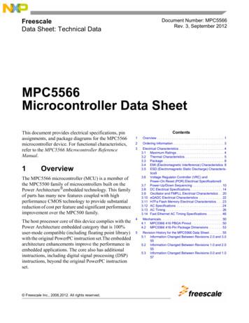
Ordering parts1 Ordering parts1.1 Determining valid orderable partsValid orderable part numbers are provided on the web.1. To determine the orderable part numbers for this device, go to www.nxp.com andsearch the required part number. The part numbering format is described in thesection that follows.2 Part identification2.1 DescriptionPart numbers for the chip have fields that identify the specific part. You can use thevalues of these fields to determine the specific part you have received.2.2 Part Number FormatThe figure below represents the format of part number of this device.VF6xx, VF5xx, VF3xx, Rev. 9, 01/2018NXP Semiconductors5
Part identificationM V F 5 0N S 15 1 C MK 40 RTape & ReelR Tape & Reel(Optional)Qualification StatusP engineering samplesM qualifiedSpeed (A5 core)26 266MHz40 400MHz50 500MHzBrand: V VybridSeries: F currentFamily3 Standard (A5 Only)5 Advanced (A5 Only)6 Dual Core (A5 & M4)PackageKU 176LQFPMK 364BGATemp SpecC -40 to 85C TaOption0N Standard1N L2 Cache2N M4 PrimaryRevision1 Rev.1.xSecurityN No SecurityS Security EnabledMemory Size15 1.5MBFigure 1. Part Number Format2.3 Part NumbersThis table lists the part numbers on the device.Part 2GNOLQFP-EP 176 24*24*1.6A5-266, No Security, 176LQFPMVF30NS152CKU263N02GNOLQFP-EP 176 24*24*1.6A5-266, Security, 176LQFPMVF50NN152CMK403N02GNOMAP 364 17*17*1.5 P0.8A5-400, No Security, 364BGAMVF50NN152CMK503N02GNOMAP 364 17*17*1.5 P0.8A5-400, Security, 364BGAMVF50NS152CMK403N02GNOMAP 364 17*17*1.5 P0.8A5-500, No Security, 364BGAMVF50NS152CMK503N02GNOMAP 364 17*17*1.5 P0.8A5-500, Security, 364BGAMVF51NN152CMK503N02GNOMAP 364 17*17*1.5 P0.8A5-500, L2 Cache, No Security,364BGAMVF51NS152CMK503N02GNOMAP 364 17*17*1.5 P0.8A5-500, L2 Cache, Security, 364BGAMVF60NN152CMK403N02GYESMAP 364 17*17*1.5 P0.8A5-400, M4, No Security, 364BGAMVF60NN152CMK503N02GYESMAP 364 17*17*1.5 P0.8A5-400, M4, Security, 364BGAMVF60NS152CMK403N02GYESMAP 364 17*17*1.5 P0.8A5-500, M4, No Security, 364BGATable continues on the next page.VF6xx, VF5xx, VF3xx, Rev. 9, 01/20186NXP Semiconductors
Terminology and guidelinesMVF60NS152CMK503N02GYESMAP 364 17*17*1.5 P0.8A5-500, M4, Security, 364BGAMVF61NN152CMK503N02GYESMAP 364 17*17*1.5 P0.8A5-500, M4, L2 Cache, No Security,MVF61NS152CMK503N02GYESMAP 364 17*17*1.5 P0.8A5-500, M4, L2 Cache, Security,MVF62NN152CMK403N02GYESMAP 364 17*17*1.5 P0.8A5-400, M4 Primary, No Security,364BGA3 Terminology and guidelines3.1 Definition: Operating requirementAn operating requirement is a specified value or range of values for a technicalcharacteristic that you must guarantee during operation to avoid incorrect operation andpossibly decreasing the useful life of the chip.3.1.1 ExampleThis is an example of an operating requirement:SymbolVDDDescription1.0 V core supplyvoltageMin.0.9Max.1.1UnitV3.2 Definition: Operating behaviorUnless otherwise specified, an operating behavior is a specified value or range of valuesfor a technical characteristic that are guaranteed during operation if you meet theoperating requirements and any other specified conditions.3.2.1 ExampleThis is an example of an operating behavior:SymbolIWPDescriptionDigital I/O weak pullup/ 10pulldown currentMin.Max.130UnitµAVF6xx, VF5xx, VF3xx, Rev. 9, 01/2018NXP Semiconductors7
Terminology and guidelines3.3 Definition: AttributeAn attribute is a specified value or range of values for a technical characteristic that areguaranteed, regardless of whether you meet the operating requirements.3.3.1 ExampleThis is an example of an attribute:SymbolCIN DDescriptionInput capacitance:digital pinsMin.—Max.7UnitpF3.4 Definition: RatingA rating is a minimum or maximum value of a technical characteristic that, if exceeded,may cause permanent chip failure: Operating ratings apply during operation of the chip. Handling ratings apply when the chip is not powered.3.4.1 ExampleThis is an example of an operating rating:SymbolVDDDescription1.0 V core supplyvoltageMin.–0.3Max.1.2UnitVVF6xx, VF5xx, VF3xx, Rev. 9, 01/20188NXP Semiconductors
Terminology and guidelines3.5 Result of exceeding a ratingFailures in time (ppm)4030The likelihood of permanent chip failure increases rapidly assoon as a characteristic begins to exceed one of its operating ratings.20100Operating ratingMeasured characteristic3.6 Relationship between ratings and operating pinratFatal rangeDegraded operating rangeNormal operating rangeDegraded operating rangeFatal rangeExpected permanent failure- No permanent failure- Possible decreased life- Possible incorrect operation- No permanent failure- Correct operation- No permanent failure- Possible decreased life- Possible incorrect operationExpected permanent failure– Operating (power on)ngdlinHaragtin)in.(mngdlinHaragtin.)ax(mFatal rangeHandling rangeFatal rangeExpected permanent failureNo permanent failureExpected permanent failure– Handling (power off) 3.7 Guidelines for ratings and operating requirementsFollow these guidelines for ratings and operating requirements: Never exceed any of the chip’s ratings. During normal operation, don’t exceed any of the chip’s operating requirements. If you must exceed an operating requirement at times other than during normaloperation (for example, during power sequencing), limit the duration as much aspossible.VF6xx, VF5xx, VF3xx, Rev. 9, 01/2018NXP Semiconductors9
Terminology and guidelines3.8 Definition: Typical valueA typical value is a specified value for a technical characteristic that: Lies within the range of values specified by the operating behavior Given the typical manufacturing process, is representative of that characteristicduring operation when you meet the typical-value conditions or other specifiedconditionsTypical values are provided as design guidelines and are neither tested nor guaranteed.3.8.1 Example 1This is an example of an operating behavior that includes a typical value:SymbolDescriptionIWPDigital I/O �A3.8.2 Example 2This is an example of a chart that shows typical values for various voltage andtemperature conditions:500045004000TJIDD STOP (μA)3500150 C3000105 C250025 C2000–40 C1500100050000.900.951.001.051.10VDD (V)VF6xx, VF5xx, VF3xx, Rev. 9, 01/2018
MVF60NS152CMK50 3N02G YES MAP 364 17*17*1.5 P0.8 A5-500, M4, Security, 364BGA MVF61NN152CMK50 3N02G YES