Transcription
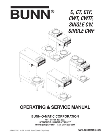
S i 3 2 2 60/1S INGLE - C HIP D UAL P RO S L I C Si32260/1 /CBAT b / SRINGCb542GPIO1b / STIPCbSRINGACaGPIO1a / REFSVBATa1136CAPPbSVDC1235CAPMbGND 414SDCHa13DCDRVaRSTBINTB / DTXENBVBATbRINGbTIPb4442VBATa4543RINGa46Si32260/1 6x8 mmGPIO2A / SRINGCa141VDDAGPIO1a / STIPCa240GPIO2b / SRINGCbSRINGDCa339GPIO1b / 3CAPPbSVDC1032CAPMbRSTB1131SVBATbINTB / 211820SDCLaGNDPADSDCHaThe Si32260/1 Dual ProSLIC devices, in a single package, implement two completeforeign exchange station (FXS) telephony interfaces. The Si32260/1 devices operate from a3.3 V supply and have standard PCM/SPI or GCI (8x8 mm package only) bus digitalinterfaces. A pair of built-in dc-dc converter controllers can be used to automaticallygenerate the optimal battery voltage required for each line-state, optimizing efficiency andminimizing heat generation. The Si32260/1 devices are designed to operate not only with atracking battery supply for each channel for lowest power consumption, but also with sharedbattery supplies, for lowest cost. When used with shared battery supplies, the internal dc-dccontroller operates in Tracking Shared Supply (TSS) mode to deliver power consumptionlower than typical fixed voltage shared rail designs (shared supplies are not currentlysupported by the 6 x 8 mm package option). Self-testing and metallic loop testing (MLT)(e.g., GR-909) is facilitated by the built-in DSP, monitor ADC, and test load. The devices areavailable with linefeed voltage ratings of –110 V (Si32260) or –140 V (Si32261) to supporthigh voltage ringing, and both devices support wideband audio for better-than-PSTN voicequality. The Si32260/1 devices are available in a 6 x 8 mm 47-pin QFN package or an8 x 8 mm 60-pin QFN package.453DCDRVaDescription219Wireless Fixed Terminals (WFT)Wireless Local Loop (WLL)WiMAX CPEPrivate Branch Exchange (PBX)VoIP MDU gateways1N/CDATAi TIPaGPIO2A / SRINGCaTIPaVoIP gateways and routersxDSL IADsOptical Network Terminals/Units (ONT/U)Analog Terminal Adapters (ATA)Cable eMTASi32260/1 8x8 mm47 Pin Assignments17ApplicationsSee page 45.16 Ordering Information18 17 Software-programmable parameters: Ringing frequency, amplitude,cadence, and waveshape Two-wire ac impedance Transhybrid balance DC current loop feed (10–45 mA) Loop closure and ring trip thresholds Ground key detect thresholdIntegrated dc-dc controllers with directconnection to MOSFETThree high voltage supply options Full tracking Tracking shared supplies Fixed railDTMF generator/decoderA-Law/µ-Law companding, linear PCMGCI/IOM-2 mode support3.3 V operationPb-free/RoHS-compliant packagingPCLK DATAo Two complete FXS channels in a single6 x 8 mm or 8 x 8 mm packagePerforms all BORSCHT functionsIdeal for short- or long-loop applicationsUltra low power consumptionInternal balanced or unbalanced ringingPatented low power ringingAdaptive ringingSimplified configuration and diagnostics Supported by ProSLIC API GR-909 loop diagnostics Audio diagnostics with loopback Integrated test loadWideband voice supportOn-hook transmissionLoop or ground start operationSmooth polarity reversalPulse meteringPCM and SPI bus digital interfaces withprogrammable interruptsSDITHRU Patents pendingRev. 1.4 4/14Copyright 2014 by Silicon LaboratoriesSi32260/1
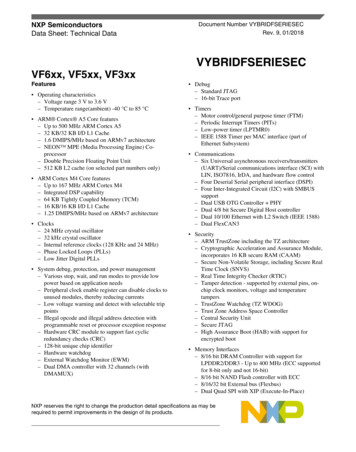
Si32260/1Caller IDCSSDISDOSCLKINTRSTPCLKDTMF &Tone CADCLinefeedControlDACLinefeedMonitorLine DiagnosticsPLLDC-DCDC-DC anceImpedanceand HybridFunctional Block DiagramTIPSi32260/12Confidential Rev. 1.4Channel ARINGChannel BRING
Si32260/1TABLE O F C ONTENTSSectionPage1. Electrical Specifications . . . . . . . . . . . . . . . . . . . . . . . . . . . . . . . . . . . . . . . . . . . . . . . . . . .52. Typical Application Circuits . . . . . . . . . . . . . . . . . . . . . . . . . . . . . . . . . . . . . . . . . . . . . . . 202.1. Flyback Tracking DC-DC Converter . . . . . . . . . . . . . . . . . . . . . . . . . . . . . . . . . . . . . 202.2. Low Cost Quasi Ćuk (LCQC) . . . . . . . . . . . . . . . . . . . . . . . . . . . . . . . . . . . . . . . . . . 233. Bill of Materials . . . . . . . . . . . . . . . . . . . . . . . . . . . . . . . . . . . . . . . . . . . . . . . . . . . . . . . . . . 264. Functional Description . . . . . . . . . . . . . . . . . . . . . . . . . . . . . . . . . . . . . . . . . . . . . . . . . . . 305. FXS Features . . . . . . . . . . . . . . . . . . . . . . . . . . . . . . . . . . . . . . . . . . . . . . . . . . . . . . . . . . .315.1. DC Feed Characteristics . . . . . . . . . . . . . . . . . . . . . . . . . . . . . . . . . . . . . . . . . . . . . . 315.2. Linefeed Operating States . . . . . . . . . . . . . . . . . . . . . . . . . . . . . . . . . . . . . . . . . . . . 315.3. Line Voltage and Current Monitoring . . . . . . . . . . . . . . . . . . . . . . . . . . . . . . . . . . . . 315.4. Power Monitoring and Power Fault Detection . . . . . . . . . . . . . . . . . . . . . . . . . . . . . . 315.5. Thermal Overload Shutdown . . . . . . . . . . . . . . . . . . . . . . . . . . . . . . . . . . . . . . . . . . 315.6. Loop Closure Detection . . . . . . . . . . . . . . . . . . . . . . . . . . . . . . . . . . . . . . . . . . . . . . . 335.7. Ground Key Detection . . . . . . . . . . . . . . . . . . . . . . . . . . . . . . . . . . . . . . . . . . . . . . . . 335.8. Ringing Generation . . . . . . . . . . . . . . . . . . . . . . . . . . . . . . . . . . . . . . . . . . . . . . . . . . 335.9. Polarity Reversal . . . . . . . . . . . . . . . . . . . . . . . . . . . . . . . . . . . . . . . . . . . . . . . . . . . . 355.10. Two-Wire Impedance Synthesis . . . . . . . . . . . . . . . . . . . . . . . . . . . . . . . . . . . . . . . 355.11. Transhybrid Balance Filter . . . . . . . . . . . . . . . . . . . . . . . . . . . . . . . . . . . . . . . . . . . 355.12. Tone Generators . . . . . . . . . . . . . . . . . . . . . . . . . . . . . . . . . . . . . . . . . . . . . . . . . . . 355.13. DTMF Detection . . . . . . . . . . . . . . . . . . . . . . . . . . . . . . . . . . . . . . . . . . . . . . . . . . . 355.14. Pulse Metering . . . . . . . . . . . . . . . . . . . . . . . . . . . . . . . . . . . . . . . . . . . . . . . . . . . .355.15. DC-DC Controller . . . . . . . . . . . . . . . . . . . . . . . . . . . . . . . . . . . . . . . . . . . . . . . . . . 355.16. Wideband Audio . . . . . . . . . . . . . . . . . . . . . . . . . . . . . . . . . . . . . . . . . . . . . . . . . . . 355.17. In-Circuit and Metallic Loop Testing (MLT) . . . . . . . . . . . . . . . . . . . . . . . . . . . . . . 366. System Interfaces . . . . . . . . . . . . . . . . . . . . . . . . . . . . . . . . . . . . . . . . . . . . . . . . . . . . . . . .376.1. SPI Control Interface . . . . . . . . . . . . . . . . . . . . . . . . . . . . . . . . . . . . . . . . . . . . . . . . .376.2. PCM Interface and Companding . . . . . . . . . . . . . . . . . . . . . . . . . . . . . . . . . . . . . . . . 377. Pin Descriptions: Si32260/1 . . . . . . . . . . . . . . . . . . . . . . . . . . . . . . . . . . . . . . . . . . . . . . . 387.1. Si32260/61 6x8 mm Package . . . . . . . . . . . . . . . . . . . . . . . . . . . . . . . . . . . . . . . . . .387.2. Si32260/61 8x8 mm Package . . . . . . . . . . . . . . . . . . . . . . . . . . . . . . . . . . . . . . . . . .418. Ordering Guide . . . . . . . . . . . . . . . . . . . . . . . . . . . . . . . . . . . . . . . . . . . . . . . . . . . . . . . . . . 459. Product Identification . . . . . . . . . . . . . . . . . . . . . . . . . . . . . . . . . . . . . . . . . . . . . . . . . . . .4710. Package Outlines . . . . . . . . . . . . . . . . . . . . . . . . . . . . . . . . . . . . . . . . . . . . . . . . . . . . . . . 4810.1. 47-Pin QFN/LGA (6x8 mm) . . . . . . . . . . . . . . . . . . . . . . . . . . . . . . . . . . . . . . . . . . . 4810.2. 60-Pin QFN/LGA (8x8 mm) . . . . . . . . . . . . . . . . . . . . . . . . . . . . . . . . . . . . . . . . . . . 4910.3. 60-Pin QFN (8x8 mm) . . . . . . . . . . . . . . . . . . . . . . . . . . . . . . . . . . . . . . . . . . . . . . . 5011. PCB Land Pattern—LGA Package . . . . . . . . . . . . . . . . . . . . . . . . . . . . . . . . . . . . . . . . . 5111.1. Land Pattern and Solder Mask Design–QFN-47 (6x8 mm) . . . . . . . . . . . . . . . . . . 5111.2. Land Pattern and Solder Mask Design–QFN-60 (8x8 mm) . . . . . . . . . . . . . . . . . . 5211.3. Thermal via Layout–QFN-47 (6x8 mm) . . . . . . . . . . . . . . . . . . . . . . . . . . . . . . . . . . 5311.4. Thermal via Layout–QFN-60 (8x8 mm) . . . . . . . . . . . . . . . . . . . . . . . . . . . . . . . . . . 53Confidential Rev. 1.43
Si32260/111.5. Stencil Aperture Design–QFN-47 (6x8 mm) . . . . . . . . . . . . . . . . . . . . . . . . . . . . . . 5411.6. Stencil Aperture Design–QFN-60 (8x8 mm) . . . . . . . . . . . . . . . . . . . . . . . . . . . . . . 5512. Top Markings . . . . . . . . . . . . . . . . . . . . . . . . . . . . . . . . . . . . . . . . . . . . . . . . . . . . . . . . . . 5612.1. Top Marking (47-Pin LGA) . . . . . . . . . . . . . . . . . . . . . . . . . . . . . . . . . . . . . . . . . . . 5612.2. Top Marking Explanation (47-pin LGA) . . . . . . . . . . . . . . . . . . . . . . . . . . . . . . . . . . 5612.3. Top Marking (60-Pin LGA) . . . . . . . . . . . . . . . . . . . . . . . . . . . . . . . . . . . . . . . . . . . 5712.4. Top Marking Explanation (60-Pin LGA) . . . . . . . . . . . . . . . . . . . . . . . . . . . . . . . . . 5713. Silicon Labs Si3226x Support Documentation . . . . . . . . . . . . . . . . . . . . . . . . . . . . . . .57Document Change List: . . . . . . . . . . . . . . . . . . . . . . . . . . . . . . . . . . . . . . . . . . . . . . . . . . . . .58Contact Information . . . . . . . . . . . . . . . . . . . . . . . . . . . . . . . . . . . . . . . . . . . . . . . . . . . . . . . .594Confidential Rev. 1.4
Si32260/11. Electrical SpecificationsTable 1. Recommended Operating Conditions1ParameterSymbolAmbient TemperatureTASilicon Junction Temperature,QFN-60, QFN-47Supply Voltage, Si32260/1MinTypMaxUnitF-grade02570 CG-grade–402585 CLinefeed Die——1452 CVDDD, �140—–15VBattery Voltage, Si32260Battery Voltage,TJHVTest ConditionNotes:1. All minimum and maximum specifications apply across the recommended operating conditions. Typical values apply atnominal supply voltages and an operating temperature of 25 C unless otherwise stated.2. Except during ringing.3. Operation at minimum voltage dependent upon loop conditions and dc-dc converter configuration.Table 2. AC CharacteristicsParameterTest ConditionMinTypMaxUnitTX/RX PerformanceOverload Compression2-Wire – PCMFigure 5——Single Frequency Distortion(0 dBm0 input)0 Hz to 4 kHz——–40dBm00 Hz – 12 kHz——–28dBm0200 Hz to 3.4 kHzD/A or A/D 8-bitActive off-hook, and OHT, any ZTFigure 4——0 dBm0, Active off-hook, andOHT, any Noise Distortion)Ratio1Audio Tone Generator Signal-toDistortion Ratio1Intermodulation DistortionGainAccuracy1Attenuation Distortion vs. Freq.2-Wire to PCM or PCM to 2-Wire1014 Hz, any gain setting0 dBm05Group Delay vs. FrequencySee Figure 6 and 7See Figure 8 and 9Notes:1. Analog signal measured as VTIP – VRING. Assumes ideal line impedance matching.2. The quantization errors inherent in the µ/A-law companding process can generate slightly worse gain trackingperformance in the signal range of 3 to –37 dB for signal frequencies that are integer divisors of the 8 kHz PCMsampling rate.3. VDDD, VDDA 3.3 V, VBAT –52 V, no fuse resistors; RL 600 , ZS 600 synthesized using RS registercoefficients.4. The level of any unwanted tones within the bandwidth of 0 to 4 kHz does not exceed –55 dBm.5. 0 dBm0 is equal to 0 dBm into 600 .Confidential Rev. 1.45
Si32260/1Table 2. AC Characteristics (Continued)Parameter2Gain TrackingMinTypMaxUnit3 dB to –37 dB——0.25dB–37 dB to –50 dB——0.5dB–50 dB to –60 dB——1.0dB1014 Hz, Within same time-slot—450500µs200 Hz to 3.4 kHz2630—dB300 Hz to 3.4 kHz2630—dBC-Message weighted—812dBrnCPsophometric weighted—–82–78dBmPRX and TX, 200 Hz to 3.4 kHz—55—dB200 Hz to 1 kHz5860—dB1 kHz to 3.4 kHz5358—dB200 Hz to 3.4 kHz40——dB200 Hz to 3.4 kHz at TIP or RING—50— Active off-hook 60 HzReg 73 0x0B—25—mA1014 Hz sine wave,reference level –10 dBmSignal level:Round-Trip Group Delay2-Wire Return LossTranshybridTest Condition3Balance3Noise PerformanceIdle Channel Noise4PSRR from VDDD, VDDA @ 3.3 VLongitudinal PerformanceLongitudinal to Metallic/PCMBalance (forward or reverse)Metallic/PCM to LongitudinalBalanceLongitudinal ImpedanceLongitudinal Current CapabilityNotes:1. Analog signal measured as VTIP – VRING. Assumes ideal line impedance matching.2. The quantization errors inherent in the µ/A-law companding process can generate slightly worse gain trackingperformance in the signal range of 3 to –37 dB for signal frequencies that are integer divisors of the 8 kHz PCMsampling rate.3. VDDD, VDDA 3.3 V, VBAT –52 V, no fuse resistors; RL 600 , ZS 600 synthesized using RS registercoefficients.4. The level of any unwanted tones within the bandwidth of 0 to 4 kHz does not exceed –55 dBm.5. 0 dBm0 is equal to 0 dBm into 600 .6Confidential Rev. 1.4
Si32260/1Table 3. Power Supply CharacteristicsParameterSupply currents:ResetSupply currents:High Impedance, OpenSupply currents:Forward/Reverse, On-hookSupply currents:Forward/Reverse, On-hookSupply currents:Tip/Ring Open, On-hookSupply currents:Tip/Ring Open, On-hookSymbolTest ConditionMinTypMaxUnitIDDVT and VR Hi-Z , RST 0—3.5—mA—0—mA—23—mA—0.6—mAVTR –48 V,Automatic Power Save Modeenabled—10—mA—0.4—mAVTR –48 V,Automatic Power Save Modedisabled—35—mA—2.2—mAVT or VR –48 VVR or VT Hi-Z,Automatic Power Save �mA—53—mA—3—mA—54—mA—2.2 TIDDIVBATIDDIVBATIDDIVBATSupply currents:Forward/Reverse OHT,On-hookSupply currents:Forward/Reverse Active,Off-hookSupply currents:RingingVT and VR Hi-ZIDDVT or VR –48 VVR or VT Hi-Z,Automatic Power Save ModeenabledVTR 48 VIVBATIDDILOOP 20 mA RLOAD 200 ΩIVBATIDDIVBATVTR 55VRMS 0 VDC,balanced, sinusoidal, f 20 Hz,RLOAD 5 REN 1400 Notes:1. All specifications are for a single channel of Si3226x with a tracking flyback dc-dc converter, when both channels arein the same operating state.2. ILOOP is the dc current in the subscriber loop during the off-hook state.Confidential Rev. 1.47
Si32260/1Table 4. Linefeed CharacteristicsParameterSymbolTest ConditionMinTypMaxUnitRLOOPRDC,MAX 430 ILOOP 18 mA, VBAT –52 V,RPROT 0 ——2000 Differential——45mACommon Mode——30mADifferential Common Mode——45mAILIM 18 mA——10%Active Mode; VOC 48 V,VTIP – VRING——4VRDOILOOP ILIM160—640 DC On-Hook VoltageAccuracy—Ground StartVOHTOIRING ILIM; VRING wrt ground,VRING –51 V——4VDC OutputResistance—Ground StartRROTOIRING ILIM; RING to ground160—640 DC Output Resistance—Ground StartRTOTOTIP to ground400——k Loop Closure DetectThreshold AccuracyITHR 13 mA——10%Ground Key DetectThreshold AccuracyITHR 13 mA——10%AC detection,VRING 70 Vpk, no offset,ITH 80mA——4mADC detection,20 V dc offset, ITH 13 mA——1mADC Detection,48 V DC offset, Rloop 1500 ——3mASi32260 Open circuit,VBAT –110 V—–108—VPKSi32261 Open circuit,VBAT –140 V—–136—VPK—1—%f 16 Hz to 60 Hz——1%Accuracy of ON/OFF times——50msMaximum Loop ResistanceDC Feed CurrentDC Loop Current AccuracyDC Open Circuit VoltageAccuracyDC Differential OutputResistanceRing TripThreshold AccuracyRinging Amplitude*Sinusoidal Ringing TotalHarmonic DistortionRinging Frequency AccuracyRinging Cadence AccuracyVRINGINGRTHDSi32260 : 60 VRMS,15 VOFFSET, 0–5 RENSi32261 : 55 VRMS,48 VOFFSET, 0–5 REN*Note: Ringing amplitude is set for 108 or 128 V peak and measured at TIP-RING using no series protection resistance.8Confidential Rev. 1.4
Si32260/1Table 4. Linefeed Characteristics (Continued)ParameterSymbolTest ConditionMinTypMaxUnitVTIP – VRING 48 V—24%ILOOP 18 mA—710%Power Threshold 1.0 WVBAT –56 V, ILDDD 40 mA,RLOAD 600 —15—%RTESTHVIC STATE SPARE[23] 1; VT/R 50 V1.0—3.0k VTLHVIC STATE SPARE[23] 1 5 50VLoop Voltage SenseAccuracyLoop CurrentSense AccuracyPower AlarmThreshold AccuracyTest Load ImpedanceTest Load Voltage*Note: Ringing amplitude is set for 108 or 128 V peak and measured at TIP-RING using no series protection resistance.Table 5. Digital I/O CharacteristicsParameterSymbolHigh Level Input VoltageMinTypMaxUnitVIH2.0—VDDVLow Level Input VoltageVIL0—0.8VHigh Level OutputVoltageVOHDTX, SDO, SDITHRU,GPIO1/STIPC, GPIO2/SRINGC:IO –4 mAVDD – 0.6——VVOLDTX, SDO, INT,SDITHRU,GPIO1/STIPC, GPIO2/SRINGC:IO 4 mA——0.4V334280µA——10µALow Level OutputVoltageTest ConditionSDITHRU and RSTInternal Pullup CurrentInput Leakage CurrentILConfidential Rev. 1.49
Si32260/1Table 6. Charge Pump CharacteristicsParameterSymbolTest ConditionMinTypMaxUnitOutput Voltage(DCDRVa/b, DCFFa/b)VCP2 x VDD – 1—2xVDDVOutput CurrentICP——3*mA*Note: Peak drive current capability is 60 mA.Table 7. Switching Characteristics—General �µsRST Pulse Width*Note: All timing is referenced to the 50% level of the waveform. Input test levels areVIH VDD – 0.4 V, VIL 0.4 V. Rise and Fall times are referenced to the 20% and 80% levels of the waveform.PCLKCounting of PCLKRising Edges3130292854321012345282930RSTBNote: The count of PCLK rising edges during reset will be skewed by 1-2 clocks based on the internal sampling of reset.Figure 1. Reset Timing Diagram10Confidential Rev. 1.431
Si32260/1Table 8. Switching Characteristics—SPIParameterSymbolTest ConditionMinTypMaxUnitCycle Time SCLKtc62——nsRise Time, SCLKtr——25nsFall Time, SCLKtf——25nsDelay Time, SCLK Fall to SDO Activetd1——20nsDelay Time, SCLK Fall to SDOTransitiontd2——20nsDelay Time, CSB Rise to SDO Tristatetd3——20nsSetup Time, CSB to SCLK Falltsu125——nsHold Time, CSB to SCLK Riseth120——nsSetup Time, SDI to SCLK Risetsu225——nsHold Time, SDI to SCLK Riseth220——nsDelay Time between Chip Selectstcs220——nsSDI to SDITHRU Propagation Delaytd4—410nsNotes:1. All timing is referenced to the 50% level of the waveform. Input test levels are VIH VDDD –0.4 V, VIL 0.4 V.2. Characteristics for outputs specified with CL 20 4SDITHRUFigure 2. SPI Timing DiagramConfidential Rev. 1.411
Si32260/1Table 9. Switching Characteristics—PCM Highway Interface1ParameterPCLK PeriodSymbolTestConditiontpPCLK Jitter Valid PCLK MHzMHzMHzMHzMHzFSYNC Period4tfs—125—µsPCLK Duty Cycle Tolerancetdty405060%tjitter—— 120nsRise Time, PCLKtr——25nsFall Time, PCLKtf——25nsDelay Time, PCLK Rise to DTX Activetd1——20nsDelay Time, PCLK Rise to DTXTransitiontd2——20nsDelay Time, PCLK Rise to DTX Tristate6td3——20nsSetup Time, FSYNC to PCLK Falltsu125——nsHold Time, FSYNC to PCLK Fallth120——nsSetup Time, DRX to PCLK Falltsu225——nsHold Time, DRX to PCLK Fallth220——nsFSYNC Pulse Widthtwfstp—125 µs–tpFSYNC JitterTolerance5Notes:1. Characteristics for outputs specified with CL 20 pF.2. All timing is referenced to the 50% level of the waveform. Input test levels are VIH – VI/O – 0.4 V, VIL 0.4 V.3. A constant PCLK and FSYNC are required.4. FSYNC source is assumed to be 8 kHz under all operati
3.3 V supply and have standard PCM/SPI or GCI (8x8 mm package only) bus digital interfaces. A pair of built-in dc-dc converter controllers can be used to automatically generate the optimal battery voltage required for each line-state, optimizing efficiency and minimizing heat generation. The