Transcription
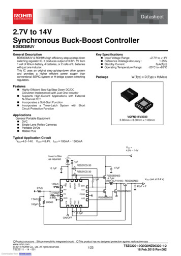
Datasheet2.7V to 14VSynchronous Buck-Boost ControllerBD8303MUVGeneral DescriptionKey SpecificationsBD8303MUV is ROHM’s high efficiency step-up/step-downswitching regulator IC. It produces output of 3.3V / 5V from1 cell of lithium battery, 4 batteries, or 2 cells of Li batterieswith just one inductor.This IC uses an original step-up/step-down drive systemand provides a higher efficient power supply thanconventional SEPIC-system or H-bridge system switchingregulators. Input Voltage Range:Reference Volatage Accuracy :Standby Current:Operating Temperature Range:Package 2.7V to 14V1.25%0μA(Typ)-25 C to 85 CW(Typ) x D(Typ) x H(Max)Features Highly-Efficient Step-Up/Step-Down DC/DCConverter Implemented with Just One InductorSupports High-Current Applications with ExternalN-Channel FETIncorporates a Soft-Start FunctionIncorporates a Timer-Latch System with ShortCircuit Protection FunctionApplicationsVQFN016V30303.00mm x 3.00mm x 1.00mmGeneral Portable Equipment DVC Single-Lens Reflex Cameras Portable DVDs Mobile PCsTypical Application CircuitVCC 4.0 14V,VOUT 8.4V, IOUT 100mA 1500mAVCC 4.0V – 14VInsert a filteras K SLF10165) RSS065N03VOUT (set at 8.4 V)47μF x kΩRTVREG100kΩ27kΩVCC0.1μF0.1μFON/OFF Product structure:Silicon monolithic integrated circuitwww.rohm.com 2014 ROHM Co., Ltd. All rights reserved.TSZ22111・14・001Downloaded from Arrow.com. This product has no designed protection against radioactive rays1/23TSZ02201-0Q3Q0NZ00320-1-216.Feb.2015 Rev.002
BD8303MUVPin ConfigurationPin DescriptionsPin No.RTINVFBRTOscillation frequency set terminalINVError AMP input terminal3FBError AMP output terminal4GNDGround terminal5STBON/OFF terminalSW16BOOT2LG17HG2Output side high-side FET gate drive terminalPGND8SW2Output side coil connecting terminal9LG2Output side low-side FET gate drive terminal10PGND11LG1Input side low-side FET gate drive terminal12SW1Input side coil connecting terminal13HG1Input side high-side FET gate drive terminal14BOOT115REG5V Internal regulator output terminal16VCCPower input terminalSW2HG2BOOT2STBFunction2LG2GNDPin Name1HG1BOOT1REGVCCTOP VIEWOutput side high-side driver input terminalDriver part ground terminalInput side high-side driver input terminalREGBlock DiagramREGTIMINGCONTROLTIMINGCONTROLwww.rohm.com 2014 ROHM Co., Ltd. All rights reserved.TSZ22111・15・001Downloaded from Arrow.com.2/23TSZ02201-0Q3Q0NZ00320-1-216.Feb.2015 Rev.002
BD8303MUVDescription of Blocks1. VREFThis block generates ERROR AMP reference voltage. The reference voltage is set to 1.0V.2. VREGThis is a voltage regulator block which outputs 5.0V and is used as power supply for IC internal circuit and BOOT pinsupply. Follows power supply voltage when 5.0V or below while the output voltage drops at the same time.An external 1.0µF capacitor is recommended to prevent oscillation.3. UVLOThis block prevents the malfunction of the internal circuitry during start-up or when the supply drops below a certainvoltage. When VREG is below 2.4V, the HG1, HG2, LG1 and LG2 pin is low, this block turns OFF all FET and DC/DCconverter outputs and resets the timer latch of the internal SCP circuit and soft-start circuit4. SCPThis block is the Short Circuit Protection that uses a Timer Latch System. It has an internal counter that is in synch withOSC. When the INV pin is set to 1.0V or lower voltage, the internal counter will count about 8200 pulses after which thelatch circuit will activate Turning OFF the DC/DC converter output (13.6msec when RRT 51kΩ). Restarting the STB pinor the supply voltage will reset the latch circuit.5. OSCThe OSC block generates the internal frequency of the IC. The frequency can be varied depending on the value of theexternal resistance of the RT pin (Pin 1).When RRT 51kΩ, the operation frequency is set to 600kHz.6. ERROR AMPThe ERROR AMP block detects output signals and PWM control signals and compares them with an internal referencevoltage set at 1.0V.7.PWM COMPThe PWM COMP block is a Voltage-to-Pulse Width converter that controls the output voltage depending on the inputvoltage. This block controls the pulse width by comparing the internal SLOPE waveform with the ERROR AMP outputvoltage. The output signal of the PWM COMP block is then fed to the driver. Max Duty and Min Duty are set at theprimary side and the secondary side of the inductor respectively, which are as follows:Primary side (SW1)Secondary side (SW2)HG1 Max DutyHG1 Min DutyLG2 Max DutyLG2 Min Duty::::About 90%,0%About 90%,About 10%,8. SOFT STARTThis block prevents in-rush current during start-up by bringing the output voltage of the DCDC converter into a soft-start.The Soft-Start block is in synch with the internal OSC block. This block enables the output voltage of the DCDCconverter to reach the set voltage after about 2400 pulses (4msec when RRT 51kΩ).9. N-Channel DRIVERThis block consists of a CMOS inverter circuit that drives the built-in N-Channel FET. It provides dead time for preventingfeed through during switching of HG1 L to LG1 H to HG2 L to LG2 H and LG1 L to HG1 H, LG2 L to HG2 H. The dead time is set at about 100nsec for each individual SWs10. ON/OFF LOGICThis block enables and disables the IC depending on the voltage applied at STB pin (Pin 5). The IC Turns ON when STBvoltage is 2.5 V or higher and it Turns OFF when STB is open or when 0V is applied. The STB pin has a pull-downresistor of approximately 400kΩ.www.rohm.com 2014 ROHM Co., Ltd. All rights reserved.TSZ22111・15・001Downloaded from Arrow.com.3/23TSZ02201-0Q3Q0NZ00320-1-216.Feb.2015 Rev.002
BD8303MUVAbsolute Maximum RatingsParameterMaximum Applied Power VoltagePower DissipationOperating Temperature RangeStorage Temperature RangeJunction TemperatureSymbolVCCVREGBetweenVBOOT1 , VBOOT2and VSW1, VSW2BetweenVBOOT1 , VBOOT2and GNDVSW1 and VSW2PdRating157UnitVV7V20V15(Note 1)0.62VWTopr-25 to 85 CTstg-55 to 150 CTjmax 150 C(Note 1) When installed on a 70.0 mm x 70.0 mm x 1.6 mm glass epoxy board. The rating is reduced by 4.96 mW/ C at Ta 25 C or more.Caution: Operating the IC over the absolute maximum ratings may damage the IC. The damage can either be a short circuit between pins or an open circuitbetween pins and the internal circuitry. Therefore, it is important to consider circuit protection measures, such as adding a fuse, in case the IC is operated over theabsolute maximum ratings.Recommended Operating ConditionsParameterSymbolStandard ValueMinTypMax-14UnitPower Supply Voltage RangeVCC2.7Output Voltage RangeVOUT1.8-12VOscillation Frequency RangefOSC0.20.61.0MHzwww.rohm.com 2014 ROHM Co., Ltd. All rights reserved.TSZ22111・15・001Downloaded from 5 Rev.002
BD8303MUVElectrical Characteristics (Unless otherwise specified, Ta 25 C, VCC 7.4V)ParameterSymbolTarget V Threshold VoltageVINV0.98751.001.0125VInput Bias CurrentIINV-500 50nASoft-Start TimetSS2.44.05.6msecOutput Source CurrentIEO102030μAVINV 0.8V , VFB 1.5VOutput Sink CurrentIEI0.61.33mAVINV 1.2V , VFB 1.5VSW1 Max DutyDMAX1859095%HG1 ONSW2 Max DutyDMAX2859095%LG2 ONSW2 Min DutyDMIN251015%LG2 OFFHG1, 2 High side ON-ResistanceRONHP-48ΩHG1, 2 Low side ON-ResistanceRONHN-48ΩLG1, 2 High side ON-ResistanceRONLP-48ΩLG1, 2 Low side ON-ResistanceRONLN-48ΩHG1-LG1 Dead TimetDEAD150100200nsecHG2-LG2 Dead TimetDEAD250100200nsecUVLODetection Threshold VoltageHysteresis RangeVREG monitorOscillatorOscillation FrequencyRRT 51kΩRegulatorOutput VoltageError AMPVCC 12.0V, VINV 6.0VRRT 51kΩPWM ionVSTBL-0.3- 0.3VRSTB250400700kΩISTB--1μAVCC Circuit CurrentICC1-6501000μAVINV 1.2VBOOT1 and BOOT2 Circuit CurrentICC2-120240μAVINV 1.2VSTB pinControl VoltageSTB Pin Pull-Down ResistanceCircuit CurrentStandby CurrentVCC Pinwww.rohm.com 2014 ROHM Co., Ltd. All rights reserved.TSZ22111・15・001Downloaded from Arrow.com.5/23TSZ02201-0Q3Q0NZ00320-1-216.Feb.2015 Rev.002
BD8303MUV1.0501.0501.0251.025VREF Voltage [V]VREF Voltage [V]Typical Performance Curves(Unless otherwise specified, Ta 25 C, VCC 0Ambient Temperature [ C]VCC Voltage [V]Figure 2. VREF Voltage vs Ambient TemperatureFigure 1. VREF Voltage vs VCC Voltage6.05.3005.05.200REG Voltage : VREG [V]REG Voltage : VREG -40VCC Voltage [V]Downloaded from Arrow.com.4080120Ambient Temperature [ C]Figure 3. REG Voltage vs VCC Voltagewww.rohm.com 2014 ROHM Co., Ltd. All rights reserved.TSZ22111・15・0010Figure 4. REG Voltage vs Ambient 5 Rev.002
BD8303MUVTypical Performance Curves - continued800700660700Oscillation Frequency [kHz]Oscillation Frequency VCC Voltage [V]04080120Ambient Temperature [ C]Figure 5. Oscillation Frequency vs VCC VoltageFigure 6. Oscillation Frequencyvs Ambient Temperature900800800750600VCC Current [μA]VCC Current C Voltage [V]Downloaded from Arrow.com.4080120Ambient Temperature [ C]Figure 7. VCC Current vs VCC Voltagewww.rohm.com 2014 ROHM Co., Ltd. All rights reserved.TSZ22111・15・0010Figure 8. VCC Current vs Ambient 5 Rev.002
BD8303MUVTypical Performance Curves - continued5.0501405.025100OUT Voltage : VOUT [V]BOOT Pin Current [μA]1208060405.0004.975204.95000123450651015BOOT Pin Voltage [V]VCC Voltage [V]Figure 9. BOOT Pin Current vs BOOT Pin VoltageFigure 10. OUT Voltage vs VCC Voltage(Line Regulation)1005.050SW1 Max Duty90SW2 Max Duty7060Duty [%]OUT Voltage : VOUT [V]805.0255.0005040304.97520SW2 Min Duty1004.95005001000-401500Load Current [mA]Downloaded from Arrow.com.4080120Ambient Temperature [ ]Figure 11. OUT Voltage vs Load Current(Load Regulation)www.rohm.com 2014 ROHM Co., Ltd. All rights reserved.TSZ22111・15・0010Figure 12.MAX Duty / MIN Duty vs Ambient 5 Rev.002
BD8303MUVTypical Performance Curves - continued100100VCC 7.4VVCC 5.0V9090VCC 3.7V8080VCC 3.0VVCC 4.0VVCC 4.2V70Efficiency [%]Efficiency [%]70605040VCC 14V6050403030202010100001000200003000Load Current [mA]50010001500Load Current [mA]Figure 13. Efficiency vs Load Current(Example of Application Circuit [1](VOUT 3.3V))Figure 14. Efficiency vs Load Current(Example of Application Circuit [2](VOUT 5.0V))10090VCC 7.4V80VCC 4.0VVCC 10VEfficiency [%]7060504030201000500100015002000Load Current [mA]Figure 15. Efficiency vs Load Current(Example of Application Circuit [3](VOUT 8.4V)www.rohm.com 2014 ROHM Co., Ltd. All rights reserved.TSZ22111・15・001Downloaded from Arrow.com.9/23TSZ02201-0Q3Q0NZ00320-1-216.Feb.2015 Rev.002
BD8303MUVTypical WaveformsVOUT (2.0V/div)200μsec/div500nsec/divFigure 16. Starting WaveformExample of Application Circuit [2](L 10µH, COUT 47µH, fOSC 750 kHz, unloaded)Figure 17. Oscillation Waveform(VCC 5.0V, VOUT 5.0V, ILOAD 1000mA)VOUT (100mV/div)ILOAD(500mA/div)500μsec/divFigure 18. Load Variation WaveformExample of Application Circuit [2](VCC 7.4V, VOUT 5.0V,ILOAD 200mA 1000mA :40 mA/µsec)www.rohm.com 2014 ROHM Co., Ltd. All rights reserved.TSZ22111・15・001Downloaded from 5 Rev.002
BD8303MUVApplication InformationPower Dissipation [mW]1. Package Heat Reduction CurveAmbient Temperature [ C]Figure 19. Power Dissipation vs Ambient TemperatureHeat Reduction Curve (IC alone)when used at Ta 25 C or more, it is reduced by 4.96 mW/ C.2. Example of Application Circuit(1) Application Circuit [1]: Input: 2.7V to 5.5V, Output: 3.3V / 100mA to 2000mAVCC 2.7 V – 5.5 VInsert a filter .2kΩVOUT (set at 3.3 V)(TDK SLF10165) gure 20. Example of Application Circuit [1]www.rohm.com 2014 ROHM Co., Ltd. All rights reserved.TSZ22111・15・001Downloaded from 5 Rev.002
BD8303MUV(2) Application Circuit [2]: Input: 2.7V to 14 V, Output : 5.0V / 100 mA to 1500 mAVCC 2.7 V –14 VInsert a filteras N034.7μHINV4700pFSW1VOUT (set at 5.0 045N03PGNDGND120kΩ(TDK VCC0.1μF0.1μFON/OFFFigure 21. Example of Application Circuit [2](3) Application Circuit [3]: Input : 4.0V to 14V, Output : 8.4V / 100mA to 1500mAVCC 4.0V – 14VInsert a filteras K SLF10165) RSS065N03VOUT (set at 8.4 V)47μF x kΩRTVREG100kΩ27kΩVCC0.1μF0.1μFON/OFFFigure 22. Example of Application Circuit [3]www.rohm.com 2014 ROHM Co., Ltd. All rights reserved.TSZ22111・15・001Downloaded from 5 Rev.002
BD8303MUV(4) Application Circuit [4]: Input : 2.7V to 14V, Output : 12V / 100mA to 1500mAVCC 4.0 V – 14 VInsert a filteras N0310μHHG1BOOT1(TDK SLF10165) RSS065N03VOUT(set at 12 0kΩVCC0.1μF0.1μFON/OFFFigure 23. Example of Application Circuit (4)3.Selection of Parts for Applications(1) Output InductorA shielded inductor that satisfies the current rating (current value, I PEAK as shown in Figure 24 Ripple Current) andhas a low DCR (direct current resistance component) is recommended. Inductor values greatly affect the output ripplecurrent. Ripple current can be reduced as th
voltage. When VREG is below 2.4V, the HG1, HG2, LG1 and LG2 pin is low, this block turns OFF all FET and DC/DC converter outputs and resets the timer latch of the internal SCP circuit and soft-start circuit 4. SCP This block is the Short Circuit Protection that uses a Timer Latch System. It has an internal counter that is in synch with OSC. When the INV pin is set to 1.0V or lower voltage, the internal counter will