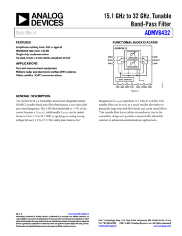
Transcription
Wideband 4 GHz, 43 dB Isolation at 1 GHz,CMOS 1.65 V to 2.75 V, 2:1 Mux/SPDTADG918/ADG919Data SheetFEATURESFUNCTIONAL BLOCK DIAGRAMSWideband switch: 3 dB at 4 GHzAbsorptive/reflective switchesHigh off isolation (43 dB at 1 GHz)Low insertion loss (0.8 dB at 1 GHz)Single 1.65 V to 2.75 V power supplyCMOS/LVTTL control logic8-lead MSOP and tiny 3 mm 3 mm LFCSPLow power consumption ( 1 9Wireless communicationsGeneral-purpose RF switchingDual-band applicationsHigh speed filter selectionDigital transceiver front end switchIF switchingTuner modulesAntenna diversity switchingRF1RFCRF203335-001CTRLFigure 2.GENERAL DESCRIPTIONPRODUCT HIGHLIGHTSThe ADG918/ADG919 are wideband switches using a CMOSprocess to provide high isolation and low insertion loss to1 GHz. The ADG918 is an absorptive (matched) switch having50 Ω terminated shunt legs, whereas the ADG919 is a reflectiveswitch. These devices are designed such that the isolation ishigh over the dc to 1 GHz frequency range. They have on-boardCMOS control logic, thus eliminating the need for externalcontrolling circuitry. The control inputs are both CMOS andLVTTL compatible. The low power consumption of theseCMOS devices makes them ideally suited to wireless andgeneral-purpose high frequency switching 0–3.0–40–3.210k–50VDD 2.5VTA 25 C100k1M10M100MFREQUENCY (Hz)1G10G03335-004ISOLATION (dB)VDD 2.5VTA 25 C–0.4INSERTION LOSS (dB)0–10 43 dB off isolation at 1 GHz.0.8 dB insertion loss at 1 GHz.Tiny 8-lead MSOP/LFCSP.Figure 3. Insertion Loss vs. REQUENCY (Hz)1G10G03335-003S21–90Figure 1. Off Isolation vs. FrequencyRev. EDocument FeedbackInformation furnished by Analog Devices is believed to be accurate and reliable. However, noresponsibility is assumed by Analog Devices for its use, nor for any infringements of patents or otherrights of third parties that may result from its use. Specifications subject to change without notice. Nolicense is granted by implication or otherwise under any patent or patent rights of Analog Devices.Trademarks and registered trademarks are the property of their respective owners.One Technology Way, P.O. Box 9106, Norwood, MA 02062-9106, U.S.A.Tel: 781.329.4700 2003–2016 Analog Devices, Inc. All rights reserved.Technical Supportwww.analog.com
ADG918/ADG919Data SheetTABLE OF CONTENTSFeatures . 1Terminology . 10Applications . 1Test Circuits . 11Functional Block Diagrams . 1Applications Information . 13General Description . 1Absorptive vs. Reflective Switch . 13Product Highlights . 1Wireless Metering. 13Revision History . 2Tuner Modules . 13Specifications. 3Filter Selection . 13Absolute Maximum Ratings. 5ADG918/ADG919 Evaluation Board . 14ESD Caution . 5Outline Dimensions . 15Pin Configuration and Function Descriptions . 6Ordering Guide . 16Typical Performance Characteristics . 7REVISION HISTORY5/2016—Rev. D to Rev. EUpdated Outline Dimensions . 153/2016—Rev. C to Rev. DChanged CP-8-2 to CP-8-13 . ThroughoutChanges to Figure 4 and Table 3 . 6Added Figure 5, Renumbered Sequentially . 6Changed ADG9xx Evaluation Board Section to ADG918/ADG919 Evaluation Board Section . 14Updated Outline Dimensions . 15Changes to Ordering Guide . 169/08—Rev. B to Rev. CChanges to Ordering Guide . 168/2008—Rev. A to Rev. BChanges to Table 1, AC Electrical Characteristics, Third OrderIntermodulation Intercept .3Updated Outline Dimensions . 15Changes to Ordering Guide . 169/2004—Rev. 0 to Rev. AUpdated Format . UniversalChange to Data Sheet Title .1Change to Features .1Change to Product Highlights .1Changes to Specifications .3Change to ADG9xx Evaluation Board section . 13Changes to Ordering Guide . 148/03—Revision 0: Initial VersionRev. E Page 2 of 16
Data SheetADG918/ADG919SPECIFICATIONSVDD 1.65 V to 2.75 V, GND 0 V, input power 0 dBm, all specifications TMIN to TMAX, unless otherwise noted. Temperature range forB Version: 40 C to 85 C.Table 1.ParameterAC ELECTRICAL CHARACTERISTICSOperating Frequency 23 dB Frequency 3Input Power3SymboltONtOFFtRISEtFALLP–1 dBIP30 V dc bias0.5 V dc biasDC to 100 MHz; VDD 2.5 V 10%500 MHz; VDD 2.5 V 10%1000 MHz; VDD 2.5 V 10%100 MHz500 MHz1000 MHz100 MHz500 MHz1000 MHz100 MHz500 MHz1000 MHz100 MHz500 MHz1000 MHzDC to 100 MHz500 MHz1000 MHzDC to 100 MHz500 MHz1000 MHz50% CTRL to 90% RF50% CTRL to 10% RF10% to 90% RF90% to 10% RF1000 MHz900 MHz/901 MHz, 4 dBmVINHVINHVINLVINLIIVDD 2.25 V to 2.75 VVDD 1.65 V to 1.95 VVDD 2.25 V to 2.75 VVDD 1.65 V to 1.95 V0 V VIN 2.75 VS21, S12Isolation—RFC to RF1/RF2(CP Package)S21, S12Isolation—RFC to RF1/RF2(RM Package)S21, S12Isolation—RF1 to RF2 (Crosstalk)(CP Package)S21, S12Isolation—RF1 to RF2 (Crosstalk)(RM Package)S21, S12Return Loss (On Channel)3S11, S22Return Loss (Off Channel)3ADG918S11, S22Input Low VoltageInput Leakage CurrentMinB VersionTyp 1dcInsertion LossOn Switching Time3Off Switching Time3Rise Time3Fall Time31 dB Compression3Third Order Intermodulation InterceptVideo Feedthrough 4DC ELECTRICAL CHARACTERISTICSInput High VoltageTest Conditions/CommentsRev. E Page 3 of dBdBdBdB109.5991.70.65 VCC 0.10.70.35 VCC 1dBdBdBdBdBdBnsnsnsnsdBmdBmmV p-pVVVVµA
ADG918/ADG919ParameterCAPACITANCE3RF On CapacitanceCTRL Input CapacitancePOWER REQUIREMENTSVDDQuiescent Power Supply CurrentData SheetSymbolTest Conditions/CommentsCRF ONCCTRLf 1 MHzf 1 MHzIDDDigital inputs 0 V or VDDMinB VersionTyp 1Max1.621.650.1UnitpFpF2.751VµATypical values are at VDD 2.5 V and 25 C, unless otherwise stated.Point at which insertion loss degrades by 1 dB.3Guaranteed by design, not subject to production test.4The dc transience at the output of any port of the switch when the control voltage is switched from high to low or low to high in a 50 Ω test setup, measured with 1 nsrise time pulses and 500 MHz bandwidth.12Rev. E Page 4 of 16
Data SheetADG918/ADG919ABSOLUTE MAXIMUM RATINGSTA 25 C, unless otherwise noted.Table 2.ParameterVDD to GNDInputs to GNDContinuous CurrentInput PowerOperating Temperature RangeIndustrial (B Version)Storage Temperature RangeJunction TemperatureθJA Thermal ImpedanceMSOPLFCSP2-Layer Board4-Layer BoardLead Temperature, Soldering (10 sec)IR Reflow, Peak Temperature ( 20 sec)ESDRating 0.5 V to 4 V 0.5 V to VDD 0.3 V130 mA18 dBmStresses at or above those listed under Absolute MaximumRatings may cause permanent damage to the product. This is astress rating only; functional operation of the product at theseor any other conditions above those indicated in the operationalsection of this specification is not implied. Operation beyondthe maximum operating conditions for extended periods mayaffect product reliability.ESD CAUTION 40 C to 85 C 65 C to 150 C150 C206 C/W84 C/W48 C/W300 C235 C1 kVRF1 and RF2 off port inputs to ground: 0.5 V to VDD – 0.5 V.1Rev. E Page 5 of 16
ADG918/ADG919Data SheetPIN CONFIGURATIONS AND FUNCTION DESCRIPTIONSRFC 4TOP VIEW(Not to Scale)8RF17GND6GND5RF2VDD 18 RF1CTRL 2ADG918/ADG9197 GNDGND 3TOP VIEW(Not to Scale)6 GNDRFC 45 RF2NOTES1. EXPOSED PAD. TIE THE EXPOSEDPAD TO SUBSTRATE, GND.03335-030GND 3ADG918/ADG91903335-002VDD 1CTRL 2Figure 5. ADG918/ADG919 Pin Configuration (LFCSP)Figure 4. ADG918/ADG919 Pin Configuration (MSOP)Table 3. Pin Function DescriptionsPin No.MSOP123, 6, 7458Not applicableLFCSP123, 6, 74580MnemonicVDDCTRLGNDRFCRF2RF1EPADFunctionPower Supply Input. These devices can be operated from 1.65 V to 2.75 V; decouple VDD to GND.Logic Control Input. See Table 4.Ground Reference Point for All Circuitry on the Device.COMMON RF Port for Switch.RF2 Port.RF1 Port.Exposed Pad. Tie the exposed pad to substrate, GND.Table 4. Truth TableCTRL01Signal PathRF2 to RFCRF1 to RFCRev. E Page 6 of 16
Data SheetADG918/ADG919TYPICAL PERFORMANCE 6VDD 2.5V–0.8 25 CVDD 2.75VINSERTION LOSS –2.8TA 25 C100k1M10M100MFREQUENCY (Hz)1G10G03335-017–3.210k–3.210kFigure 6. Insertion Loss vs. Frequency over Supplies(RF1/RF2, S12, and S21)–10–0.4010M100MFREQUENCY (Hz)1G10GVDD 1.65V TO 2.75VTA 25 C–20–0.45ISOLATION (dB)INSERTION LOSS (dB)1M0VDD 2.75V–0.35VDD 2.5V–0.50VDD ��70–0.70–0.75–80TA 25 C100k1M10M100MFREQUENCY (Hz)1G10G–9010k03335-019–0.8010kFigure 7. Insertion Loss vs. Frequency over Supplies (RF1/RF2,S12, and S21) (Zoomed Figure 5 Plot)S21100k1M10M100M1G10GFREQUENCY (Hz)Figure 10. Isolation vs. Frequency over Supplies (RF1/RF2, ADG918)0–0.2–0.4–10–0.6VDD 1.8VVDD 1.65VVDD 1.95VVDD 1.65V TO 2.75VTA 25 C–20–1.0–30–1.2ISOLATION 0TA 25 C1M10M100MFREQUENCY (Hz)1G10G–10010k100k1M10M100M1G10GFREQUENCY (Hz)Figure 11. Isolation vs. Frequency over Supplies (RF1/RF2, ADG919)Figure 8. Insertion Loss vs. Frequency over Supplies(RF1/RF2, S12, and S21)Rev. E Page 7 of 1603335-022–2.603335-021INSERTION LOSS (dB)100kFigure 9. Insertion Loss vs. Frequency over Temperature(RF1/RF2, S12, and S21)–0.30–0.8VDD 2.5V–3.003335-020INSERTION LOSS (dB)–1.2–3.0 85 C–1.003335-018–0.8 V 2.25VDD–1.0–40 C
ADG918/ADG919Data Sheet–10VDD 2.5V–20CH1–30S12 ( 85 C)–50–60CH2/3S12 ( 25 C)–70S12 (–40 C)–80–9010k100k1M10M100M1G10GFREQUENCY (Hz)CH1 CTRL 1V/DIVTRISE 6.1nsCH2 RF1 100mV/DIVTFALL 6.1ns03335-024S21(–40 C, 25 C, 85 C)–10003335-023ISOLATION (dB)–40CH3 RF2 100mV/DIVFigure 15. Switch TimingFigure 12. Isolation vs. Frequency over Temperature (RF1/RF2, ADG919)0TA 25 CVDD 2.5V–5RETURN LOSS (dB)–10–15OFF SWITCH (ADG918)CTRL–20–25RFC–30ON SWITCH–351M10M100M1G10GFREQUENCY (Hz)CH1 500mVCH2 1mVΩ03335-027100kCH2 p-p2.002mV03335-026–4010km 10.0nsFigure 16. Video FeedthroughFigure 13. Return Loss vs. Frequency (RF1/RF2, S11)40–10TA 25 CVDD 2.5V–15–2035–253025IP3 75–8010k100k1M10M100MFREQUENCY (Hz)1G10G0250VDD 2.5VTA 25 C350450550650FREQUENCY (MHz)Figure 17. IP3 vs. FrequencyFigure 14. Crosstalk vs. Frequency (RF1/RF2, S12, S21)Rev. E Page 8 of 1675085003335-029–6503335-028CROSSTALK (dB)–30
Data SheetADG918/ADG9192018161210864VDD 2.5VTA 25 C2002505007501000FREQUENCY (MHz)1250150003335-025P–1dB (dBm)14Figure 18. P 1 dB vs. FrequencyRev. E Page 9 of 16
ADG918/ADG919Data SheetTERMINOLOGYtFALLFall time; time for the RF signal to fall from 90% to 10% of theon level.VDDMost positive power supply potential.IDDPositive supply current.Off IsolationThe attenuation between the input and output ports of theswitch when the switch control voltage is in the off condition.GNDGround (0 V) reference.Insertion LossThe attenuation between the input and output ports of theswitch when the switch control voltage is in the on condition.CTRLLogic control input.VINLMaximum input voltage for Logic 0.P–1 dB1 dB compression point. The RF input power level at which theswitch insertion loss increases by 1 dB over the low level value.It is a measure of how much power the on switch can handlebefore the insertion loss increases by 1 dB.VINHMinimum input voltage for Logic 1.IINL (IINH)Input current of the digital input.CINDigital input capacitance.tONDelay between applying the digital control input and the outputswitching on.tOFFDelay between applying the digital control input and the outputswitching off.tRISERise time; time for the RF signal to rise from 10% to 90% of theon level.IP3Third order intermodulation intercept. This is a measure of thepower in false tones that occur when closely spaced tones arepassed through a switch, whereby the nonlinearity of the switchcauses these false tones to be generated.Return LossThe amount of reflected power relative to the incident power ata port. Large return loss indicates good matching. By measuringreturn loss, the VSWR (voltage standing wave ratio) can becalculated from conversion charts. VSWR indicates the degreeof matching present at a switch RF port.Video FeedthroughSpurious signals present at the RF ports of the switch when thecontrol voltage is switched from high to low or low to highwithout an RF signal present.Rev. E Page 10 of 16
Data SheetADG918/ADG919TEST CIRCUITSSetups for the ADG918 are tOFF03335-0120.1µFVOUTINSERTION LOSS 20logVSFigure 22. Insertion LossFigure 19. Switch Timing: tON, 0RL50ΩCTRLCROSSTALK 20logFigure 20. SwitchVOUTVSFigure 23. VOUTOSCILLOSCOPERF2CTRLNCOFF ISOLATION 20logVOUTVSGNDFigure 24. Video FeedthroughFigure 21. Off IsolationRev. E Page 11 of RF1VDDRFCNETWORKANALYZERADG91903335-0130.1µF
ADG918/ADG919Data . E Page 12 of 16RFSOURCEVSGNDFigure 26. P 1 dBFigure 25. FCADG91903335-016VDD
Data SheetADG918/ADG919APPLICATIONS INFORMATIONThe SPDT configuration isolates the high frequency receivesignal from the high frequency transmit.LNAANTENNATX/RX SWITCHABSORPTIVE VS. REFLECTIVE SWITCHThe ADG918 is an absorptive (matched) switch with 50 Ωterminated shunt legs, and the ADG919 is a reflective switchwith 0 Ω terminated shunts to ground. The ADG918 absorptiveswitch has a good VSWR on each port, regardless of the switchmode. An absorptive switch must be used when there is a needfor a good VSWR that is looking into the port but not passingthe through signal to the common port. The ADG918 is therefore ideal for applications that require minimum reflectionsback to the RF source. It also ensures that the maximum poweris transferred to the load.The ADG919 reflective switch is suitable for applications wherehigh off port VSWR does not matter and the switch has some otherdesired performance feature. It can be used in many applications,including high speed filter selection. In most cases, an absorptiveswitch can be used instead of a reflective switch, but not vice versa.PAFigure 27. Wireless MeteringTUNER MODULESThe ADG918 can be used in a tuner module to switch betweenthe cable TV input and the off-air antenna. This device is alsoideal for use as an antenna diversity switch, switching differentantenna to the her applications include switching between high frequencyfilters, an ASK generator, an FSK generator, and an antennadiversity switch in many tuner modules.03335-005ADG918Figure 28. Tuner ModulesFILTER SELECTIONThe ADG919 can be used as a 2:1 demultiplex to switch highfrequency signals between different filters and also to multiplexthe signal to the output.WIRELESS METERINGRFINRFCThe ADG918 can be used in wireless metering applications. Itcan be used in conjunction with the ADF7020 transceiver IC fora utility metering transceiver application, providing the requiredisolation between the transmit and receive signals.Rev. E Page 13 of 16ADG919RF1RF2RF1RF2RFOUTADG919Figure 29. Filter SelectionRFC03335-007The ADG918/ADG919 are ideal solutions for low power, highfrequency applications. The low insertion loss, high isolationbetween ports, low distortion, and low current consumption ofthese devices make them excellent solutions for many highfrequency switching applications. The most obvious applicationis in a transmit/receive block, as shown in the wireless meteringblock diagram in Figure 27.
ADG918/ADG919Data SheetADG918/ADG919 EVALUATION BOARDThe ADG918/ADG919 evaluation board allows designers toevaluate the high performance wideband switches with aminimum of effort.The RFC port (see Figure 30) is connected through a 50 Ωtransmission line to the top left SMA connector J1. RF1 andRF2 are connected through 50 Ω transmission lines to the toptwo SMA connectors, J2 and J3 respectively. A through transmission line connects J4 and J5 and estimates the loss of thePCB over the environmental conditions being evaluated.The board is constructed of a 4-layer, FR4 material with a dielectricconstant of 4.3 and an overall thickness of 0.062 inches. Twoground layers with grounded planes provide ground for the RFtransmission lines. The transmission lines were designed usinga coplanar waveguide with ground plane model using a trace widthof 0.052 inches, a clearance to ground plane of 0.030 inches, adielectric thickness of 0.029 inches, and a metal thickness of0.014 inches.Rev. E Page 14 of 1603335-008In addition to the evaluation board, the user requires only apower supply and a network analyzer. An application note isavailable with the evaluation board and gives completeinformation about operating the evaluation board.Figure 30. ADG918/ADG919 Evaluation Board Top View
Data SheetADG918/ADG919OUTLINE PIN 1IDENTIFIER0.65 BSC0.950.850.7515 MAX1.10 MAX0.400.250.800.550.400.230.096 0 10-07-2009-B0.150.05COPLANARITY0.10COMPLIANT TO JEDEC STANDARDS MO-187-AAFigure 31. 8-Lead Mini Small Outline Package [MSOP](RM-8)Dimensions shown in millimeters1.841.741.643.103.00 700.300.250.2014BOTTOM VIEWTOP VIEW0.05 MAX0.02 NOMCOPLANARITY0.080.203 REFFOR PROPER CONNECTION OFTHE EXPOSED PAD, REFER TOTHE PIN CONFIGURATION ANDFUNCTION DESCRIPTIONSSECTION OF THIS DATA SHEET.COMPLIANT TO JEDEC STANDARDS MO-229-WEEDFigure 32. 8-Lead Lead Frame Chip Scale Package [LFCSP]3 mm 3 mm Body and 0.75 mm Package Height(CP-8-13)Dimensions shown in millimetersRev. E Page 15 of 16PIN 1INDICATOR(R 0.15)12-07-2010-APIN 1 INDEXAREASEATINGPLANE0.50 BSC85
ADG918/ADG919Data SheetORDERING GUIDEModel PZ-REEL7EVAL-ADG918EBZEVAL-ADG919EBZ1Temperature Range–40 C to 85 C–40 C to 85 C–40 C to 85 C–40 C to 85 C–40 C to 85 C–40 C to 85 C–40 C to 85 C–40 C to 85 C–40 C to 85 C–40 C to 85 C–40 C to 85 CPackage Description8-Lead Mini Small Outline Package [MSOP]8-Lead Mini Small Outline Package [MSOP]8-Lead Mini Small Outline Package [MSOP]8-Lead Mini Small Outline Package [MSOP]8-Lead Mini Small Outline Package [MSOP]8-Lead Mini Small Outline Package [MSOP]8-Lead Lead Frame Chip Scale Package [LFCSP]8-Lead Lead Frame Chip Scale Package [LFCSP]8-Lead Mini Small Outline Package [MSOP]8-Lead Mini Small Outline Package [MSOP]8-Lead Lead Frame Chip Scale Package [LFCSP]Evaluation BoardEvaluation BoardZ RoHS Compliant Part, # denotes RoHS compliant product may be top or bottom marked. 2003–2016 Analog Devices, Inc. All rights reserved. Trademarks andregistered trademarks are the property of their respective owners.D03335-0-5/16(E)Rev. E Page 16 of 16Package S1XS1X
Wideband 4 GHz, 43 dB Isolation at 1 GHz, CMOS 1.65 V to 2.75 V, 2:1 Mux/SPDT Data Sheet ADG918/ADG919 Rev. E Document Feedback Information furnished by Analog Devices is believed to be accurate and reliable.