Transcription
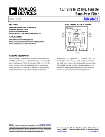
15.1 GHz to 32 GHz, TunableBand-Pass FilterADMV8432Data SheetFEATURESFUNCTIONAL BLOCK DIAGRAMAmplitude settling time: 200 ns typicalWideband rejection: 30 dBSingle chip implementation40-lead, 6 mm 6 mm, RoHS compliant LFCSPAPPLICATIONSADMV8432GNDLOW BANDRFINRFOUTGNDTest and measurement equipmentMilitary radar and electronic warfare (EW) systemsVideo satellite (VSAT) communicationsGNDGNDHIGH BANDVEE GND VDD VCTL GND VTUNE GND20804-001LEVEL SHIFTERFigure 1.GENERAL DESCRIPTIONThe ADMV8432 is a monolithic microwave integrated circuit(MMIC), tunable band-pass filter that features a user selectablepass-band frequency. The 3 dB filter bandwidth is 17% of thecenter frequency (fCENTER). Additionally, fCENTER can be variedbetween 16.6 GHz to 30.1 GHz by applying an analog tuningvoltage between 0 V to 15 V. The usable pass band cornerRev. Afrequencies (fCORNER) span from 15.1 GHz to 32 GHz. Thistunable filter can be used as a much smaller alternative tophysically large switched filter banks and cavity tuned filters.This tunable filter has excellent microphonics due to themonolithic design and provides a dynamically adjustablesolution in advanced communications applications.Document FeedbackInformation furnished by Analog Devices is believed to be accurate and reliable. However, noresponsibility is assumed by Analog Devices for its use, nor for any infringements of patents or otherrights of third parties that may result from its use. Specifications subject to change without notice. Nolicense is granted by implication or otherwise under any patent or patent rights of Analog Devices.Trademarks and registered trademarks are the property of their respective owners.One Technology Way, P.O. Box 9106, Norwood, MA 02062-9106, U.S.A.Tel: 781.329.4700 2019–2021 Analog Devices, Inc. All rights reserved.Technical Supportwww.analog.com
ADMV8432Data SheetTABLE OF CONTENTSFeatures . 1Interface Schematics .7Applications . 1Typical Performance Characteristics .8Functional Block Diagram . 1High Band .8General Description . 1Low Band . 11Revision History . 2High Band and Low Band . 14Specifications. 3Theory of Operation . 15High Band Specifications . 3Applications Information . 16Low Band Specifications. 3Typical Application Circuit . 16DC Characteristics . 4Power Supply Sequence . 16Absolute Maximum Ratings. 5Outline Dimensions . 17ESD Caution . 5Ordering Guide . 17Pin Configuration and Function Descriptions . 6REVISION HISTORY3/2021—Rev. 0 to Rev. AChanges to Product Title and General Description. 1Changes to fCENTER Parameter, Table 1 and 3 dB fCORNERParameter, Table 1. 3Changes to fCENTER Parameter, Table 1 and 3 dB fCORNERParameter, Table 2. 3Changes to Theory of Operation . 157/2019—Revision 0: Initial VersionRev. A Page 2 of 17
Data SheetADMV8432SPECIFICATIONSHIGH BAND SPECIFICATIONSTA 25 C, VDD 5 V, VEE 5 V, and VCTL 0 V, unless otherwise noted.Table 1.ParameterFREQUENCY RANGEfCENTER3 dB fCORNER3 dB Filter ertion LossReturn LossDYNAMIC PERFORMANCEInput Third-Order Intercept (IP3)Input Power at 5 Shift in Insertion PhaseGroup Delay FlatnessPhase SensitivityAmplitude SettlingMinTypMaxUnit30.13217GHzGHz%0.75 fCENTER1.25 fCENTER 40GHzGHzGHz915dBdB37190.10.6200dBmdBmnsRad/Vns 2.7580MHz/ CMHz/V 162dBc/Hz25.723.7Drift RateTuning SensitivityRESIDUAL PHASE NOISE1 MHz OffsetTest Conditions/Comments 30 dB 30 dB 30 dBVTUNE 0 VVTUNE 0 VTime to settle to minimum insertion loss,within 0.5 dB of static insertion lossLOW BAND SPECIFICATIONSTA 25 C, VDD 5 V, VEE 5 V, and VCTL 2.5 V, unless otherwise noted.Table 2.ParameterFREQUENCY RANGEfCENTER3 dB fCORNER3 dB Filter ertion LossReturn LossMinTypMaxUnit22.524.518GHzGHz%0.72 fCENTER1.21 fCENTER 40GHzGHzGHz810dBdB16.615.1Rev. A Page 3 of 17Test Conditions/Comments 30 dB 30 dB 30 dB
ADMV8432ParameterDYNAMIC PERFORMANCEInput IP3Input Power at 5 Shift in Insertion PhaseGroup Delay FlatnessPhase SensitivityAmplitude SettlingData SheetMinDrift RateTuning SensitivityRESIDUAL PHASE NOISE1 MHz OffsetTypMaxUnit34200.150.8200dBmdBmnsRad/Vns 1.4530MHz/ CMHz/V 163dBc/HzTest Conditions/CommentsVTUNE 0 VVTUNE 0 VTime to settle to minimum insertion loss,within 0.5 dB of static insertion lossDC CHARACTERISTICSTable 3.ParameterfCENTER TUNINGVoltage (VTUNE)Current (ITUNE)BAND CONTROL VOLTAGE (VCTL)Input VoltageLowHighCurrentSUPPLY VOLTAGESNegative (VEE)Positive (VDD)SUPPLY CURRENTSNegative (IEE)Positive (IDD)MinTyp002 5.52.5 55MaxUnit15 1VµA0.831VVµA5.5VV1mAmA0.7Rev. A Page 4 of 17Test Conditions/Comments0 V for high band select2.5 V for low band select
Data SheetADMV8432ABSOLUTE MAXIMUM RATINGSTable 4.ParameterTuningVTUNEITUNESupply VoltagesVEEVDDVCTLRF Input Power2 GHz to 50 GHz0.5 GHz to 2 GHz0.1 GHz to 0.5 GHzHot Switch Input Power2 GHz to 50 GHz0.5 GHz to 2 GHz0.1 GHz to 0.5 GHzTemperatureOperatingStorage TemperatureJunction for 1 Million Mean TimesBetween Failures (MTTF)Nominal Junction (TPADDLE 85 C,Input Power (PIN) 23 dBm)Electrostatic Discharge (ESD) RatingHuman Body Model (HBM)Field Induced Charged Device Model(FICDM)Moisture Sensitivity Level (MSL) RatingRating 0.5 V to 15.5 V 1 μA 5.6 V5.6 V 0.5 V to VDD 0.5 VStresses at or above those listed under Absolute MaximumRatings may cause permanent damage to the product. This is astress rating only; functional operation of the product at theseor any other conditions above those indicated in the operationalsection of this specification is not implied. Operation beyondthe maximum operating conditions for extended periods mayaffect product reliability.ESD CAUTION27 dBm19 dBm6 dBm24 dBm16 dBm3 dBm 40 C to 85 C 65 C to 150 C150 C150 C250 V1250 VMSL3Rev. A Page 5 of 17
ADMV8432Data Sheet40393837363534333231NCNCNCNCNCNCNCNCNCNCPIN CONFIGURATION AND FUNCTION DESCRIPTIONS12345678910ADMV8432TOP VIEW(Not to CNOTES1. NC NO CONNECT. THESE PINS ARE NOT CONNECTED INTERNALLY.ALL DATA SHOWN WITHIN WAS MEASURED WITH THESE PINSCONNECTED TO RF AND DCGROUND EXTERNALLY.2. THE EXPOSED PAD IS INTERNALLY CONNECTED TO GROUND.SOLDER THE EXPOSED PAD TO A LOW IMPEDANCE GROUND 314151617181920NCNCNCGNDRFINGNDNCNCNCNCFigure 2. Pin ConfigurationTable 5. Pin Function DescriptionsPin No.1 to 3, 7 to 10, 14, 17, 20 to 24, 28 to 40MnemonicNC4, 6, 12, 16, 18, 25, ptionNo Connect. These pins are not connected internally. All data shown within wasmeasured with these pins connected to RF and dc ground externally.Ground. These pins must be connected to RF and dc ground.RF Input. This pin is dc-coupled and matched to 50 Ω. Blocking capacitors arerequired if the RF line potential is not equal to 0 V.Negative Supply Voltage. VEE is 5 V.Positive Supply Voltage. VDD is 5 V.Control Voltage for Band Selection. The device is in the high band when thevoltage is 0 V and in the low band when the voltage is 2.5 V.Center Frequency Control Voltage of the Band-Pass Filter. VTUNE can be variedfrom 0 V to 15 V.RF Output. This pin is dc-coupled and matched to 50 Ω. Blocking capacitors arerequired if the RF line potential is not equal to 0 V.Exposed Pad. The exposed pad is internally connected to ground. Solder theexposed pad to a low impedance ground plane.Rev. A Page 6 of 17
Data SheetADMV8432INTERFACE SCHEMATICSVDD50Ω20804-003VCTL20804-006RFINFigure 3. VCTL and VDD Interface Schematic0.5nH UNEFigure 6. RFIN Interface SchematicFigure 4. VTUNE Interface SchematicFigure 7. RFOUT Interface Schematic20804-005VEE20804-008GNDFigure 8. GND Interface SchematicFigure 5. VEE Interface SchematicRev. A Page 7 of 17
ADMV8432Data SheetTYPICAL PERFORMANCE CHARACTERISTICSHIGH 250V, S117V, S1115V, S110V, S227V, S2215V, S22–30–60–3505101520253035404550BROADBAND RF FREQUENCY (GHz)–4020804-009–70Figure 9. Insertion Loss vs. Broadband RF Frequency at Various VTUNEVoltages05101520253035404550BROADBAND RF FREQUENCY (GHz)20804-012–20RETURN LOSS (dB)INSERTION LOSS (dB)–10Figure 12. Return Loss vs. Broadband RF Frequency at Various �15–20–250V, S117V, S1115V, S110V, S227V, S2215V, S22–30–14–35–16202530354045RF FREQUENCY (GHz)–401520804-010–1815202530354045RF FREQUENCY (GHz)20804-013RETURN LOSS (dB)INSERTION LOSS (dB)–4Figure 13. Return Loss vs. RF Frequency at Various VoltagesFigure 10. Insertion Loss vs. RF Frequency at Various Voltages–4 85 C 25 C–40 C36 85 C 25 C–40 C–6INSERTION LOSS (dB)34302826–8–10–12–14022012345678910 11 12 13 14 15VTUNE (V)Figure 11. fCENTER vs. VTUNE at Various TemperaturesRev. A Page 8 of 1712345678910 11 12 13 14 15VTUNE (V)Figure 14. Insertion Loss vs. VTUNE at Various Temperatures20804-0142420804-011fCENTER (GHz)32
Data SheetADMV84321.01.41.31.21.11.0012345678910 11 12 13 14 15VTUNE (V)0.90.80.70.60.502345678910 11 12 13 14 15Figure 18. Low-Side Rejection vs. VTUNE at Various Temperatures2445 85 C 25 C–40 C224035181630251420121512345678910 11 12 13 14 15VTUNE (V)1020804-0160 85 C 25 C–40 C012345678910 11 12 13 14 15VTUNE (V)Figure 16. 3 dB Bandwidth vs. VTUNE at Various Temperatures20804-019INPUT IP3 (dBm)2010Figure 19. Input IP3 vs. VTUNE at Various Temperatures12000.7 85 C 25 C–40 C1100 85 C 25 C–40 C0.61000GROUP DELAY 10 11 12 13 14 15VTUNE (V)Figure 17. Tuning Sensitivity vs. VTUNE at Various Temperatures0012345678910 11 12 13 14 15VTUNE (V)Figure 20. Group Delay vs. VTUNE at Various TemperaturesRev. A Page 9 of 1720804-02030020804-017TUNING SENSITIVITY (MHz/V)1VTUNE (V)Figure 15. High-Side Rejection vs. VTUNE at Various Temperatures3dB BANDWIDTH (%) 85 C 25 C–40 C20804-018LOW-SIDE REJECTION RATIO (dB) 85 C 25 C–40 C20804-015HIGH-SIDE REJECTION RATIO (dB)1.5
ADMV8432Data Sheet–1000.50.40.322242628303234363840RF FREQUENCY ATE fCENTER (GHz)PHASE SENSITIVITY (Rad/V)3V15VAPPROXIMATE fCENTER (GHz)1050–5–152468101214161820INPUT POWER (dBm)20804-022–10010MFigure 23. Residual Phase Noise vs. Offset Frequency at Various VTUNEVoltages150V7V1MOFFSET FREQUENCY (Hz)Figure 21. Group Delay vs. RF Frequency at Various VTUNE VoltagesPHASE SHIFT (Degrees)–130–17010020804-0210.220–120Figure 22. Phase Shift vs. Input Power at Various VTUNE Voltages301.6281.2260.8240.4220123456789010 11 12 13 14 15VTUNE (V)Figure 24. Approximate fCENTER and Phase Sensitivity vs. VTUNERev. A Page 10 of 17PHASE SENSITIVITY (Rad/V)GROUP DELAY (ns)0.60V7V15V–11020804-023RESIDUAL PHASE NOISE (dBc/Hz)0V7V15V20804-0240.7
Data SheetADMV8432LOW BAND000V7V15V–5–10–30–40–50–20–250V, S117V, S1115V, S110V, S227V, S2215V, S22–30–60–3505102015253035404550BROADBAND RF FREQUENCY AND RF FREQUENCY (GHz)Figure 25. Insertion Loss vs. Broadband RF Frequency for Various VTUNEVoltagesFigure 28. Return Loss vs. Broadband RF Frequency for Various VTUNEVoltages000V7V15V–2–5–4–10RETURN LOSS (dB)–6–8–10–12–15–20–250V, S117V, S1115V, S110V, S227V, S2215V, S22–30–14–35–165101520253035RF FREQUENCY (GHz)–4020804-026–18Figure 26. Insertion Loss vs. RF Frequency for Various VTUNE Voltages51020152520804-029INSERTION LOSS (dB)–1520804-028–20RETURN LOSS (dB)INSERTION LOSS (dB)–103530RF FREQUENCY (GHz)Figure 29. Return Loss vs. RF Frequency for Various VTUNE Voltages–426 85 C 25 C–40 C 85 C 25 C–40 C24INSERTION LOSS (dB)–6201816–8–10–1212012345678910 11 12 13 14 15VTUNE (V)–14012345678910 11 12 13 14 15VTUNE (V)Figure 30. Insertion Loss vs. VTUNE at Various TemperaturesFigure 27. fCENTER vs. VTUNE at Various TemperaturesRev. A Page 11 of 1720804-0301420804-027fCENTER (GHz)22
ADMV8432Data Sheet1.01.41.31.21.11.0012345678910 11 12 13 14 15VTUNE (V)0.90.80.70.60.502345678910 11 12 13 14 15Figure 34. Low-Side Rejection vs. VTUNE at Various Temperatures2445 85 C 25 C–40 C224035181630251420121512345678910 11 12 13 14 15VTUNE (V)1020804-0320 85 C 25 C–40 C012345678910 11 12 13 14 15VTUNE (V)Figure 32. 3 dB Bandwidth vs. VTUNE at Various Temperatures20804-035INPUT IP3 (dBm)2010Figure 35. Input IP3 vs. VTUNE at Various Temperatures12000.7 85 C 25 C–40 C1100 85 C 25 C–40 C0.61000GROUP DELAY 10 11 12 13 14 15VTUNE (V)Figure 33. Tuning Sensitivity vs. VTUNE at Various Temperatures0012345678910 11 12 13 14 15VTUNE (V)Figure 36. Group Delay vs. VTUNE at Various TemperaturesRev. A Page 12 of 1720804-03630020804-033TUNING SENSITIVITY (MHz/V)1VTUNE (V)Figure 31. High-Side Rejection vs. VTUNE at Various Temperatures3dB BANDWIDTH (%) 85 C 25 C–40 C20804-034LOW-SIDE REJECTION RATIO (dB) 85 C 25 C–40 C20804-031HIGH-SIDE REJECTION RATIO (dB)1.5
Data SheetADMV8432–1000.50.40.312141618202224262830RF FREQUENCY ATE fCENTER (GHz)PHASE SENSITIVITY (Rad/V)3V15VAPPROXIMATE fCENTER (GHz)1050–5–152468101214161820INPUT POWER (dBm)20804-038–10010MFigure 39. Residual Phase Noise vs. Offset Frequency at Various VTUNEVoltages150V7V1MOFFSET FREQUENCY (Hz)Figure 37. Group Delay vs. RF Frequency at Various VTUNE VoltagesPHASE SHIFT 01.2180.8160.414Figure 38. Phase Shift vs. Input Power at Various VTUNE Voltages0123456789010 11 12 13 14 15VTUNE (V)Figure 40. Approximate fCENTER and Phase Sensitivity vs. VTUNERev. A Page 13 of 17PHASE SENSITIVITY (Rad/V)GROUP DELAY (ns)0.60V7V15V–11020804-039RESIDUAL PHASE NOISE (dBc/Hz)0V7V15V20804-0400.7
ADMV8432Data SheetHIGH BAND AND LOW BAND36–4HIGH BANDLOW BAND34HIGH BANDLOW BAND32–6INSERTION LOSS (dB)30fCENTER (GHz)282624222018–8–10–1216012345678910 11 12 13 14 15VTUNE (V)–1420804-041120Figure 41. fCENTER vs. VTUNE–30–40–50–60–701015202530354045RF FREQUENCY (GHz)5020804-042BROADBAND INSERTION LOSS (dB)–205345678910 11 12 13 14 15Figure 43. Insertion Loss vs. VTUNEHIGH BAND, 0VHIGH BAND, 7VHIGH BAND, 15VLOW BAND, 0VLOW BAND, 7VLOW BAND, 15V02VTUNE (V)0–101Figure 42. Broadband Insertion Loss vs. RF FrequencyRev. A Page 14 of 1720804-04314
Data SheetADMV8432THEORY OF OPERATIONThe ADMV8432 is a MMIC, band-pass filter that features auser selectable pass-band frequency. To select the high band,apply 0 V at VCTL, and to select the low band, apply 2.5 V atVCTL. Varying the applied analog tuning voltage between 0 Vand 15 V at VTUNE varies the fCENTER from 16.6 GHz to 22.5 GHzfor the low band and from 25.7 GHz to 30.1 GHz for the highband.Rev. A Page 15 of 17
ADMV8432Data SheetTHRU CAL1J24 3 2DNI4 3 2DNIAGNDAGNDJ31 RFIN4 3 OUTADMV8432 GNDNCNCNCNC30292827262524232221RFOUT1J44 3 3534333231APPLICATIONS C31000pFAGNDAGND1VDDRED UNEGRNC7 4.7µFAGNDVBWORGDNIC10 4.7µFDNIAGND20804-044R210kΩDNIAGNDFigure 44. Typical Application CircuitTYPICAL APPLICATION CIRCUITPOWER SUPPLY SEQUENCEFigure 44 shows the typical application circuit for theADMV8432.The required power-up sequence is GND, VDD, VEE, VCTL,and VTUNE. Deviations from this sequence may forward biasthe ESD protection structures and damage them.Rev. A Page 16 of 17
Data SheetADMV8432OUTLINE DIMENSIONSDETAIL A(JEDEC 95)6.106.00 SQ5.900.300.250.20311300.50BSCTOP VIEW0.800.750.70SIDE VIEWPKG-006061SEATINGPLANE*0.350.300.25P IN 1IN D IC ATO R AR E A OP T IO N S(SEE DETAIL A)404.754.70 SQ4.65EXPOSEDPAD2111200.05 MAX0.02 NOMCOPLANARITY0.080.20 REFBOTTOM VIEW100.20 MIN4.50 REFFOR PROPER CONNECTION OFTHE EXPOSED PAD, REFER TOTHE PIN CONFIGURATION ANDFUNCTION DESCRIPTIONSSECTION OF THIS DATA SHEET.*COMPLIANT TO JEDEC STANDARDS MO-220-WJJD-5WITH EXCEPTION TO LEAD LENGTH01-29-2019-APIN 1INDICATORAREAFigure 45. 40-Lead Lead Frame Chip Scale Package [LFCSP]6 mm 6 mm Body and 0.75 mm Package Height(CP-40-27)Dimensions shown in millimetersORDERING LZ1Temperature Range 40 C to 85 C 40 C to 85 CPackage Description40-Lead Lead Frame Chip Scale Package [LFCSP]40-Lead Lead Frame Chip Scale Package [LFCSP]Evaluation BoardZ RoHS Compliant Part. 2019–2021 Analog Devices, Inc. All rights reserved. Trademarks andregistered trademarks are the property of their respective owners.D20804-3/21(A)Rev. A Page 17 of 17Package OptionCP-40-27CP-40-27
center frequency (f CENTER). Additionally, f CENTER can be varied between 16.6 GHz to 30.1 GHz by applying an analog tuning voltage between 0 V to 15 V. The usable pass band corner frequencies (f CORNER) span from 15.1 GHz to 32 GHz. This tunable filter can be used as a much smaller alternative to