Transcription
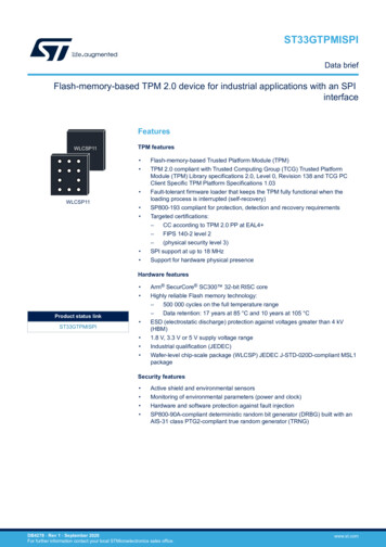
ST33GTPMISPIData briefFlash-memory-based TPM 2.0 device for industrial applications with an SPIinterfaceFeaturesWLCSP11TPM features WLCSP11 Flash-memory-based Trusted Platform Module (TPM)TPM 2.0 compliant with Trusted Computing Group (TCG) Trusted PlatformModule (TPM) Library specifications 2.0, Level 0, Revision 138 and TCG PCClient Specific TPM Platform Specifications 1.03Fault-tolerant firmware loader that keeps the TPM fully functional when theloading process is interrupted (self-recovery)SP800-193 compliant for protection, detection and recovery requirementsTargeted certifications:–CC according to TPM 2.0 PP at EAL4 –FIPS 140-2 level 2–(physical security level 3)SPI support at up to 18 MHzSupport for hardware physical presenceHardware features Product status linkST33GTPMISPI Arm SecurCore SC300 32-bit RISC coreHighly reliable Flash memory technology:–500 000 cycles on the full temperature range–Data retention: 17 years at 85 C and 10 years at 105 CESD (electrostatic discharge) protection against voltages greater than 4 kV(HBM)1.8 V, 3.3 V or 5 V supply voltage rangeIndustrial qualification (JEDEC)Wafer-level chip-scale package (WLCSP) JEDEC J-STD-020D-compliant MSL1packageSecurity features Active shield and environmental sensorsMonitoring of environmental parameters (power and clock)Hardware and software protection against fault injectionSP800-90A-compliant deterministic random bit generator (DRBG) built with anAIS-31 class PTG2-compliant true random generator (TRNG)DB4278 - Rev 1 - September 2020For further information contact your local STMicroelectronics sales office.www.st.com
ST33GTPMISPI Cryptographic algorithms:–RSA key generation (1024 or 2048 bits)–RSA signature (RSASSA-PSS, RSASSA-PKCS1v1 5)–RSA encryption (RSAES-OAEP, RSAESPKCS1-v1 5)–SHA-1, SHA-2 (256 and 384 bits), SHA-3 (256 and 384 bits)–HMAC SHA-1, SHA-2 and SHA-3–AES-128,192 and 256 bits–TDES 192 bits–ECC (NIST P-256, P-384 curves): key generation, ECDH and ECDSA,ECSchnorr–ECDAA (BN-256 curve)–Device provided with 3 endorsement keys (EK) and EK certificates(RSA2048, ECC NIST P 256 and ECC NIST P 384)–Device provisioned with 3 RSA key pairs to reduce the TPM provisioningtimeProduct compliance DB4278 - Rev 1Compliant with TCG test suite for TPM 2.0Common Criteria certifications:–EAL 4 on TCG TPM2.0 protection profile–EAL 5 on hardwareTargets FIPS 140-2 level 2 certification (physical security level 3)page 2/22
ST33GTPMISPIDescription1DescriptionThe ST33GTPMISPI is a cost-effective and high-performance trusted platform module (TPM) targeting industrialembedded systems.The product implements the functions defined by the Trusted Computing Group (www.trustedcomputinggroup.org)in the TCG Trusted Platform Module Library Specifications version 2.0 Level 0 Revision 138 ([TPM 2.0 P1 r138],[TPM 2.0 P2 r138], [TPM 2.0 P3 r138], [TPM 2.0 P4 r138]) and errata version 1.4 [TPM 2.0 rev138 Err 1.4]. It isalso based on the TCG PC client-specific TPM Platform specifications rev1.03 [PTP 2.0 r1.03]. The applicableprotection profile is TCG Protection Profile for PC Client Specific TPM 2.0 ([TPM 2.0 PP]).The product also supports the ability to upgrade the TPM firmware thanks to a persistent Flash memory loaderapplication to support new standard evolutions.1.1Security certificationsThis product is CC certified according to TPM 2.0 PP at EAL4 .1.2Hardware featuresThe ST33GTPMISPI is based on a smartcard-class secure MCU that incorporates the most recent generation ofArm processors for embedded secure systems. Its SecurCore SC300 32-bit RISC core is built on theCortex -M3 core with additional security features to help to protect against advanced forms of attack.The ST33GTPMISPI offers a fast slave serial peripheral interface (SPI) supported by an embeddedcommunication engine compliant with TCG PC client TPM Profile 1.03 [PTP 2.0 r1.03].The product features hardware accelerators for advanced cryptographic functions. The AES peripheral provides asecure AES (Advanced Encryption Standard) algorithm implementation, while the NESCRYPT cryptoprocessorefficiently supports public-key algorithms.The ST33GTPMISPI comes in the WLCSP11 ECOPACK-compliant package. ECOPACK is an ST trademark.Note:DB4278 - Rev 1Arm is a registered trademark of Arm Limited (or its subsidiaries) in the US and/or elsewhere.page 3/22
ST33GTPMISPIPin and signal descriptions2Pin and signal descriptionsThe figure below gives the pinout of the WLCSP11 package in which the devices are delivered. The tabledescribes the associated signals.Figure 1. WLCSP11 pinout (top view)3Bump side view21AGNDSPI MISO VPSPin A1 markerBGPIO LP NiCSPI MOSICGPIO PPSPI CLKDSPI CS SPI PIRQ SPI RSTTable 1. Pin descriptionsSignalTypeDescriptionGPIO PPInputPhysical Presence, active high, internal pull-down. Used to indicate Physical Presence to the TPMdevice. The GPIO function could be modified by activating the GPIOs mapped with the NV storage indexfeature.VPSInputPower supply. This pin must be connected to 1.8 V or 3.3 V DC power rail supplied by the motherboard.GNDInputGND has to be connected to the main motherboard ground.SPI RSTInputSPI Reset active low, used to re-initialize the device. Must not be unconnected. External pull-up requiredif the pin cannot be driven.SPI MISO Output SPI Master Input, Slave Output (output from slave)SPI MOSI InputSPI Master Output, Slave Input (output from master)SPI CLKInputSPI Serial Clock (output from master)SPI CSInputSPI Chip (or Slave) Select, internal pull-up (active low; output from master)SPI PIRQ Output SPI IRQ active low, open drain, used by the TPM to generate an interrupt.DB4278 - Rev 1NiC-GPIO LP-Not internally connected: not connected to the die. May be left unconnected but no impact on the TPMdevice if connected.By default: Used for activation and deactivation of the TPM Standby mode (TPMLowPowerByGpio).The GPIO function could be modified by activating the GPIOs mapped with the NV storage index feature.page 4/22
ST33GTPMISPIIntegration guidance3Integration guidance3.1Typical hardware implementationThe Physical Presence (PP) pin should be connected if platform implementation (at boot level) uses a hardwarephysical presence function.The figure below shows the hardware implementation for the WLCSP11 package.Figure 2. Typical hardware implementation (WLCSP11 package)321SPI MISOVPSGNDAGNDGPIO LPSPI MISO VPSSPI MOSIBGPIO LP NiCGPIO PP100 nF10 µFSPI MOSISPI CLKCSPI CLKGPIO PPSPI PIRQSPI CSSPI RSTDSPI CSSPI RSTSPI PIRQDB4278 - Rev 1page 5/22
ST33GTPMISPIPower supply filtering3.2Power supply filteringThe power supply of the circuit must be filtered using the circuit shown in the figure below.Figure 3. Mandatory filtering capacitors on VPSHost deviceSPI MISOSPI MOSISPI CLKSPI RSTSPI CSSPI PIRQVPS10 µF TPM100 nFGND1.10 µF and 100 nF are recommended values. The minimum required capacitor value is 2.1 µF (2 µF inparallel with 100 nF).Table 2. Maximum VPS rising slopeSymbolSVPSDB4278 - Rev 1ParameterMaximum VPS rising slopeValue5UnitV/µspage 6/22
ST33GTPMISPIPackage information4Package informationIn order to meet environmental requirements, ST offers these devices in different grades of ECOPACK packages,depending on their level of environmental compliance. ECOPACK specifications, grade definitions and productstatus are available at: www.st.com. ECOPACK is an ST trademark.4.1WLCSP11 package informationWLCSP11 stands for 2.549 2.745 mm 11-bump wafer-level chip-scale package.Figure 4. WLCSP11 – package outlineDXbbb Ze2GYA1 bump cornerFDETAIL AEe1e1mil BSPFaaaAA2WAFER BACK SIDESIDE VIEWNOTCHeGBUMP SIDEBUMPA1eee ZZ(Note 2) b(11x)ccc Z X Yddd Z(Note 4)1.2.3.4.DB4278 - Rev 1DETAIL AROTATED 90 SEATING PLANE(Note 3)Dimensions and tolerance as per ASME Y 14.5M - 1994.Dimension is measured at the maximum bump diameter parallel to primary datum Z.Primary datum Z and seating plane are defined by the spherical crowns of the bump.Bump position designation per JESD 95-1, SPP-010.page 7/22
ST33GTPMISPIPCB design and reflow recommendationsTable 3. WLCSP11 - package mechanical dataInches 43-ddd-0.060--0.0024-eee-0.060--0.0024-1. Values in inches are converted from mm and rounded to 4 decimal digits.2. N is the total number of terminals.4.2PCB design and reflow recommendationsThe recommendations provided in this section apply to the WLCSP package only and must be considered asdevelopment guidance for PCB designer. It is linked to ST's package development and qualification procedure; asa result it must be fine-tuned and adapted according to customer process.DB4278 - Rev 1page 8/22
ST33GTPMISPIPCB design and reflow recommendationsFigure 5. PCB landing patternSolder mask openingSolder pad widthCopper trace widthSolder mask widthCopper trace thicknessTable 4. PCB design parametersParameterValueSolder pad width230 µmSolder mask opening345 µmSolder mask thickness25 µmCopper trace thickness30 µmCopper trace width80 µmThis package is compliant with the IPC/JEDEC J-STD-020D specifications.The ST WLCSP is ECOPACK compliant: In order to meet environmental requirements, ST offers ECOPACKpackages. These packages have a lead-free second-level interconnect. The category of second-levelinterconnect is marked on the package and on the inner box label, in compliance with JEDEC Standard JESD97.The maximum ratings related to soldering conditions are also marked on the inner box label. ECOPACK is an STtrademark. ECOPACK specifications are available at www.st.com.DB4278 - Rev 1page 9/22
ST33GTPMISPIWLCSP tape and reel packingFigure 6. Reflow soldering temperature profileThe previous figure shows the reflow soldering temperature profile ( C versus time) and the table below providesthe critical reflow parameters (typical values).Table 5. Critical reflow parametersParameter4.3Value (typical)Process step Lead-free solder: Ramp rate3 C/sPre-heat150 C to 180 C, 60 to 180 secondsTime above liquidus (TAL)220 C, 30 to 90 secondsPeak temperature255 C 5 CTime within 5 C of peak temperature10 to 20 secondsRamp-down rate6 C/s maximumWLCSP tape and reel packingSurface-mount packages can be supplied with tape and reel packing.Reels are in plastic, either antistatic or conductive, with a black conductive cavity tape. The cover tape istransparent antistatic or conductive.The devices are positioned in the cavities with the identifying pin (normally Pin “A1”) on the same side as thesprocket holes in the tape.The STMicroelectronics tape and reel specifications are compliant to the EIA 481-A standard specification.Table 6. WLCSPs on tape and reelDB4278 - Rev 1PackageQuantity per reel11-bump, wafer-level chip-scale package (WLCSP)5000page 10/22
ST33GTPMISPIWLCSP tape and reel packingFigure 7. WLCSP11 reel diagramW2BANCDW1Table 7. WLCSP11 reel dimensionsAll dimensions except for the reel diameter are in millimeters.Reel diameterABCDNW1(1)W1W2W113 inches330 (typ.)2.2 ( 0.5)13 ( 0.25)20.2 (min.)4 inches12.4 ( 2, 0)18.4 (max.)1. Measured at hub.Figure 8. WLCSP11 leader and trailerDB4278 - Rev 1page 11/22
ST33GTPMISPIWLCSP tape and reel packingFigure 9. Embossed carrier tape for WLCSP11P1Ø D0P2 (see note 2)Ø D1P0 (see note 1)ABoBEAFWR 0.79 0.10KoBSection B-B0.19 0.100.79 0.10Detail(2 )AomSection A-A(45 )Detail1.2.3.4.5.Cumulative tolerance of the sprocket hole pitch is 0.2.Pocket position relative to sprocket hole measured as the true position of the pocket, not the pocket hole.Ao and Bo are measured on a plane at a distance R above the bottom of the pocket.Drawing is not to scale.Dimensions are in millimeters.Table 8. Carrier tape dimensions for WLCSP11DB4278 - Rev 1D0D1EFm (max) Ko1.50 0.1/–0.01.00 0.1/–0.01.75 0.105.50 0.05 0.250.72 0.05AoBoP0P1P2W2.71 0.052.91 0.054.00 0.18.00 0.12.00 0.0512.00 0.3/–0.1page 12/22
ST33GTPMISPIPackage marking information5Package marking informationParts marked as E or ES (for engineering sample) are not yet qualified and therefore not approved for use inproduction. ST is not responsible for any consequences resulting from such use. In no event will ST be liable forthe customer using any of these engineering samples in production. ST’s Quality department must be contactedprior to any decision to use these engineering samples to run a qualification activity.Figure 10. WLCSP11 standard marking exampleABDCGEFHLegend:A: Marking area – 8 digitsE: Assembly weekB: Marking area – 8 digitsF: Assembly plantC: BE sequenceG: Dot(1)D: Assembly yearH: Marking area – 5 digits1. The dot on the back side indicates the A1 ball location.DB4278 - Rev 1page 13/22
ST33GTPMISPIOrdering information6Ordering informationTable 9. Ordering information for products supporting firmware 0x00 0x03 0x01 0x01 (0x0003.0x0101) (3.257) preloadedin factoryOrdering codeFirmware versionOperating temperaturerangeMaximum SPI clockfrequencyPackageA marking B markingareaarea0x00 0x03 0x01 0x01ST33GTPMIWLFZE4DB4278 - Rev 1(0x0003 0x0101)(3.257) 40 C to 105 C18 MHzWLCSP11GTPMISPIFZE4page 14/22
ST33GTPMISPISupport and information7Support and informationAdditional information regarding ST TPM devices can be obtained from the www.st.com website.For any specific support information you can contact STMicroelectronics through the following e-mail:TPMsupport@list.st.com.DB4278 - Rev 1page 15/22
ST33GTPMISPITerms and abbreviationsAppendix A Terms and abbreviationsTable 10. List of abbreviationsTermDB4278 - Rev 1MeaningAESAdvanced Encryption StandardCACertificate authorityCCCommon CriteriaDRBGDeterministic random-bit generatorDAMDictionary attack mitigation mechanismData byteByte from the TPM command or answer or register value.DESData Encryption StandardECElliptic curveECDAAElliptic curve direct anonymous attestation (algorithm)ECDHElliptic curve Diffie–HellmanEKEndorsement keyFIPSFederal Information Processing StandardGPIOGeneral-purpose I/OHMACKeyed-Hashing for message authenticationHSMHardware security moduleNISTNational Institute of Standards and TechnologyNVNon-volatile (memory)OEMOriginal equipment manufacturerOIAPObject-independent authorization protocolOSAPObject-specific authorization protocolPCRPlatform Configuration RegisterRSARivest Shamir AdelmanRTMRoot of trust for measurementRTRRoot of trust for reportingSHASecure Hash algorithmSPISerial Peripheral InterfaceSRKStorage root keyTCGTrusted Computed GroupTISTPM interface specificationTPMTrusted Platform ModuleTRNGTrue random-number generatorTPMETPM manufacturerTransaction bytesAll bytes from a TPM command or TPM answer.TSSTPM software stackpage 16/22
ST33GTPMISPIReferenced documentsAppendix B Referenced documentsThe following materials are to be used in conjunction with this document, or are referenced in it.[TPM 2.0 P1 r138]TPM Library, Part 1, Architecture, Family 2.0, rev 1.38, TCG[TPM 2.0 P2 r138]TPM Library, Part 2, Structures, Family 2.0, rev 1.38, TCG[TPM 2.0 P3 r138]TPM Library, Part 3, Commands, Family 2.0, rev 1.38, TCG[TPM 2.0 P4 r138]TPM Library, Part 4, Supporting routines, Family 2.0, rev 1.38, TCG[TPM 2.0 rev138 Err 1.4] TPM Library, Family 2.0, rev 1.38, Errata 1.4, January 8, 2018, TCG.DB4278 - Rev 1[PTP 2.0 r1.03]TCG PC Client Specific Platform TPM Specification (PTP) - Version 2.0 Revision 1.03[PKCS#1]PKCS#1: v2.1 RSA Cryptography Standard, RSA Laboratories[AN2639]Application note, Soldering recommendations and package information for Lead-free ECOPACK microcontrollers, STMicroelectronics[TPM 20 PP]Protection Profile PC Client Specific TPM, Family 2.0 Level 0 revision 1.38 (1.1), TCG.page 17/22
ST33GTPMISPIRevision historyTable 11. Document revision historyDB4278 - Rev 1DateVersion07-Sep-20201ChangesInitial release.page 18/22
ST33GTPMISPIContentsContents1Description . . . . . . . . . . . . . . . . . . . . . . . . . . . . . . . . . . . . . . . . . . . . . . . . . . . . . . . . . . . . . . . . . . . . . . . .31.1Security certifications . . . . . . . . . . . . . . . . . . . . . . . . . . . . . . . . . . . . . . . . . . . . . . . . . . . . . . . . . . . 31.2Hardware features. . . . . . . . . . . . . . . . . . . . . . . . . . . . . . . . . . . . . . . . . . . . . . . . . . . . . . . . . . . . . . 32Pin and signal description . . . . . . . . . . . . . . . . . . . . . . . . . . . . . . . . . . . . . . . . . . . . . . . . . . . . . . . . . 43Integration guidance. . . . . . . . . . . . . . . . . . . . . . . . . . . . . . . . . . . . . . . . . . . . . . . . . . . . . . . . . . . . . . . 543.1Typical hardware implementation . . . . . . . . . . . . . . . . . . . . . . . . . . . . . . . . . . . . . . . . . . . . . . . . . 53.2Power supply filtering . . . . . . . . . . . . . . . . . . . . . . . . . . . . . . . . . . . . . . . . . . . . . . . . . . . . . . . . . . . 6Package information. . . . . . . . . . . . . . . . . . . . . . . . . . . . . . . . . . . . . . . . . . . . . . . . . . . . . . . . . . . . . . .74.1WLCSP11 package information. . . . . . . . . . . . . . . . . . . . . . . . . . . . . . . . . . . . . . . . . . . . . . . . . . . 74.2PCB design and reflow recommendations . . . . . . . . . . . . . . . . . . . . . . . . . . . . . . . . . . . . . . . . . . 84.3WLCSP tape and reel packing. . . . . . . . . . . . . . . . . . . . . . . . . . . . . . . . . . . . . . . . . . . . . . . . . . . 105Package marking information . . . . . . . . . . . . . . . . . . . . . . . . . . . . . . . . . . . . . . . . . . . . . . . . . . . . .136Ordering information . . . . . . . . . . . . . . . . . . . . . . . . . . . . . . . . . . . . . . . . . . . . . . . . . . . . . . . . . . . . .147Support and information . . . . . . . . . . . . . . . . . . . . . . . . . . . . . . . . . . . . . . . . . . . . . . . . . . . . . . . . . .15Appendix A Terms and abbreviations . . . . . . . . . . . . . . . . . . . . . . . . . . . . . . . . . . . . . . . . . . . . . . . . .16Appendix B Referenced documents . . . . . . . . . . . . . . . . . . . . . . . . . . . . . . . . . . . . . . . . . . . . . . . . . .17Revision history . . . . . . . . . . . . . . . . . . . . . . . . . . . . . . . . . . . . . . . . . . . . . . . . . . . . . . . . . . . . . . . . . . . . . . .18Contents . . . . . . . . . . . . . . . . . . . . . . . . . . . . . . . . . . . . . . . . . . . . . . . . . . . . . . . . . . . . . . . . . . . . . . . . . . . . . .19List of tables . . . . . . . . . . . . . . . . . . . . . . . . . . . . . . . . . . . . . . . . . . . . . . . . . . . . . . . . . . . . . . . . . . . . . . . . . .20List of figures. . . . . . . . . . . . . . . . . . . . . . . . . . . . . . . . . . . . . . . . . . . . . . . . . . . . . . . . . . . . . . . . . . . . . . . . . .21DB4278 - Rev 1page 19/22
ST33GTPMISPIList of tablesList of tablesTable 1.Table 2.Table 3.Table 4.Table 5.Table 6.Table 7.Table 8.Table 9.Table 10.Table 11.Pin descriptions . . . . . . . . . . . . . . . . . . . . . . . . . . . . . . . . . . . . . . . . . . . . . . . . . . . . . . . . . . . . . . . . . . . . . 4Maximum VPS rising slope . . . . . . . . . . . . . . . . . . . . . . . . . . . . . . . . . . . . . . . . . . . . . . . . . . . . . . . . . . . . . 6WLCSP11 - package mechanical data . . . . . . . . . . . . . . . . . . . . . . . . . . . . . . . . . . . . . . . . . . . . . . . . . . . . . 8PCB design parameters . . . . . . . . . . . . . . . . . . . . . . . . . . . . . . . . . . . . . . . . . . . . . . . . . . . . . . . . . . . . . . . 9Critical reflow parameters . . . . . . . . . . . . . . . . . . . . . . . . . . . . . . . . . . . . . . . . . . . . . . . . . . . . . . . . . . . . . 10WLCSPs on tape and reel. . . . . . . . . . . . . . . . . . . . . . . . . . . . . . . . . . . . . . . . . . . . . . . . . . . . . . . . . . . . . 10WLCSP11 reel dimensions . . . . . . . . . . . . . . . . . . . . . . . . . . . . . . . . . . . . . . . . . . . . . . . . . . . . . . . . . . . . 11Carrier tape dimensions for WLCSP11 . . . . . . . . . . . . . . . . . . . . . . . . . . . . . . . . . . . . . . . . . . . . . . . . . . . . 12Ordering information for products supporting firmware 0x00 0x03 0x01 0x01 (0x0003.0x0101) (3.257) preloaded infactory . . . . . . . . . . . . . . . . . . . . . . . . . . . . . . . . . . . . . . . . . . . . . . . . . . . . . . . . . . . . . . . . . . . . . . . . . . 14List of abbreviations . . . . . . . . . . . . . . . . . . . . . . . . . . . . . . . . . . . . . . . . . . . . . . . . . . . . . . . . . . . . . . . . . 16Document revision history . . . . . . . . . . . . . . . . . . . . . . . . . . . . . . . . . . . . . . . . . . . . . . . . . . . . . . . . . . . . . 18DB4278 - Rev 1page 20/22
ST33GTPMISPIList of figuresList of figuresFigure 1.Figure 2.Figure 3.Figure 4.Figure 5.Figure 6.Figure 7.Figure 8.Figure 9.Figure 10.DB4278 - Rev 1WLCSP11 pinout (top view) . . . . . . . . . . . . . . . . . . .Typical hardware implementation (WLCSP11 package)Mandatory filtering capacitors on VPS . . . . . . . . . . . .WLCSP11 – package outline . . . . . . . . . . . . . . . . . .PCB landing pattern . . . . . . . . . . . . . . . . . . . . . . . .Reflow soldering temperature profile . . . . . . . . . . . . .WLCSP11 reel diagram . . . . . . . . . . . . . . . . . . . . . .WLCSP11 leader and trailer . . . . . . . . . . . . . . . . . . .Embossed carrier tape for WLCSP11. . . . . . . . . . . . .WLCSP11 standard marking example . . . . . . . . . . . . 4. 5. 6. 7. 91011111213page 21/22
ST33GTPMISPIIMPORTANT NOTICE – PLEASE READ CAREFULLYSTMicroelectronics NV and its subsidiaries (“ST”) reserve the right to make changes, corrections, enhancements, modifications, and improvements to STproducts and/or to this document at any time without notice. Purchasers should obtain the latest relevant information on ST products before placing orders. STproducts are sold pursuant to ST’s terms and conditions of sale in place at the time of order acknowledgement.Purchasers are solely responsible for the choice, selection, and use of ST products and ST assumes no liability for application assistance or the design ofPurchasers’ products.No license, express or implied, to any intellectual property right is granted by ST herein.Resale of ST products with provisions different from the information set forth herein shall void any warranty granted by ST for such product.ST and the ST logo are trademarks of ST. For additional information about ST trademarks, please refer to www.st.com/trademarks. All other product or servicenames are the property of their respective owners.Information in this document supersedes and replaces information previously supplied in any prior versions of this document. 2020 STMicroelectronics – All rights reservedDB4278 - Rev 1page 22/22
TPM features Flash-memory-based Trusted Platform Module (TPM) TPM 2.0 compliant with Trusted Computing Group (TCG) Trusted Platform Module (TPM) Library specifications 2.0, Level 0, Revision 138 and TCG PC Client Specific TPM Platform Specifications 1.03 Fault-tolerant firmware loader that keeps the TPM fully functional when the