Transcription
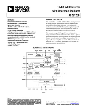
12-Bit R/D Converterwith Reference OscillatorAD2S1200FEATURESGENERAL DESCRIPTIONComplete monolithic R/D converterParallel and serial 12-bit data portsSystem fault detectionAbsolute position and velocity outputsDifferential inputs 11 arc minutes of accuracy1,000 rps maximum tracking rate, 12-bit resolutionIncremental encoder emulation (1,024 pulses/rev)Programmable sinusoidal oscillator on-boardCompatible with DSP and SPI interface standards204.8 kHz square wave outputSingle-supply operation (5.00 V 5%) 40 C to 125 C temperature rating44-lead LQFP package4 kV ESD protectionThe AD2S1200 is a complete 12-bit resolution tracking resolverto-digital converter, integrating an on-board programmablesinusoidal oscillator that provides sine wave excitation forresolvers. An external 8.192 MHz crystal is required to providea precision time reference. This clock is internally divided togenerate a 4.096 MHz clock to drive all the peripherals.The converter accepts 3.6 V p-p 10% input signals, in therange of 10 kHz to 20 kHz on the Sin and Cos inputs. A Type IIservo loop is employed to track the inputs and convert the inputSin and Cos information into a digital representation of theinput angle and velocity. The bandwidth of the converter is setinternally to 1.7 kHz with an external 8.192 MHz crystal. Themaximum tracking rate is 1,000 rps.FUNCTIONAL BLOCK DIAGRAMREFBYPAD2S1200REFOUTFS1CLKINXTALOUT LOSinADCANGLE ERRORMONITORADCDIGITALFILTERANGLE NTEGRATORVELOCITYINTEGRATORPOSITION REGISTERVELOCITY B10SCLKDB9–DB0CSRD04406-0-001DATA BUS OUTPUTFigure 1.Rev. 0Information furnished by Analog Devices is believed to be accurate and reliable.However, no responsibility is assumed by Analog Devices for its use, nor for anyinfringements of patents or other rights of third parties that may result from its use.Specifications subject to change without notice. No license is granted by implicationor otherwise under any patent or patent rights of Analog Devices. Trademarks andregistered trademarks are the property of their respective owners.One Technology Way, P.O. Box 9106, Norwood, MA 02062-9106, U.S.A.Tel: 781.329.4700www.analog.comFax: 781.326.8703 2003 Analog Devices, Inc. All rights reserved.
AD2S1200APPLICATIONSElectric power steeringElectric vehiclesIntegrated starter generator/alternatorEncoder emulationAutomotive motion sensing and control Triple Format Position Data: Absolute 12-bit angularbinary position data accessed either via a 12-bit parallelport or via a 3-wire serial interface. Incremental encoderemulation in standard A QUAD B format, with directionoutput is available. Digital Velocity Output: 12-bit signed digital velocity,twos complement format, accessed either via a 12-bitparallel port or via a 3-wire serial interface. Programmable Excitation Frequency: Excitation frequency easily programmable to 10 kHz, 12 kHz, 15 kHz, or20 kHz by using the frequency select pins. System Fault Detection: A fault detection circuit willdetect any loss of resolver signals, out of range inputsignals, input signal mismatch, or loss of position tracking.PRODUCT HIGHLIGHTS Complete Resolver-to-Digital Interface: The AD2S1200provides the complete solution for digitizing resolversignals (12-bit resolution) with on-board programmablesinusoidal oscillator. Ratiometric Tracking Conversion: This techniqueprovides continuous output position data withoutconversion delay. It also provides noise immunity andtolerance of harmonic distortion on the reference andinput signals.Rev. 0 Page 2 of 24
AD2S1200TABLE OF CONTENTSAD2S1200–Specifications .4Incremental Encoder Outputs.16Absolute Maximum Ratings .6On-Board Programmable Sinusoidal Oscillator.16ESD Caution .6Supply Sequencing and Reset.17Pin Configuration and Function Descriptions .7Charge Pump Output .17Resolver Format Signals .8Circuit Dynamics .18Principle of Operation.9AD2S1200 Loop Response Model .18Fault Detection Circuit.9Sources of Error .19Connecting the Converter .11Clock Requirements .20Absolute Position and Velocity Output .12Connecting to the DSP.20Parallel Interface.12Outline Dimensions.21Serial Interface.14Ordering Guide .21REVISION HISTORYRevision 0: Initial VersionRev. 0 Page 3 of 24
AD2S1200AD2S1200–SPECIFICATIONSTable 1. (AVDD DVDD 5.0 V 5% @ 40 C to 125 C CLKIN 8.192 MHz, unless otherwise noted.)ParameterSin, Cos INPUTS1VoltageInput Bias CurrentInput ImpedanceCommon Mode VoltsPhase Lock RangeANGULAR ACCURACYAngular 62V p-pµAMΩmV PeakDegreesSinusoidal waveforms, differential inputsVIN 3.96 V p-pVIN 3.96 V p-pCMV @ SinLO, CosLO, with respect to REFOUT @ 10 kHzSin/Cos vs. EXC outputarc minarc minBitsLSBLSBLSBLSBZero acceleration Y GradeZero acceleration W GradeGuaranteed no missing codesZero acceleration, 0 to 1,000 rpsGuaranteed monotonicLSBBitsLSBLSBLSBZero accelerationHzrpsarc minmsmsFixedGuaranteed by design. Tested to 800 rps.At 10,000 rps2To within stated accuracyTo within one degreeLoad 100 µA 6035 55V p-pVkHzkHzkHzkHzmVdB2.923.0V p-pAngular Accuracy (Worst Case)45DegreesAngular Latency (Worst Case)90DegreesTime Latency125µsResolutionLinearity INLLinearity DNLRepeatabilityHysteresisVELOCITY OUTPUTVelocity AccuracyResolutionLinearityOffsetDynamic RippleDYNAMIC PERFORMANCEBandwidthTracking RateAcceleration ErrorSettling Time 179 Step InputSettling Time 179 Step InputEXC, EXC OUTPUTSVoltageCenter VoltageFrequencyEXC/EXC DC MismatchTHDFAULT DETECTION BLOCKLOSSin/Cos Threshold11.0100 45 45 11 2.471012152012,0001,0005.03.83.832.52The voltages Sin, SinLO, Cos, and CosLO relative to AGND must always be between 0.2 V and AVDD.Rev. 0 Page 4 of 24Guaranteed by design 2 LSB maxZero accelerationZero accelerationFS1 high, FS2 highFS1 high, FS2 lowFS1 low, FS2 highFS1 low, FS2 lowFirst five harmonicsDOS and LOT go low when Sin or Cos fall belowthreshold.LOS indicated before angular output error exceeds limit(3.96 V p-p input signal and 2.9 V LOS threshold).Maximum electrical rotation before LOS is indicated(3.96 V p-p input signal and 2.9 V LOS threshold).
AD2S1200ParameterFAULT DETECTION BLOCK (CONT.)DOSSin/Cos ThresholdSin/Cos 4.2420V p-pmV30Degrees60125DegreesµsDOS goes low when Sin or Cos exceeds threshold.DOS latched low when Sin/Cos amplitude mismatchexceeds the threshold.DOS indicated before angular output error exceedslimit.Maximum electrical rotation before DOS is indicated.Angular Accuracy (Worst Case)Angular Latency (Worst Case)Time LatencyLOTTracking ThresholdTime LatencyHysteresisVOLTAGE REFERENCEREFOUTDriftPSRRCHARGE PUMP OUTPUT (CPO)FrequencyDuty CyclePOWER SUPPLYIDD DynamicELECTRICAL CHARACTERISTICSVIL Voltage Input LowVIH Voltage Input HighVOL Voltage Output LowVOH Voltage Output HighIIL Low Level Input CurrentIIH High Level Input CurrentIOZH High Level Three-State LeakageIOZL Low Level Three-State Leakage5Degrees1.142.392.4770 602.52204.850msDegrees IOUT 100 µAkHz%Square wave outputmA0.8VVVVµAµAµAµA0.44.010 10 1010Guaranteed by designVppm/ CdB182.0LOT goes low when internal error signal exceedsthreshold. Guaranteed by design.Rev. 0 Page 5 of 242 mA load 1 mA load
AD2S1200ABSOLUTE MAXIMUM RATINGSTable 2.ParameterSupply Voltage (VDD)Supply Voltage (AVDD)Input VoltageOutput Voltage SwingOperating Temperature Range (Ambient)Storage Temperature RangeLead Temperature SolderingVapor Phase (60 sec)Infrared (15 sec)Rating 0.3 V to 7.0 V 0.3 V to 7.0 V 0.3 V to VDD 0.3 V 0.3 V to VDD 0.3 V 40 C to 125 C 65 C to 150 CStresses above those listed under Absolute Maximum Ratingsmay cause permanent damage to the device. This is a stressrating only; functional operation of the device at these or anyother conditions above those indicated in the operationalsections of this specification is not implied. Exposure toabsolute maximum ratings for extended periods may affectdevice reliability.215 C220 CESD CAUTIONESD (electrostatic discharge) sensitive device. Electrostatic charges as high as 4000 V readily accumulate onthe human body and test equipment and can discharge without detection. Although this product featuresproprietary ESD protection circuitry, permanent damage may occur on devices subjected to high energyelectrostatic discharges. Therefore, proper ESD precautions are recommended to avoid performancedegradation or loss of functionality.Rev. 0 Page 6 of 24
FOUTPIN CONFIGURATION AND FUNCTION DESCRIPTIONS44 43 42 41 40 39 38 37 36 35 34DVDD 133 RESETRD 232 FS2CS 331 FS1SAMPLE 430 LOTRDVEL 5AD2S120029 DOSSOE 6TOP VIEW(Not to Scale)28 DIR27 NMDB10/SCLK 826 BDB9 925 ADB8 1024 CPODB7 1123 DGND04406-0-002DB11/SO 7CLKINDB0XTALOUTDB1DB2DVDDDGNDDB3DB4DB5DB612 13 14 15 16 17 18 19 20 21 22Figure 2. Pin Configuration44-Lead Low Profile Quad Flat Package [LQFP] (ST-44)Table 3. Pin Function DescriptionsPin No.123456789–15161718–20212223242526Pin 3DGNDDVDDDB2–DB0XTALOUTCLKINDGNDCPOABPin TypeSupplyInputInputInputInputInputOutputInput, putOutputOutputPin No.272829303132333435363738394041424344Rev. 0 Page 7 of 24Pin sLOCosAGNDREFBYPREFOUTPin tput
AD2S1200RESOLVER FORMAT SIGNALSVr Vp Sin(ϖt)Vr Vp Sin(ϖt)R1S2S2Va Vs Sin(ϖt) Cos(θ)θR1Va Vs Sin(ϖt) Cos(θ)θS4S4R2R2S3S1S3Vb Vs Sin(ϖt) Sin(θ)Vb Vs Sin(ϖt) Sin(θ)(A) CLASSICAL RESOLVER(B) VARIABLE RELUCTANCE RESOLVER04406-0-003S1Figure 3. Classical Resolver vs. Variable Reluctance ResolverA resolver is a rotating transformer typically with a primarywinding on the rotor and two secondary windings on the stator.In the case of a variable reluctance resolver, there are no windings on the rotor as shown in Figure 3. The primary winding ison the stator as well as the secondary windings, but the saliencyin the rotor design provides the sinusoidal variation in thesecondary coupling with the angular position. Either way, theresolver output voltages (S3–S1, S2–S4) will have the sameequations as shown in Equation 1.The stator windings are displaced mechanically by 90 (seeFigure 3). The primary winding is excited with an ac reference.The amplitude of subsequent coupling onto the stator secondary windings is a function of the position of the rotor (shaft)relative to the stator. The resolver, therefore, produces twooutput voltages (S3–S1, S2–S4) modulated by the SinE andCoSinE of shaft angle. Resolver format signals refer to thesignals derived from the output of a resolver as shown inEquation 1. Figure 4 illustrates the output format.S3 S1 E 0 Sinωt SinθS2 S 4 E 0 Sinωt Cosθθ Shaft AngleSinωt Rotor Excitation FrequencyE 0 Rotor Excitation AmplitudeS2 TO S4(Cos)S3 TO S1(Sin)Equation 1.04406-0-004R2 TO R4(REF)0 90 180 270 θFigure 4. Electrical Resolver RepresentationRev. 0 Page 8 of 24360
AD2S1200PRINCIPLE OF OPERATIONThe AD2S1200 operates on a Type II tracking closed-loopprinciple. The output continually tracks the position of theresolver without the need for external convert and wait states.As the resolver moves through a position equivalent to the leastsignificant bit weighting, the output is updated by one LSB.The converter tracks the shaft angle θ by producing an outputangle ϕ that is fed back and compared to the input angle θ, andthe resulting error between the two is driven towards 0 whenthe converter is correctly tracking the input angle. To measurethe error, S3–S1 is multiplied by Cosϕ and S2–S4 is multipliedby Sinϕ to giveE0 Sinωt Sinθ CosφS1 to S 3E0 Sinωt Cosθ SinφS 2 to S 4FAULT DETECTION CIRCUITThe AD2S1200 fault detection circuit will detect loss of resolversignals, out of range input signals, input signal mismatch, or lossof position tracking. In these cases, the position indicated by theAD2S1200 may differ significantly from the actual shaftposition of the resolver.Monitor SignalThe AD2S1200 generates a monitor signal by comparing theangle in the position register to the incoming Sin and Cossignals from the resolver. The monitor signal is created in asimilar fashion to the error signal described in the Principle ofOperation section. The incoming signals Sinθ and Cosθ aremultiplied by the Sin and Cos of the output angle, respectively,and then added together as shown below:The difference is taken, givingMonitor A1 Sinθ x Sinφ A2 Cosθ CosφE0 Sinωt (Sinθ Cosφ Cosθ Sinφ)Equation 4.Equation 2.Where A1 is the amplitude of the incoming Sin signal (A1 Sinθ), A2 is the amplitude of the incoming Cos signal (A2 Cosθ), θ is the resolver angle, and ϕ is the angle stored in theposition register. Note that Equation 4 is shown after demodulation, with the carrier signal Sinωt removed. Also note that formatched input signal (i.e., no-fault condition), A1 A2.This signal is demodulated using the internally generatedsynthetic reference, yieldingE0 ( Sinθ Cosφ Cosθ Sinφ )Equation 3.Equation 3 is equivalent to E0 Sin (θ ϕ), which isapproximately equal to E0 (θ ϕ) for small values of θ ϕ,where θ ϕ angular error.The value E0 (θ ϕ) is the difference between the angular errorof the rotor and the converter’s digital angle output.A phase-sensitive demodulator, integrators, and a compensationfilter form a closed-loop system that seeks to null the errorsignal. When this is accomplished, ϕ equals the resolver angle θwithin the rated accuracy of the converter. A Type II trackingloop is used so that constant velocity inputs can be trackedwithout inherent error.For more information about the operation of the converter, seethe Circuit Dynamics section.When A1 A2 and the converter is tracking (θ ϕ), themonitor signal output has a constant magnitude of A1 (Monitor A1 (Sin2 θ Cos2 θ) A1), independent of shaft angle.When A1 A2, the monitor signal magnitude varies betweenA1 and A2 at twice the rate of shaft rotation. The monitor signalis used as described in the following sections to detectdegradation or loss of input signals.Loss of Signal DetectionLoss of signal (LOS) is detected when either resolver input (Sinor Cos) falls below the specified LOS Sin/Cos threshold bycomparing the monitor signal to a fixed minimum value. LOS isindicated by both DOS and LOT latching as logic low outputs.The DOS and LOT pins are reset to the no fault state by a risingedge of SAMPLE. The LOS condition has priority over both theDOS and LOT conditions, as shown in Table 4. LOS is indicatedwithin 45 of angular output error worst case.Rev. 0 Page 9 of 24
AD2S1200Signal Degradation DetectionResponding to a Fault ConditionDegradation of signal (DOS) is detected when either resolverinput (Sin or Cos) exceeds the specified DOS Sin/Cos thresholdby comparing the monitor signal to a fixed maximum value.DOS is also detected when the amplitude of the input signalsIf any fault condition (LOS, DOS, or LOT) is indicated by theAD2S1200, the output data must be presumed to be invalid.This means that even if a RESET or SAMPLE pulse releases thefault condition, the output data may be corrupted, even thougha fault may not be immediately indicated after the RESET/SAMPLE event. As discussed earlier, there are some faultconditions with inherent latency. If the device fault is cleared,there could be some latency in the resolver’s mechanicalposition before the fault condition is re-indicated.Sin and Cos mismatch by more than the specified DOS Sin/Cos mismatch by continuously storing the minimum andmaximum magnitude of the monitor signal in internal registers,and calculating the difference between the minimum andmaximum. DOS is indicated by a logic low on the DOS pin, andis not latched when the input signals exceed the maximuminput level. When DOS is indicated due to mismatched signals,the output is latched low until a rising edge of SAMPLE resetsthe stored minimum and maximum values. The DOS conditionhas priority over the LOT condition, as shown in Table 4. DOSis indicated within 30 of angular output error worst case.Loss of Position Tracking DetectionLoss of tracking (LOT) is detected for three separate conditions: When the internal error signal of the AD2S1200 hasexceeded 5 When the input signal exceeds the maximum tracking rateof 60,000 rpm (1,000 rps) When the internal position (at the position integrator)differs from the external position (at the position register)by more than 5 LOT is indicated by a logic low on the LOT pin, and is notlatched. LOT has a 4 hysteresis, and is not cleared until theinternal error signal or internal/external position mismatch isless than 1 . When the maximum tracking rate is exceeded, LOTis cleared when both the velocity is less than 1,000 rps and theinternal/external position mismatch is less than 1 . LOT can beindicated for step changes in position (such as after a RESETsignal is applied to the AD2S1200), or for accelerations 85,000 rps2. LOT is useful as a built-in test (BIT) that thetracking converter is functioning properly. The LOT conditionhas lower priority than both the DOS and LOS conditions asshown in Table 4. The LOT and DOS conditions cannot beindicated at the same time.Table 4. Fault Detection DecodingConditionLoss of SignalDegradation of SignalLoss of TrackingNo FaultDOS0011LOT0101Priority123When a fault is indicated, all output pins will still provide data,although the data may or may not be valid. The fault conditionwill not force the parallel, serial, or encoder outputs to a knownstate. However, a new startup sequence is recommended onlyafter a LOS fault has been indicated.Response to specific fault conditions is a system-levelrequirement. The fault outputs of the AD2S1200 indicate thatthe device has sensed a potential problem with either theinternal or external signals of the AD2S1200. It is theresponsibility of the system designer to implement theappropriate fault-handling schemes within the control hardwareand/or algorithm of a given application based on the indicatedfault(s) and the velocity or position data provided by theAD2S1200.False Null ConditionResolver-to-digital converters that employ Type II trackingloops based on the error equation (Equation 3) presented in thePrinciple of Operation section can suffer from a conditionknown as “false null.” This condition is caused by a metastablesolution to the error equation when θ ϕ 180 . TheAD2S1200 is not susceptible to this condition because itshysteresis is implemented externally to the tracking loop.Because of the loop architecture chosen for the AD2S1200, theinternal error signal always has some movement (1 LSB perclock cycle), and so, in a metastable state, the converter willalways move to an unstable condition within one clock cycle,causing the tracking loop to respond to the false null conditionas if it were a 180 step change in input position (the responsetime is the same as specified in Dynamic Performance sectionof Table 1). Therefore, it is impossible to enter the metastablecondition any time after the startup sequence as long as theresolver signals are valid. However, in a case of a loss of signal, afull reset is recommended to avoid the possibility of a false nullcondition. The response to the false null condition has beenincluded in the value of tTRACK provided in the SupplySequencing and Reset section.Rev. 0 Page 10 of 24
AD2S1200CONNECTING THE CONVERTERRefer to Figure 5. Ground should be connected to the AGNDpin and DGND pin. Positive power supply VDD 5 V dc 5%should be connected to the AVDD pin and DVDD pin. Typicalvalues for the decoupling capacitors are 10 nF and 4.7 µF,respectively. These capacitors should be placed as close to thedevice pins as possible, and should be connected to both AVDDand DVDD. If desired, the reference oscillator frequency can bechanged from the nominal value of 10 kHz using FS1 and FS2.Typical values for the oscillator decoupling capacitors are 20 pF.Typical values for the reference decoupling capacitors are 10 µFand 0.01 µF, respectively.R1S6S34.7µFS15VIn this recommended configuration, the converter introduces aVREF/2 offset in the Sin, Cos signals coming from the resolver.Of course, the SinLO and CosLO signals may be connected to adifferent potential relative to ground, as long as the Sin and Cossignals respect the recommended specifications. Note that sincethe EXC/EXC outputs are differential, there is an inherent gainof 2 .For example, if the primary to secondary turns ratio is 2:1, thebuffer will have unity gain. Likewise, if the turns ratio is 5:1, thegain of the buffer should be 2.5 . Figure 6 suggests a buffercircuit. The gain of the circuit isR2S2The gain of the buffer depends on the type of resolver used.Since the specified excitation output amplitudes are matched tothe specified Sin/Cos input amplitudes, the gain of the buffer isdetermined by the attenuation of the resolver.BUFFERCIRCUITBUFFERCIRCUITGain (R2 / R1)10nF and VOUT V REF EXC/EXC(VIN)2726925(VREF)5V442Ω1.24kΩDGND 2312 13 14 15 16 17 18 19 20 21 225V4.7µFR1VOUT33ΩFigure 6. Buffer Ω12V2871112V31410VREF is set so that VOUT is always a positive value, eliminating theneed for a negative supply.3236RESET20pF04406-0-0052CosLO1 DVDDAGND5VREFBYP44 43 42 41 40 39 38 37 36 35 34R2 R 2 1 V IN R1 R1 04406-0-00610nFSeparate screened twisted cable pairs are recommended foranalog inputs Sin/SinLO and Cos/CosLO. The screens shouldterminate to REFOUT. To achieve the dynamic performancespecified, an 8.192 MHz crystal must be used.Figure 5. Connecting the AD2S1200 to a ResolverRev. 0 Page 11 of 24
AD2S1200ABSOLUTE POSITION AND VELOCITY OUTPUTThe angular position and angular velocity are represented bybinary data and can be extracted either via a 12-bit parallelinterface or a 3-wire serial interface that operates at clock ratesup to 25 MHz. The chip select pin, CS, must be held low toenable the device. Angular position and velocity can be selectedusing a dedicated polarity input, RDVEL.SOE InputThe serial output enable pin, SOE, is held high to enable theparallel interface. The SOE pin is held low to enable the serialinterface, which places pins (DB0–DB9) in the high impedancestate, while DB11 is the serial output (SO), and DB10 is theserial clock input (SCLK).Data FormatThe digital angle signal represents the absolute position of theresolver shaft as a 12-bit unsigned binary word. The digitalvelocity signal is a 12-bit twos complement word, whichrepresents the velocity of the resolver shaft rotating in either aclockwise or a counterclockwise direction.Finally, the RD input is used to read the data from the outputregister and to enable the output buffer. The timingrequirements for the read cycle are illustrated in Figure 7.SAMPLE InputData is transferred from the position and velocity integratorsrespectively to the position and velocity registers following ahigh to low transition of the SAMPLE signal. This pin must beheld low for at least t1 ns to guarantee correct latching of thedata. RD should not be pulled low before this time. Also, arising edge of SAMPLE resets the internal registers that containthe minimum and maximum magnitude of the monitor signal.PARALLEL INTERFACEThe angular position and angular velocity are available on theAD2S1200 in two 12-bit registers, which can be accessed via the12-bit parallel port. The parallel interface is selected holding theSOE pin high. Data is transferred from the velocity and positionintegrators, respectively, to the position and velocity registersfollowing a high-to-low transition on the SAMPLE pin. TheRDVEL polarity pin selects which register from the position orthe velocity registers is transferred to the output register. The CSpin must be held low to transfer the selected data register to theoutput register. Finally, the RD input is used to read the datafrom the output register and to enable the output buffer. Thetiming requirements for the read cycle are shown in Figure 7.SAMPLE InputData is transferred from the position and velocity integrators,respectively, to the position and velocity registers following ahigh-to-low transition on the SAMPLE signal. This pin must beheld low for at least t1 ns to guarantee correct latching of thedata. RD should not be pulled low before this time since datawould not be ready. The converter will continue to operateduring the read process. Also, a rising edge of SAMPLE resetsthe internal registers that contain the minimum and maximummagnitude of the monitor signal.CS InputThe device will be enabled when CS is held low.RDVEL InputRDVEL input is used to select between the angular position andvelocity registers as shown in Figure 7. RDVEL is held high forangular position and low for angular velocity. The RDVEL pinmust be set (stable) at least t4 ns before the RD pin is pulled low.RD InputThe 12-bit data bus lines are normally in a high impedancestate. The output buffer is enabled when CS and RD are heldlow. A falling edge of the RD signal transfers data to the outputbuffer. The selected data is made available to the bus to be readwithin t6 ns of the RD pin going low. The data pins will return tohigh impedance state when the RD returns to high state, withint7 ns. If the user is reading data continuously, RD can bereapplied a minimum of t5 ns after it was released.Rev. 0 Page 12 of 24
ON'T CAREt6VELt704406-0-007POSDATAt7t6Figure 7. Parallel Port Read TimingTable 5. Parallel Port TimingParametertCKt1t2t3t4t5t6t7DescriptionClock Period ( 1/8.192 MHz)SAMPLE Pulse WidthDelay from SAMPLE before RD/CS LowRD Pulse WidthSet Time RDVEL before RD/CS LowHold Time RDVEL after RD/CS LowEnable Delay RD/CS Low to Data ValidDisable Delay RD/CS Low to Data High ZRev. 0 Page 13 of 24MinTyp 122 nsMax2 tCK 20 ns6 tCK 20 ns18 ns5 ns7 ns12 ns18 ns
AD2S1200SERIAL INTERFACESAMPLE InputThe angular position and angular velocity are available on theAD2S1200 in two 12-bit registers. These registers can beaccessed via a 3-wire serial interface, SO, RD, and SCLK, thatoperates at clock rates up to 25 MHz and is compatible with SPIand DSP interface standards. The serial interface is selected byholding low the SOE pin. Data from the position and velocityintegrators are first transferred to the position and velocityregisters, using the SAMPLE pin. The RDVEL polarity pinselects which register from the position or the velocity registersis transferred to the output register. The CS pin must be heldlow to transfer the selected data register to the output register.Finally, the RD input is used to read the data that will beclocked out of the output register and will be available on theserial output pin, SO. When the serial interface is selected, DB11is used as the serial output pin, SO, and DB10 is used as theserial clock input, SCLK, while pins DB0–DB9 are placed in thehigh impedance state. The timing requirements for the readcycle are described in Figure 8.Data is transferred from the position and velocity integrators,respectively, to the position and velocity registers following ahigh-to-low transition on the SAMPLE signal. This pin must beheld low for at least t1 ns to guarantee correct latching of thedata. RD should not be pulled low before this time since datawould not be ready. The converter will continue to operateduring the read process.SO OutputThe output shift register is 16-bit wide. Data is shifted out of thedevice as a 16-bit word under the control of the serial clockinput, SCLK. The timing diagram for this operation is shown inFigure 8. The 16-bit word consists of 12 bits of angular data(position or velocity depending on RDVEL input), one RDVELstatus bit and three status bits, a parity bit, degradation of signalbit, and loss of tracking bit. Data is read out MSB first (bit 15)on the SO pin. Bit 15 through bit 4 correspond to the angularinformation. The angular position data format is unsignedbinary, with all zeros corresponding to 0 degrees and all onescorresponding to 360 degrees –l LSB. The angular velocity dataformat instead is twos complement binary,
(3.96 V p-p input signal and 2.9 V LOS threshold). Angular Latency (Worst Case) 90 Degrees Maximum electrical rotation before LOS is indicated (3.96 V p-p input signal and 2.9 V LOS threshold). Time Latency 125 µs 1 The voltages Sin, SinLO, Cos, and CosLO relative to AGND must always be between 0.2 V and AV DD.