Transcription
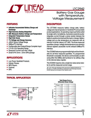
LTC2942Battery Gas Gaugewith Temperature,Voltage s Accumulated Battery Charge andDischargeHigh Accuracy Analog IntegrationADC Measures Battery Voltage and TemperatureIntegrated Temperature SensorHigh Side Sense1% Voltage and Charge Accuracy 50mV Sense Voltage RangeSMBus/I2C InterfaceConfigurable Alert Output/Charge Complete Input2.7V to 5.5V Operating RangeQuiescent Current Less than 100µASmall 6-Pin 2mm 3mm DFN packageApplicationsnnnnnLow Power Handheld ProductsCellular PhonesMP3 PlayersCamerasGPSThe LTC 2942 measures battery charge state, batteryvoltage and chip temperature in handheld PC and portableproduct applications. Its operating range is perfectly suitedfor single-cell Li-Ion batteries. A precision coulomb counterintegrates current through a sense resistor between thebattery’s positive terminal and the load or charger. Batteryvoltage and on-chip temperature are measured with aninternal 14-bit No Latency ADC. The three measuredquantities (charge, voltage and temperature) are stored ininternal registers accessible via the onboard SMBus/I2Cinterface.The LTC2942 features programmable high and low thresholds for all three measured quantities. If a programmedthreshold is exceeded, the device communicates an alertusing either the SMBus alert protocol or by setting a flagin the internal status register.The LTC2942 requires only a single low value sense resistor to set the measured current range.L, LT, LTC, LTM, Linear Technology and the Linear logo are registered trademarks andNo Latency Σ, ThinSOT and Bat-Track are trademarks of Linear Technology Corporation.All other trademarks are the property of their respective owners.Typical ApplicationTotal Charge Error vsDifferential Sense Voltage2.0LOAD0.1µFSENSE I2C/SMBusTO HOSTLTC2942AL/CCSDASENSE–SCLGNDRSENSE100mΩ 1-CELLLi-Ion2942 TA01aCHARGE ERROR (%)CHARGERVSENSE NSE (mV)2942 TA01b2942fa1
LTC2942Absolute Maximum Ratings(Notes 1, 2)Pin ConfigurationSupply Voltage (SENSE ). –0.3V to 6VSCL, SDA, AL/CC. –0.3V to 6VSENSE–. –0.3V to (VSENSE 0.3V)Operating Ambient Temperature RangeLTC2942C. 0 C to 70 CLTC2942I. –40 C to 85 CStorage Temperature Range. –65 C to 150 CTOP VIEW6 SENSE–SENSE 1GND 275 AL/CC4 SDASCL 3DCB PACKAGE6-LEAD (2mm 3mm) PLASTIC DFNTJMAX 150 C, θJA 120 C/WEXPOSED PAD (PIN 7), DO NOT CONNECTOrder InformationLead Free FinishTAPE AND REEL (MINI)TAPE AND REELPART MARKING*PACKAGE DESCRIPTIONTEMPERATURE RANGELTC2942CDCB#TRMPBFLTC2942CDCB#TRPBFLDVN6-Lead (2mm 3mm) Plastic DFN0 C to 70 CLTC2942IDCB#TRMPBFLTC2942IDCB#TRPBFLDVN6-Lead (2mm 3mm) Plastic DFNTRM 500 pieces. *Temperature grades are identified by a label on the shipping container.Consult LTC Marketing for parts specified with wider operating temperature ranges.Consult LTC Marketing for information on lead based finish parts.For more information on lead free part marking, go to: http://www.linear.com/leadfree/For more information on tape and reel specifications, go to: http://www.linear.com/tapeandreel/–40 C to 85 CElectrical CharacteristicsThe l denotes the specifications which apply over the full operatingtemperature range, otherwise specifications are at TA 25 C. (Note 2)SYMBOLPARAMETERCONDITIONSMINTYPMAXUNITSPower RequirementsVSENSE Supply VoltageISUPPLYSupply Current (Note 3)2.75.5Battery Gas Gauge On, ADC Sleep70100µABattery Gas Gauge On, ADC Converting Voltagel300350µABattery Gas Gauge On, ADC Converting Temperature l350420µA2.5µA1µA2.7V 50mVShutdownlShutdown, VSENSE 4.2VVUVLOUndervoltage Lockout ThresholdVlVSENSE FallinglVSENSE – VSENSE–l2.52.6Coulomb CounterVSENSESense Voltage Differential InputRangeRIDRDifferential Input Resistance,Across SENSE and SENSE–(Note 8)400kΩ2942fa2
LTC2942Electrical CharacteristicsThe l denotes the specifications which apply over the full operatingtemperature range, otherwise specifications are at TA 25 C. (Note 2)SYMBOLPARAMETERCONDITIONSqLSBCharge LSB (Note 4)Prescaler M 128 (Default), RSENSE 50mΩTCETotal Charge Error (Note 5)10mV VSENSE 50mV DCMINTYPMAX0.085UNITSmAh 1%10mV VSENSE 50mV DC, VSENSE 4.2Vl 1.5%1mV VSENSE 50mV DC (Note 8)l 3.5%(Note 8)lVoltage Measurement ADCResolution (No Missing Codes)VFSFull-Scale Voltage VLSBQuantization Step of 14-BitVoltage ADCTUEVVoltage Total Unadjusted Error14l(Note 6)Bits6V366.2µV11.3lGainGain AccuracyVOSOffsetINLIntegral NonlinearityltCONVConversion Timel1.3% 1 10LSB 1 4LSB15mslExtrapolated from Measurements at 5.5V and 2.7V%%Temperature Measurement ADCResolution (No Missing Code)(Note 8)TFSFull-Scale Temperature TLSBQuantization Step of 10-BitTemperature ADC(Note 6)TUETTemperature Total UnadjustedErrorVSENSE 2.8V (Note 8)tCONVConversion Time10lBits600K0.586Kl 5 3KKl15msDigital Inputs and Digital OutputsVITHLogic Input Threshold, AL/CC,SCL, SDAlVOLLow Level Output Voltage, AL/CC, I 3mASDAlIINInput Leakage, AL/CC, SCL, SDAVIN VSENSE /2CINInput Capacitance, AL/CC, SCL,SDA(Note 8)tPCCMinimum Charge Complete (CC)Pulse Width0.3 VSENSE 0.7 VSENSE V0.4Vl1µAl10pF1µsI2C Timing CharacteristicsfSCL(MAX)Maximum SCL Clock FrequencyltBUF(MIN)Bus Free Time Between STOP/STARTl1.3µstSU,STA(MIN) Minimum Repeated STARTSet-Up Timel600nstHD,STA(MIN) Minimum Hold Time (Repeated)START Conditionl600nstSU,STO(MIN) Minimum Set-Up Time for STOPConditionl600nstSU,DAT(MIN) Minimum Data Set-UpTime Inputl100nstHD,DATI(MIN) Minimum Data Hold Time Inputl0µs400900kHz2942fa3
LTC2942Electrical CharacteristicsThe l denotes the specifications which apply over the full operatingtemperature range, otherwise specifications are at TA 25 C. (Note 2)SYMBOLPARAMETERtHD,DATOData Hold Time OutputtOFData Output Fall TimeCONDITIONSMIN(Notes 7, 8)Note 1: Stresses beyond those listed under Absolute Maximum Ratingsmay cause permanent damage to the device. Exposure to any AbsoluteMaximum Rating condition for extended periods may affect devicereliability and lifetime.Note 2: All currents into pins are positive, all voltages are referenced toGND unless otherwise specifiedNote 3: ISUPPLY ISENSE ISENSE–Note 4: The equivalent charge of an LSB in the accumulated chargeregister depends on the value of RSENSE and the setting of the internalprescaling factor M:qLSB 0.085mAh TYPMAXUNITSl0.30.9µsl20 0.1 CB300nsNote 5: Deviation of qLSB from its nominal value.Note 6: The quantization step of the 14-bit ADC in voltage mode and10-bit ADC in temperature mode is not to be mistaken with the LSB of thecombined 16-bit voltage registers (I, J) and 16-bit temperature registers(M, N).Note 7: CB Capacitance of one bus line in pF (10pF CB 400pF). SeeVoltage and Temperature Registers section for more information.Note 8: Guaranteed by design, not subject to test.50mΩ M RSENSE 128See Choosing RSENSE and Choosing Coulomb Counter Prescaler M sectionfor more information. 1mAh 3.6C (coulombs).TIMING DIAGRAMtofSDAtSU, DATtHD, DATO,tHD, DATItSU, STAtHD, STAtBUFtSU, STO2942 F01SCLtHD, STASTARTCONDITIONREPEATED STARTCONDITIONSTOPCONDITIONSTARTCONDITIONFigure 1. Definition of Timing on I2C Bus2942fa4
LTC2942Typical Performance CharacteristicsTotal Charge Error vs DifferentialSense VoltageTotal Charge Errorvs Supply VoltageCHARGE ERROR �2–0.75VSENSE 2.7VVSENSE 4.2V–30.1110–1.001003.03.5VSENSE (mV)4.0 4.55.0VSENSE (V)5.52942 G016.03.54.0 4.55.0VSENSE (V)5.57510081.0TA 25 CTA –40 CTA 85 C506.002.53.03.54.0 4.55.0VSENSE (V)5.52942 G046.06TA 85 C420TA –45 C–2–4–6TA 25 C–8–102.53.03.54.0 4.55.0VSENSE– (V)2942 G05Voltage Measurement ADCIntegral Nonlinearity5.56.02942 G06Temperature Error vs Temperature1.03TA 85 C2TEMPERATURE ERROR ( C)3.025500TEMPERATURE ( C)100.5402.5–252942 G032.0ISHUTDOWN (µA)600.5INL (VLSB)ISUPPLY (µA)70–1.00–50VSENSE –50mVVSENSE –10mVVoltage Measurement ADCTotal Unadjusted Error1.580–0.50Shutdown Supply Currentvs Supply VoltageTA 25 CTA –40 CTA 85 C90–0.252942 G02Supply Current vs Supply Voltage1000–0.75VSENSE –50mVVSENSE –10mV2.50.25TOTAL UNADJUSTED ERROR (mV)CHARGE ERROR (%)2Total Charge Error vs Temperature1.00CHARGE ERROR (%)30TA –40 CTA 25 C–0.510–1–2–1.02.53.03.54.0 4.5 5.0VSENSE– (V)5.56.02942 G07–3–50–2502550TEMPERATURE ( C)751002942 G082942fa5
LTC2942Pin FunctionsSENSE (Pin 1): Positive Current Sense Input and PowerSupply. Connect to the load/charger side of the senseresistor. VSENSE operating range is 2.7V to 5.5V.GND (Pin 2): Device Ground. Connect directly to the negative battery terminal.SCL (Pin 3): Serial Bus Clock Input.SDA (Pin 4): Serial Bus Data Input and Output.AL/CC (Pin 5): Alert Output or Charge Complete Input.Configured either as an SMBus alert output or chargecomplete input by control register bits B[2:1]. At power-up,the pin defaults to alert mode conforming to the SMBusalert response protocol. It behaves as an open-drain logicoutput that pulls to GND when any threshold register valueis exceeded. When configured as a charge complete input,connect to the charge complete output from the batterycharger circuit. A high level at CC sets the value of theaccumulated charge (registers C, D) to FFFFh.SENSE– (Pin 6): Negative Current Sense Input. ConnectSENSE– to the positive battery terminal side of the senseresistor. The voltage between SENSE– and SENSE mustremain within 50mV in normal operation. SENSE– is alsothe input for the ADC in voltage measurement mode.Exposed Pad (Pin 7): Do Not Connect.Block Diagram1SENSE LTC2942VSUPPLYCOULOMB ENCEGENERATOROSCILLATORREF DAADC534DATA ANDCONTROLREGISTERSREF–GND2942 BD2942fa6
LTC2942OperationOverviewThe LTC2942 is a battery gas gauge device designed foruse with single Li-Ion cells and other battery types with aterminal voltage at 2.7V to 5.5V. It measures battery chargeand discharge, battery voltage and chip temperature.A precision coulomb counter integrates current through asense resistor between the battery’s positive terminal andthe load or charger. Battery voltage and on-chip temperatureare measured with an internal 14-bit/10-bit ADC.Coulomb CounterCharge is the time integral of current. The LTC2942 measures battery current by monitoring the voltage developedacross a sense resistor and then integrates this informationto infer charge. The differential voltage between SENSE and SENSE– is applied to an auto-zeroed differential analogintegrator to convert the measured current to charge.When the integrator output ramps to REFHI or REFLOlevels, switches S1, S2, S3 and S4 toggle to reverse theramp direction. By observing the condition of the switchesand the ramp direction, polarity is determined.CHARGERLOAD1SENSE BATTERYThe LTC2942 includes a 14-bit No Latency Σ analog-todigital converter, with internal clock and voltage referencecircuits.The ADC can either be used to monitor the battery voltageat SENSE– or to convert the output of the on-chip temperature sensor. The sensor generates a voltage proportional totemperature with a slope of 2.5mV/K resulting in a voltageof 750mV at 27 C.Conversion of either temperature or voltage is triggeredby setting the control register via the I2C interface. TheLTC2942 features an automatic mode where a voltage anda temperature conversion are executed every two seconds.At the end of each conversion the corresponding registersare updated and the converter goes to sleep to minimizequiescent current.REFHIVCCS1S36 Voltage and Temperature ADC– CONTROLLOGIC–S2RSENSEIBATA programmable prescaler effectively increases integrationtime by a factor M programmable from 1 to 128. At eachunderflow or overflow of the prescaler, the accumulatedcharge register (ACR) value is incremented or decrementedone count. The value of accumulated charge is read viathe I2C interface.2SENSE–MPRESCALER S4GNDACRREFLO–POLARITYDETECTION2942 F02Figure 2. Coulomb Counter Section of the LTC29422942fa7
LTC2942OperationPower-Up SequenceWhen SENSE rises above a threshold of approximately2.5V, the LTC2942 generates an internal power-on reset(POR) signal and sets all registers to their default state.In the default state, the coulomb counter is active whilethe voltage and temperature ADC is switched off. Theaccumulated charge register is set to mid-scale (7FFFh),all low threshold registers are set to 0000h and all highthreshold registers are set to FFFFh. The alert mode isenabled and the coulomb counter prescaling factor M isset to 128.Applications InformationI2C/SMBus InterfaceThe LTC2942 communicates with a bus master using a2-wire interface compatible with I2C and SMBus. The 7-bithard-coded I2C address of the LTC2942 is 1100100.The LTC2942 is a slave-only device. Therefore the serialclock line (SCL) is an input only while the serial data line(SDA) is bidirectional. The device supports I2C standardand fast mode. For more details refer to the I2C Protocolsection.Internal RegistersThe LTC2942 integrates current through a sense resistor,measures battery voltage and temperature and stores theresults in internal 16-bit registers accessible via I2C. Highand low limits can be programmed for each measurementquantity. The LTC2942 continuously monitors these limitsand sets a flag in the onboard status register when a limitis exceeded. If the alert mode is enabled, the AL/CC pinpulls low.The sixteen internal registers are organized as shown inTable 1.Table 1. Register MapADDRESSNAME REGISTER DESCRIPTIONR/WDEFAULT00hAStatusRSee Below01hBControlR/W3Ch02hCAccumulated Charge MSBR/W7Fh03hDAccumulated Charge LSBR/WFFh04hECharge Threshold High MSBR/WFFh05hFCharge Threshold High LSBR/WFFh06hGCharge Threshold Low MSBR/W00h07hHCharge Threshold Low LSBR/W00h08hIVoltage MSBRXXh09hJVoltage LSBRXXh0AhKVoltage Threshold HighR/WFFh0BhLVoltage Threshold LowR/W00h0ChMTemperature MSBRXXh0DhNTemperature LSBRXXh0EhOTemperature Threshold HighR/WFFh0FhPTemperature Threshold LowR/W00hR Read, W Write, XX Unknown2942fa8
LTC2942Applications InformationStatus Register (A)The status of the charge, voltage and temperature alertsis reported in the status register shown in Table 2.Table 2. Status Register A (Read only)BITNAMEA[7] Chip IdentificationOPERATIONDEFAULT0: LTC29421: LTC29410A[6] Reserved0A[5] Accumulated Charge Indicates that the value of theOverflow/Underflow ACR hit either top or bottom.0A[4] Temperature AlertIndicates one of thetemperature limits wasexceeded.0A[3] Charge Alert HighIndicates that the ACR valueexceeded the charge thresholdhigh limit.0A[2] Charge Alert LowIndicates that the ACR valuedropped below the chargethreshold low limit.0A[1] Voltage AlertIndicates one of the batteryvoltage limits was exceeded.0A[0] UndervoltageLockout AlertIndicates recovery fromundervoltage. If set to 1, aUVLO has occurred and thecontents of the registers areuncertain.XAll status register bits except A[7] are cleared after beingread by the host, if the conditions which set these bitshave been removed.As soon as one of the three measured quantities exceedsthe programmed limits, the corresponding bit A[4], A[3],A[2] or A[1] in the status register is set.Bit A[5] is set if the LTC2942’s accumulated charge registers(ACR) overflows or underflows. In these cases, the ACRstays at FFFFh or 0000h and does not roll over.The undervoltage lockout (UVLO) bit of the status registerA[0] is set if, during operation, the voltage on SENSE pin drops below 2.7V without reaching the POR level.The analog parts of the coulomb counter are switched offwhile the digital register values are retained. After recovery of the supply voltage the coulomb counter resumesintegrating with the stored value in the accumulatedcharge registers but it has missed any charge flowingwhile SENSE 2.7V.The hard-coded bit A[7] of the status register enables thehost to distinguish the LTC2942 from the pin compatibleLTC2941, allowing the same software to be used withboth devices.Control Register (B)The operation of the LTC2942 is controlled by programming the control register. Table 3 shows the organizationof the 8-bit control register B[7:0].Table 3. Control Register BBITNAMEOPERATIONDefaultB[7:6] ADC Mode[11] Automatic Mode.Performs voltage and temperatureconversion every second.[10] Manual Voltage Mode.Performs single voltageconversion, then sleeps.[01] Manual Temperature Mode.Performs single temperatureconversion, then sleeps.[00] Sleep.[00]B[5:3] Prescaler MSets coulomb counter prescalingfactor M between 1 and 128.Default is 128.M 2(4 B[5] 2 B[4] B[3])[111]B[2:1] AL/CC Configure Configures the AL/CC pin.[10] Alert Mode.Alert functionality enabled.Pin becomes logic output.[01] Charge Complete Mode.Pin becomes logic input andaccepts “charge complete” signal(e.g., from a charger) to setaccumulated charge register (C, D)to FFFFh.[00] AL/CC pin disabled.[11] Not allowed.B[0]ShutdownShut down analog section toreduce ISUPPLY.[10][0]Power Down B[0]Setting B[0] to 1 shuts down the analog parts of theLTC2942, reducing the current consumption to less than1µA. All analog circuits are inoperative while the valuesin the registers are retained. Note that any charge flowingwhile B[0] is 1 is not measured and the charge informationbelow 1LSB of the accumulated charge register is lost.2942fa9
LTC2942Applications InformationAlert/Charge Complete Configuration B[2:1]The AL/CC pin is a dual function pin configured by thecontrol register. By setting bits B[2:1] to [10] (default)the AL/CC pin is configured as an alert pin following theSMBus protocol. In this configuration the AL/CC pin is adigital output and is pulled low if one of the three measured quantities (charge, voltage, temperature) exceedsits high or low threshold or if the value of the accumulatedcharge register overflows or underflows. An alert responseprocedure started by the master resets the alert at theAL/CC pin. For further information see the Alert ResponseProtocol section.Setting the control bits B[2:1] to [01] configures the AL/CCpin as a digital input. In this mode, a high input on theAL/CC pin communicates to the LTC2942 that the batteryis full and the accumulated charge register is set to itsmaximum value FFFFh. The AL/CC pin would typicallybe connected to the “charge complete” output from thebattery charger circuitry.If neither the alert nor the charge complete functionalityis desired, bits B[2:1] should be set to [00]. The AL/CCpin is then disabled and should be tied to GND.Avoid setting B[2:1] to [11] as it enables the alert and thecharge complete modes simultaneously.Choosing RSENSETo achieve the specified precision of the coulomb counter,the differential voltage between SENSE and SENSE– muststay within 50mV. For differential input signals up to 300mV the LTC2942 will remain functional but the precision of the coulomb counter is not guaranteed.The required value of the external sense resistor, RSENSE,is determined by the maximum input range of VSENSE andthe maximum current of the application:RSENSE 50mVIMAXThe choice of the external sense resistor value influencesthe gain of the coulomb counter. A larger sense resistorgives a larger differential voltage between SENSE andSENSE– for the same current which results in more precisecoulomb counting. Thus the amount of charge representedby the least significant bit (qLSB) of the accumulated charge(registers C, D) is equal to:qLSB 0.085mAh 50mΩ M RSENSE 128qLSB 0.085mAh 50mΩRSENSEorwhen the prescaler is set to its default value of M 128.Note that 1mAh 3.6C (coulomb).Choosing RSENSE 50mV/IMAX is not sufficient in applications where the battery capacity (QBAT) is very largecompared to the maximum current (IMAX):QBAT IMAX 5.5 HoursFor such low current applications with a large battery,choosing RSENSE according to RSENSE 50mV/IMAX canlead to a qLSB smaller than QBAT/216 and the 16-bit accumulated charge register may underflow before the batteryis exhausted or overflow during charge. Choose, in thiscase, a maximum RSENSE of:RSENSE 0.085mAh 216 50mΩQBATIn an example application where the maximum current isIMAX 100mA, calculating RSENSE 50mV/IMAX wouldlead to a sense resistor of 500mΩ. This gives a qLSB of8.5µAh and the accumulated charge register can representa maximum battery capacity of QBAT 8.5µAh 65535 557mAh. If the battery capacity is larger, RSENSE must belowered. For example, RSENSE must be reduced to 150mΩif a battery with a capacity of 1800mAh is used.2942fa10
LTC2942Applications InformationChoosing Coulomb Counter Prescaler M B[5:3]If the battery capacity (QBAT) is very small compared tothe maximum current (IMAX) (QBAT IMAX 0.1 Hours)the prescaler value M should be changed from its defaultvalue (128).In these applications with a small battery but a highmaximum current, qLSB can get quite large with respectto the battery capacity. For example, if the battery capacityis 100mAh and the maximum current is 1A, the standardequation leads to choosing a sense resistor value of50mΩ, resulting in:qLSB 0.085mAh 306mCThe battery capacity then corresponds to only 1176 qLSBsand less than 2% of the accumulated charge register isutilized.To preserve digital resolution in this case, the LTC2942includes a programmable prescaler. Lowering the prescaler factor M allows reducing qLSB to better match theaccumulated charge register to the capacity of the battery.The prescaling factor M can be chosen between 1 and itsdefault value 128. The charge LSB then becomes:qLSB 0.085mAh 50mΩ M RSENSE 128Note that the internal digital resolution of the coulombcounter is higher than indicated by qLSB. The digitizedcharge qINTERNAL is M 8 times smaller than qLSB. qINTERNALis typically 299µAs for a 50mΩ sense resistor.ADC Mode B[7:6]The LTC2942 features an ADC which measures eithervoltage on SENSE– (battery voltage) or temperature viaan internal temperature sensor. The reference voltage andclock for the ADC are generated internally.The ADC has four different modes of operation, as shownin Table 3. These modes are controlled by bits B[7:6] ofthe control register. At power-up, bits B[7:6] are set to[00] and the ADC is in sleep mode.A single voltage conversion is initiated by setting the bitsB[7:6] to [10]. A single temperature conversion is startedby setting bits B[7:6] to [01]. After a single voltage ortemperature conversion, the ADC resets B[7:6] to [00]and goes to sleep.The LTC2942 also offers an automatic scan mode wherethe ADC converts voltage, then temperature, then sleepsfor approximately two seconds before repeating the voltageand temperature conversions. The LTC2942 is set to thisautomatic mode by setting B[7:6] to [11] and stays in thismode until B[7:6] are reprogrammed by the host.To use as much of the range of the accumulated chargeregister as possible the prescaler factor M should bechosen for a given battery capacity QBAT and a senseresistor RSENSE as:Programming B[7:6] to [00] puts the ADC to sleep. Ifcontrol bits B[7:6] change within a conversion, the ADCwill complete the current conversion before entering thenewly selected mode.RSENSE 0.085mAh 50mΩM can be set to 1, 2, 4, 8, 128 by programming B[5:3] ofthe control register as M 2(4 B[5] 2 B[4] B[3]). The defaultvalue after power up is M 128 27 (B[5:3] 111).A conversion of either voltage or temperature requires 10msconversion time (typical). At the end of each conversion,the corresponding registers are updated. If the convertedquantity exceeds the values programmed in the thresholdregisters, a flag is set in the status register and the AL/CCpin is pulled low (if alert mode is enabled).In the above example of a 100mAh battery and an RSENSEof 50mΩ, the prescaler should be programmed to M 4.The qLSB then becomes 2.656µAh and the battery capacitycorresponds to roughly 37650 qLSBs.During a voltage conversion, the SENSE– pin is connectedthrough a small resistor to a sampling circuit with anequivalent resistance of 2MΩ, leading to a mean inputcurrent of I VSENSE–/2MΩ.M 128 162QBAT 2942fa11
LTC2942Applications InformationAccumulated Charge Register (C, D)The coulomb counter of the LTC2942 integrates currentthrough the sense resistor. The result of this charge integration is stored in the 16-bit accumulated charge register(registers C, D). As the LTC2942 does not know the actualbattery status at power-up, the accumulated charge register(ACR) is set to mid-scale (7FFFh). If the host knows thestatus of the battery, the accumulated charge (C[7:0]D[7:0])can be either programmed to the correct value via I2C orit can be set after charging to FFFFh (full) by pulling theAL/CC pin high if charge complete mode is enabled viabits B[2:1]. Before writing the accumulated charge registers, the analog section should be shut down by settingB[0] to 1. In order to avoid a change in the accumulatedcharge registers between reading MSBs C[7:0] and LSBsD[7:0], it is recommended to read them sequentially, asshown in Figure 10.Voltage and Temperature Registers (I, J), (M, N)The result of the 14-bit ADC conversion of the voltage atSENSE– is stored in the voltage registers (I, J), whereasthe temperature measurement result is stored in the temperature registers (M, N). The voltage and temperatureregisters are read only.As the ADC resolution is 14-bit in voltage mode and 10-bitin temperature mode, the lowest two bits of the combinedvoltage registers (I, J) and the lowest six bits of thecombined temperature registers (M, N) are always zero.From the result of the 16-bit voltage registers I[7:0]J[7:0]the measured voltage can be calculated as:VSENSE – 6V RESULTDECRESULTh 6V FFFFh65535Example: a register value of I[7:0] B0h and J[7:0] 1Chcorresponds to a voltage on SENSE– of:45084DECB01ChVSENSE – 6 V 6V 4.12776V65535FFFFhThe actual temperature can be obtained from the two byteregister C[7:0]D[7:0] by:T 600K RESULTDECRESULTh 600K FFFFh65535Example: a register value of C[7:0] 80h D[7:0] 00hcorresponds to 300K or 27 C.Threshold Registers (E, F, G, H, K, L, O, P)For each of the measured quantities (battery charge, voltage and temperature) the LTC2942 features a high and alow threshold registers. At power-up, the high thresholdsare set to FFFFh while the low thresholds are set to 0000h.All thresholds can be programmed to a desired value viaI2C. As soon as a measured quantity exceeds the highthreshold or falls below the low threshold, the LTC2942sets the corresponding flag in the status register andpulls the AL/CC pin low if alert mode is enabled via bitsB[2:1]. Note that the voltage and temperature thresholdregisters are single-byte registers and only the 8 MSBs ofthe corresponding quantity are checked. To set a low levelthreshold for the battery voltage of 3V, register L shouldbe programmed to 80h; a high temperature limit of 60 Cis programmed by setting register O to 8Eh.I2C ProtocolThe LTC2942 uses an I2C/SMBus compatible 2-wire opendrain interface supporting multiple devices and masterson a single bus. The connected devices can only pull thebus wires LOW and they never drive the bus HIGH. Thebus wires must be externally connected to a positive supply voltage via a current source or pull-up resistor. Whenthe bus is idle, both SDA and SCL are HIGH. Data on theI2C bus can be transferred at rates of up to 100kbit/s instandard mode and up to 400kbit/s in fast mode.Each device on the I2C/SMBus is recognized by a uniqueaddress stored in that device and can operate as either atransmitter or receiver, depending on the function of thedevice. In addition to transmitters and receivers, devicescan also be classified as masters or slaves when performing data transfers. A master is the device which initiates adata transfer on the bus and generates the clock signalsto permit that transfer. At the same time any device ad2942fa12
LTC2942Applications Informationdressed is considered a slave. The LTC2942 always actsas a slave.Figure 3 shows an overview of the data transmission forfast and standard mode on the I2C bus.START and STOP ConditionsWhen the bus is idle, both SCL and SDA must be HIGH. Abus master signals the beginning of a transmission with aSTART condition by transitioning SDA from HIGH to LOWwhile SCL is HIGH. When the master has finished communicating with the slave, it issues a STOP condition bytransitioning SDA from LOW to HIGH while SCL is HIGH.The bus is then free for another transmission. Whenthe bus is in use, it stays busy if a repeated START (Sr)is generated instead of a STOP condition. The repeatedSTART (Sr) conditions are functionally identical to theSTART (S).Data TransmissionAfter a START condition, the I2C bus is considered busyand data transfer begins between a master and a slave.As data is transferred over I2C in groups of nine bits(eight data bits followed by an acknowledge bit), eachSDAa6 - a0SCL1-789ADDRESSR/WACKgroup takes nine SCL cycles. The transmitter releasesthe SDA line during the acknowledge clock pulse and thereceiver issues an acknowledge (ACK) by pulling SDALOW or leaves SDA HIGH to indicate a not acknowledge(NACK) condition. Change of data state can only happenwhile SCL is LOW.Write ProtocolThe master begins a write operation with a START condition followed by the seven bit slave address 1100100and the R/W bit set to zero, as shown in Figure 4. TheLTC2942 acknowledges this by pulling SDA LOW andthen the master sends a command byte which indicateswhich internal register the master is to write. The LTC2942acknowledges and latches the command byte into itsinternal register address pointer. The master delivers thedata byte, the LTC2942 acknowledges once more andlatches the data into the desired register. The transmissionis ended when the master sends a STOP condition. If themaster continue
voltage and chip temperature in handheld PC and portable product applications. Its operating range is perfectly suited for single-cell Li-Ion batteries. A precision coulomb counter integrates current through a sense resistor between the battery's positive terminal and the load or charger. Battery voltage and on-chip temperature are measured .


![Smarter Battery Crack [2022-Latest]](/img/13/eliamari.jpg)