Transcription
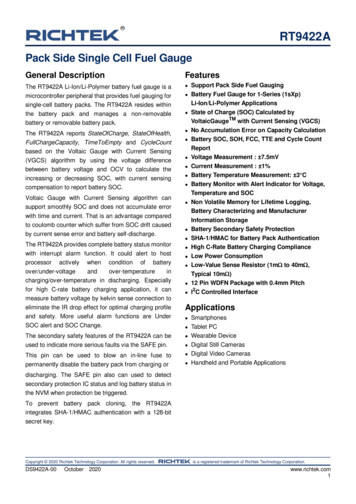
RT9422APack Side Single Cell Fuel GaugeGeneral DescriptionFeaturesThe RT9422A Li-Ion/Li-Polymer battery fuel gauge is amicrocontroller peripheral that provides fuel gauging forsingle-cell battery packs. The RT9422A resides withinthe battery pack and manages a non-removablebattery or removable battery pack. The RT9422A reports StateOfCharge, StateOfHealth,FullChargeCapacity, TimeToEmpty and CycleCountbased on the Voltaic Gauge with Current Sensing(VGCS) algorithm by using the voltage differencebetween battery voltage and OCV to calculate theincreasing or decreasing SOC, with current sensingcompensation to report battery SOC.Voltaic Gauge with Current Sensing algorithm cansupport smoothly SOC and does not accumulate errorwith time and current. That is an advantage comparedto coulomb counter which suffer from SOC drift causedby current sense error and battery self-discharge.The RT9422A provides complete battery status monitorwith interrupt alarm function. It could alert to hostprocessor actively when condition of ging/over-temperature in discharging. Especiallyfor high C-rate battery charging application, it canmeasure battery voltage by kelvin sense connection toeliminate the IR drop effect for optimal charging profileand safety. More useful alarm functions are UnderSOC alert and SOC Change. Support Pack Side Fuel GaugingBattery Fuel Gauge for 1-Series (1sXp)Li-Ion/Li-Polymer ApplicationsState of Charge (SOC) Calculated byVoltaicGaugeTM with Current Sensing (VGCS)No Accumulation Error on Capacity CalculationBattery SOC, SOH, FCC, TTE and Cycle CountReportVoltage Measurement : 7.5mVCurrent Measurement : 1%Battery Temperature Measurement: 3 CBattery Monitor with Alert Indicator for Voltage,Temperature and SOCNon Volatile Memory for Lifetime Logging,Battery Characterizing and Manufacturer Information StorageBattery Secondary Safety ProtectionSHA-1/HMAC for Battery Pack AuthenticationHigh C-Rate Battery Charging ComplianceLow Power ConsumptionLow-Value Sense Resistor (1m to 40m ,Typical 10m )12 Pin WDFN Package with 0.4mm Pitch I2C Controlled Interface ApplicationsThe secondary safety features of the RT9422A can be used to indicate more serious faults via the SAFE pin. This pin can be used to blow an in-line fuse to SmartphonesTablet PCWearable DeviceDigital Still CamerasDigital Video Cameraspermanently disable the battery pack from charging or Handheld and Portable Applications discharging. The SAFE pin also can used to detectsecondary protection IC status and log battery status inthe NVM when protection be triggered.To prevent battery pack cloning, the RT9422Aintegrates SHA-1/HMAC authentication with a 128-bitsecret key.Copyright 2020 Richtek Technology Corporation. All rights reserved.DS9422A-00October2020is a registered trademark of Richtek Technology Corporation.www.richtek.com1
RT9422AOrdering InformationPin Configuration(TOP VIEW)RT9422APackage TypeQW : WDFN-12L 2.5x4 (W-Type)SAFEVBATGVDDVBATSVPTSVSSLead Plating SystemG : Green (Halogen Free and Pb Free)Note :123456GND13121110987ALERTSCLSDATSCSNCSPWDFN-12L 2.5x4Richtek products are : Marking InformationRoHS compliant and compatible with the currentrequirements of IPC/JEDEC J-STD-020. 03 : Product CodeW : Date CodeSuitable for use in SnPb or Pb-free soldering03Wprocesses.Simplified Application CircuitSingle-Cell Li-ion / Li-PolymerBattery PackHost SystemPACK ight 2020 Richtek Technology Corporation. All rights reserved.www.richtek.com2PACK-is a registered trademark of Richtek Technology Corporation.DS9422A-00October2020
RT9422AFunctional Pin DescriptionPin No.Pin NamePin Function1SAFEOutput mode to enforce secondary safety protection; Input mode to detectoutput status of secondary protection IC.2VBATGBattery voltage sensing negative input. Connect to battery connector withkelvin connection.3VDD4VBATSBattery voltage sensing positive input. Connect to battery connector withkelvin connection.5VPTSPower reference output pin for temperature measurement.6VSSDevice ground.7CSPBattery current sensing positive input. Connect a 10m sense resistor withkelvin connection where is near BAT- side.8CSNBattery current sensing negative input. Connect a 10m sense resistor withkelvin connection where is near PACK- side.9TS10SDASerial data input. Slave I2C serial communications data line forcommunication with system. Open-drain I/O.11SCLSerial cock input. Slave I2C serial communications clock line forcommunication with system. Open-drain I/O.12ALERTPower supply input.Temperature measurement input.Option for alert open-drain indicator output or single wire communicationpin.Functional Block DiagramVDDVREFVPTSALERTVGCS EngineCommunicationSDASCLTSVoltaic GaugeTMVBATSControllerSAFEADCVBATGCurrent SensingCompensationCSPNVMCSNVSSCopyright 2020 Richtek Technology Corporation. All rights reserved.DS9422A-00October2020is a registered trademark of Richtek Technology Corporation.www.richtek.com3
RT9422AAbsolute Maximum Ratings(Note 1) Voltage on CSN Pin to CSP ------------------------------ 0.3V to 2V Voltage on VBATS, VBATG, VPTS, TS to VSS ----- 0.3V to (VDD 0.3V) Voltage on VDD Pin Relative to VSS ------------------- 0.3V to 6V Voltage on All Other Pins Relative to VSS ------------ 0.3V to 6V Power Dissipation, PD @ TA 25 CWDFN-12L 2.5x4 -------------------------------------------- 3.25W Package Thermal Resistance(Note 2)WDFN-12L 2.5x4, JA -------------------------------------- 30.7 C/WWDFN-12L 2.5x4, JC -------------------------------------- 4 C/W Lead Temperature (Soldering, 10 sec.) ---------------- 260 C Junction Temperature -------------------------------------- 150 C Storage Temperature Range ----------------------------- 65 C to 150 C ESD Susceptibility(Note 3)HBM (Human Body Model) ------------------------------- 2kVRecommended Operating Conditions(Note 4) Supply Voltage, VDD -------------------------------------- 2.5V to 5.5V Ambient Temperature --------------------------------- 40 C to 85 C Junction Temperature Range --------------------------- 40 C to 125 CElectrical Characteristics(2.5V VDD 5.5V, TA 25 C, unless otherwise specified)ParameterSymbolOperation VoltageTest ConditionsVDD - VSSMinTypMaxUnit2.5--5.5VActive CurrentIACTIVEActive mode, VDD 3.8V--1420 ASleep CurrentISLEEPSleep mode, VDD 3.8V--57 AShutdown CurrentISHUTDOWNVDD 3.8V--0.51 A2.5--VDDVVBATS 4V, VBATG 0V 7.5--7.5mVVCSP - VCSN 125--125mVVoltage Measurement RangeVoltage Measurement ErrorVERRCurrent Measurement RangeCurrent Measurement GainErrorIGERR VCSP-VCSN 20mV 1--1%Current Measurement OffsetErrorIOERR VCSP-VCSN 0V (Note 5) 10 510 VTemperature MeasurementErrorExtTGERRTA 25 C 3--3 C 40--85 C-- 3-- CInternal TemperatureMeasurement RangeInternal TemperatureMeasurement Error(Note 7)IntTGERRTA 25 CCopyright 2020 Richtek Technology Corporation. All rights reserved.www.richtek.com4(Note 6)is a registered trademark of Richtek Technology Corporation.DS9422A-00October2020
RT9422AParameterSymbolMinTypMaxUnitInput Impedance :VBATS, VBATG, TS15----M Input Impedance :CSN, CSP1----M 1.1461.21.254VVPTS Output DriveTest ConditionsIOUT 0.5mAInput Logic-High :SCL, SDA, ALERTVIHReference to VSS1.4----VInput Logic-High : SAFEVIHReference to VSS0.7xVDD----VInput Logic-Low :SCL, SDA, ALERTVILReference to VSS----0.5VInput Logic-Low : SAFEVILReference to VSS----0.3xVDDVOutput Logic-High : SAFEVOHIOH 3mA (Reference to VSS)VDD 0.4V----VOutput Logic-Low :SDA, ALERT, SAFEVOLIOL 3mA (Reference to VSS)----0.4VPulldown Current :SCL, SDA, ALERTIPDNVDD 4.5V, VSCL,0.4V0.050.20.4 ANVM Read CurrentIREAD----4mANVM Write CurrentIWRITE----7mANVM Read TimetREAD----2msNVM Write 400kHz1.3---- s0.6---- sLow Period of the SCL Clock tLOW1.3---- sHigh Period of the SCLClocktHIGH0.6---- sSetup Time for a RepeatedSTART ConditiontSU:STA0.6---- sData Hold TimetHD:DAT(Note 9, 10)0--0.9 sData Setup TimetSU:DAT(Note 9)100----nsClock Data Rise TimetR20--300nsSDA, ALERTNVM Endurance Electrical Characteristics : I2C Interface(2.5V VDD 4.5V, TA 25 C, unless otherwise specified)ParameterSymbolClock Operating Frequencyf SCLTest Conditions(Note 8)Bus Free Time Between atBUFSTOP and START ConditionHold Time After STARTConditiontHD:STA(Note 8)Copyright 2020 Richtek Technology Corporation. All rights reserved.DS9422A-00October2020is a registered trademark of Richtek Technology Corporation.www.richtek.com5
RT9422AParameterSymbolTest ConditionsMinTypMaxUnit0--300ns0.6---- sClock Data Fall TimetFSet-Up Time for STOPConditiontSU:STOSpike Pulse WidthsSuppressed by Input FiltertSP(Note 11)0--50nsCapacitive Load for EachBus LineCB(Note 12)----400pFSCL, SDA InputCapacitanceCBIN----60pFNote 1. Stresses beyond those listed under “Absolute Maximum Ratings” may cause permanent damage to the device. Theseare stress ratings only, and functional operation of the device at these or any other conditions beyond those indicated inthe operational sections of the specifications is not implied. Exposure to absolute maximum rating conditions may affectdevice reliability.Note 2. JA is measured under natural convection (still air) at TA 25 C with the component mounted on a higheffective-thermal-conductivity four-layer test board on a JEDEC 51-7 thermal measurement standard. JC is measuredat the top of the package.Note 3. Devices are ESD sensitive. Handling precaution is recommended.Note 4. The device is not guaranteed to function outside its operating conditions.Note 5. Typical result is long time average.Note 6. The thermistor is use 10k NTC and beta 3435k, default is SEMITEC 103KT1608T.Note 7. Specifications are 100% tested at TA 25 C. Limits over the operating range are guaranteed by design andcharacterization.Note 8. fSCL must meet the minimum clock low time plus the rise/fall times.Note 9. The maximum tHD:DAT has only to be met if the device does not stretch the low period (t LOW ) of the SCL signal.Note 10. This device internally provides a hold time of at least 75ns for the SDA signal (referred to the V IHMIN) of the SCL signal)to bridge the undefined region of the falling edge of SCL.Note 11. Filters on SDA and SCL suppress noise spikes at the input buffers and delay the sampling instant.Note 12. CB – total capacitance of one bus line in pF.Copyright 2020 Richtek Technology Corporation. All rights reserved.www.richtek.com6is a registered trademark of Richtek Technology Corporation.DS9422A-00October2020
RT9422ATypical Application CircuitFUSEC20.1µFPACK NMOSM13VDD4C7SAFE 0.1µF1RT9422AALERT5 10kΩ(optional)78Copyright 2020 Richtek Technology Corporation. All rights reserved.2020R6100Ω10R7100ΩR10 atteryProtectionModulePACK-is a registered trademark of Richtek Technology Corporation.www.richtek.com7
RT9422ATypical Operating Characteristics* : Sample accuracy with custom parameter into the IC.Voltage ADC Error vs. TemperatureCurrent ADC Error vs. Temperature1010 40 C86Current ADC Error (mA)85 C42025 C-2-4-6-8 40 C64285 C025 C-2-4-6-8-10-2000 -1500 -1000 0500 1000 1500 2000Current (mA)Voltage (mV)Temperature Measurement Error vs. TemperatureSOC Accuracy*51004903802701SOC (%)Temperature Measurement Error ( C)100-1-2SOC VGCSReference SOCSOC Error VGCS-3-44C/4 DCHG602500C/4 CHG40-2C/2 CHG20-4-61.5C CHGC/2 DCHG10-5-80-40-20020254565Temperature ( C)Copyright 2020 Richtek Technology Corporation. All rights reserved.www.richtek.com88630VDD 2.5VVDD 3.5VVDD 4.5V10SOC Error (%)Voltage ADC Error (mV)885-10012345678910Time (h)is a registered trademark of Richtek Technology Corporation.DS9422A-00October2020
RT9422AApplication InformationThe RT9422A reports temperature to Temperatureregister by measuring battery temperature or chipADC for Voltage, Current and TemperatureBattery voltage is measured at the VBATS pin inputwith respect to VBATG over a 2.5 to 5.5V range withresolutions of 1mV. The ADC calculates the first cellvoltage for a period of 250ms after IC POR and then fora period of 1s for every cycle afterwards. The Voltagetemperature. When measuring battery temperature, anexternal NTC resistor will be used.register requires 1s to update after exiting Sleep mode.The result is placed in the Voltage register at the end ofeach conversion period.The VGCS algorithm is based on the battery voltageand the dynamic difference of battery voltage andbattery current measurement, by iterating batteryvoltage information and compensating with currentinformation to increase or decrease delta SOC, thenThe RT9422A Fuel Gauge measures battery current incharging and discharging and reports it to Currentregister. The measurement range is 10A (RS 10m ),and the resolution is 1mA.InputVoltaicGauge with Current Sensing (VGCS)Algorithmintegrate to SOC. The below figure is for VGCSfunctional block.VGCS AlgorithmOCV Table taicGaugewith Current ureBattery CapacityCompensationTimetoEmptyDesignCapacityThe RT9422A got battery voltage information thenusing OCV table and iterate calculation with currentcorrection to calculate delta SOC, then using designcapacity and battery capacity as a reference tooptimize result and output final SOC result. VGCS alsosupport high C-RATE charging technology.The coulomb counter based fuel gauge suffers fromSOC drift due to current-sense error and cellself-discharge. Even there is a very small currentsensing error, the coulomb counter accumulates theerror from time to time, VGCS is based on voltageiteration algorithm to reach stable SOC behavior andonly using current information to fine tune result forgetting good transient state response. VGCS does notaccumulate current and suffer SOC drift issue liketraditional coulomb counter.Copyright 2020 Richtek Technology Corporation. All rights reserved.DS9422A-00October2020Design CapacityThe DesignCapacity register should be set with propervalue after IC POR, Design Capacity is the expectedcapacity when cell has been made and it’s not beenchanged when VGCS active. Design Capacity is usedas a reference input for VGCS algorithm. Theresolution of Design Capacity is 1mAh and defaultvalue is 0x079E (1950mAh).SOC ReportThe StateOfCharge register is a read-only register thatdisplays the state of charge of the cell as calculated bythe VGCS algorithm. The result is displayed as apercentage of the cell’s full capacity. This registerautomatically adapts to variation in battery size sincethe Fuel Gauge naturally recognize relative SOC. Theis a registered trademark of Richtek Technology Corporation.www.richtek.com9
RT9422Aunits of SOC is %. The reported SOC also includesresidual capacity, which might not be available to theactual application because of early termination voltagePower Mode SwitchingPORrequirements. When SOC 0, typical applications haveno remaining capacity. The first update occurs in250ms after POR of the IC.Power ModeThere are three power mode for the RT9422A. Eachpower mode could be applied on different applicationfor different power consumption considering. The threepower modes are Active mode, Sleep mode andShutdown mode.Active ModeThe active mode is recommended and it is the defaultpower mode after POR. In active mode, the Current and AverageTemperature will beupdated every second.Sleep ModeThe sleep mode behavior is same as the active modebut it has the longer measurement period. The period inthe sleep mode is programmable. The minimum periodis 2 times of active mode and the maximum period is 16times of active mode. The default period is 4 times ofactive mode. When sleep mode function is enabled, itcould be entered/exited by sending commands or byFuel Gauge self-detection.Shutdown ModeActive1. Exit shutdown command22. I C pull highDisable Sleep Mode or1. Exit sleep command or2. FG self-detected exitEnable Shutdown Mode &1. Entry shutdown command or22. SHDN LOW EN 1 & I C pull lowShutdownEnable Sleep Mode &1. Entry sleep command or2. FG self-detected entrySleep1. Exit shutdown command22. I C pull high*: Exit sleep mode command is available for FG self-detected entry sleep mode.ControllerThe controller takes care of the control flow of systemroutine, ADC measurement flow, algorithm calculationand alert determined.Power Up SequenceWhen the RT9422A is power on, the Fuel Gauge (FG)measures the battery voltage and then predicts the firstSOC according to the voltage for a period of 250ms.The first SOC would be accurate if the battery has beenwell relaxed for over 30 minutes. Otherwise, the initialSOC error occurs. However, the initial SOC error willbe convergent and the SOC will be adjusted graduallyand finally approach to the OCV when battery isrelaxed.In shutdown mode the RT9422A will stop allmeasurement behaviors and stop to update registers tokeep the minimum power consumption. To enterQuick Sensingshutdown mode, the function should be enabled first.Then, it could be entered by either sending commandor pulling low I2C bus.restart battery voltage sensing and StateOfChargeTo exit shutdown mode, an exit shutdown commandsequence. A Quick Sensing operation could beshould be received when it’s entered by command.Otherwise, the I2C bus should be pulled high when it’sentered by I2C bus low condition.Copyright 2020 Richtek Technology Corporation. All rights reserved.www.richtek.com10A Quick Sensing operation allows the RT9422A tocalculation. The operation is used to reduce the initialStateOfCharge error caused by improper power-onperformed by I2C Quick Sensing command (0x4000) tothe Control register.is a registered trademark of Richtek Technology Corporation.DS9422A-00October2020
RT9422ABattery Secondary Safety ProtectionAlert FunctionThe RT9422A device can permanently disable the useThe RT9422A support several kinds of alert to alarmof the battery pack in case of failure of Safety CellOver-Voltage Protection, Safety Over-Current inCharge Protection, Safety Over-Current in DischargeProtection and Safety Over-Temperature Protection.system there is abnormal condition need to be noticed,such as over-temperature or under-voltage. It totalincludes over-temperature in charge (OTC), overtemperature in discharge (OTD), over-voltage (OV),under-voltage (UV), under-SOC (US) and SOC change(SC), over current in charge (OCC), over-current inAuthenticationThe RT9422A device can act as a SHA-1/HMACauthentication slave by using its internal engine.Sending a 160-bit SHA-1 challenge message to theRT9422A causes to return a 160-bit digest, based uponthe challenge message and a hidden, 128-bit plain-textdischarge (ODC) and temperature change (TC) alerts.Host can polling the ALERT Flag for a period to monitorsystem status or accept the interrupt notice from theRT9422A ALERT pin. Alert need to be enabled beforeit works. There are 2 ways to enable alert function. Oneis to enable specified bit operation, the other is just toset a proper value to detection threshold. Please referto below diagram and descriptions for detailed.authentication key. If this digest matches an identicalone generated by a host or dedicated authenticationmaster, and when operating on the same challengemessage and using the same plain text keys, theauthentication process is successful.12345678OV / UV / OTC / OTD / USALERT ConditionALERT ENe.g. OV DETALERT FLAGe.g. OVIRQ ENe.g. VOL IRQ ENIRQALERT PINHost CommunicationFigure 1. ALERT Function Timing Diagram1. ALERT occur but ALERT EN is disabled, ALERT FLAG have no response.2. ALERT EN enable, ALERT FLAG is set when ALERT condition occur.Copyright 2020 Richtek Technology Corporation. All rights reserved.DS9422A-00October2020is a registered trademark of Richtek Technology Corporation.www.richtek.com11
RT9422A3. ALERT FLAG is cleared when ALERT condition recover.4. When ALERT FLAG is already set and IRQ EN is set, IRQ and ALERT PIN output have no response.5. IRQ is set and ALERT PIN output low only when IRQ EN is set and ALERT FLAG state change.6. IRQ and ALERT PIN are read clear only.7. Clear IRQ EN have no effect on IRQ and ALERT PIN output.8. Disable ALERT EN will also clear ALERT FLAG.12345678SC/TCALERT ConditionALERT ENe.g. SC ENALERT FLAGe.g. SCIRQ ENe.g. SOC IRQ ENIRQALERT PINWHost CommunicationWRRFigure 2. SC ALERT Function Timing Diagram1. ALERT condition occur but ALERT EN disable, ALERT FLAG have no response.2. ALERT EN enable, ALERT FLAG is set when ALERT condition occur.3. ALERT FLAG is cleared when driver write ALERT FLAG to 0.4. When ALERT FLAG is already set and IRQ EN is set, IRQ and ALERT PIN output have no response.5. IRQ is set and ALERT PIN output low only when IRQ EN is set and ALERT FLAG state set.6. IRQ and ALERT PIN are read clear only, driver read clear IRQ will also clear ALERT FLAG7. Clear IRQ EN have no effect on IRQ and ALERT PIN output.8. Disable ALERT EN will also clear ALERT FLAG.Copyright 2020 Richtek Technology Corporation. All rights reserved.www.richtek.com12is a registered trademark of Richtek Technology Corporation.DS9422A-00October2020
RT9422AI2C InterfaceThe RT9422A I2C slave address 7’b1010101. I2C interface support fast mode (bit rate up to 400kb/s). The write orread bit stream is shown below :Read single byte of data from Register0S1A SrAAAAssume Address mR/WLSBDataMSBSlave AddressRegister AddressSlave AddressPData for Address mRead N bytes of data from Registers01A SrAAAAssume Address mR/WData for Address mLSBData NMSBLSBData 2MSB0SData for Address m N - 1Write N bytes of data to RegistersSlave Address0SAssume Address mLSBData 2MSBLSBData 1MSBAAAAPData for Address mRegister AddressR/WAAAssume Address mR/WLSBDataMSBRegister AddressAPAAData for Address m 1Write single byte of data to RegisterSlave AddressLSBData 1MSBSlave AddressRegister AddressSlave AddressSData for Address mMSBData for Address m 1LSBData NA PData for Address m N - 1Driven by Master,Driven by Slave, P Stop,S Start,Sr Repeat StartI2C Waveform tHD;STAtHD;DATStHIGHCopyright 2020 Richtek Technology Corporation. All rights reserved.DS9422A-00October2020tSU;STAtSU;STOSrPSis a registered trademark of Richtek Technology Corporation.www.richtek.com13
RT9422ARegister Summary TableNameSymbolAddressUnitModeResetControlCNTL0x00 to 0x01--R/W0x0000CurrentCURR0x04 to 0x05mAR0x0000TemperatureTEMP0x06 to 0x070.1 KR0x0BA6VoltageVBAT0x08 to 0x09mVR0x0ED8Flag1FLAG10x0A to 0x0B--R0x0000Flag2FLAG20x0C to 0x0D--R0x0000DeviceIDDVCID0x0E to 0x0F--R0x422ARemainingCapacityRM0x10 to 0x11mAhR0x03CFFullChargeCapacityFCC0x12 to 0x13mAhR0x079EAverageCurrentAI0x14 to 0x15mAR0x0000TimeToEmptyTTE0x16 to 0x17minuteR0xFFFFVersionVER0x20 to 0x21--R0x0001VGCOMP12VGCOMP120x24 to 0x25--R/W0x3232VGCOMP34VGCOMP340x26 to 0x27--R/W0x3232InternalTemeratureINTT0x28 to 0x290.1 KR0x0BA6CycleCountCYC0x2A to 0x2BCountsR/W0x0000StateOfChargeSOC0x2C to 0x2D%R0x0021StateOfHealthSOH0x2E to 0x2F%R0x0064Flag3FLAG30x30 to 0x31--R0x0000IRQIRQ0x36 to 0x37--R0x0000DesignCapacityDC0x3C to 0x3DmAhR0x079EExtendedControlEXTDCNTL0x3E to 0x3F--W0x0000ExtendReg0 to 15EXTREG0 to 150x40 to 0x4F--R/W0xFFFFExtPageChecksumPAGE CKS0x50 to 0x51--R0xFFFFAverageVoltageAV0x64 to 0x65mVR0x0ED8AverageTemperatureAT0x66 to 0x670.1 KR0x0BA6ExtTotalChecksumTOTAL CKS0x68 to 0x69--R0x0000Copyright 2020 Richtek Technology Corporation. All rights reserved.www.richtek.com14is a registered trademark of Richtek Technology Corporation.DS9422A-00October2020
RT9422AThermal Considerationsabsolute maximum junction temperature TJ(MAX), listedunder Absolute Maximum Ratings, to avoid permanentdamage to the device. The maximum allowable powerdissipation depends on the thermal resistance of the ICpackage, the PCB layout, the rate of surroundingairflow, and the difference between the junction andambient temperatures. The maximum powerdissipation can be calculated using the followingformula :PD(MAX) (TJ(MAX) - TA) / JAwhere TJ(MAX) is the maximum junction temperature,TA is the ambient temperature, and JA is thejunction-to-ambient thermal resistance.For continuous operation, the maximum operatingjunction temperature indicated under RecommendedOperating Conditions is 125 C. The junction-toambient thermal resistance, JA, is highly packagedependent. For a WDFN-12L 2.5x4 package, thethermal resistance, JA, is 30.7 C/W on a standardJEDEC 51-7 high effective-thermal-conductivity fourlayer test board. The maximum power dissipation at TA 25 C can be calculated as below :Maximum Power Dissipation (W)1The junction temperature should never exceed the3.5Four-Layer PCB3.02.52.01.51.00.50.00255075100125Ambient Temperature ( C)Figure 3. Derating Curve of Maximum PowerDissipationLayout ConsiderationsTo ensure the measurement accuracy of the RT9422A,the recommended layout guideline is as below : The capacitor of VBATS and VDD pins must be putas close as possible to avoid the noise effect. The VBATS and VBATG path must be make KelvinSense connection to the B and B- to minimize theIR drop effect on voltage measurement accuracy.The maximum power dissipation depends on the The CSN and CSP path must be make KelvinSense connection to RS to avoid the IR drop effecton current measurement accuracy.operating ambient temperature for the fixed TJ(MAX)and the thermal resistance, JA. The derating curves in The NTC should be as close as possible to theBattery and far away from the thermal area.Figure 3 allows the designer to see the effect of risingambient temperature on the maximum power There are no special layout requirements for otherpins.PD(MAX) (125 C - 25 C) / (30.7 C/W) 3.25W for aWDFN-12L 2.5x4 package.dissipation.Copyright 2020 Richtek Technology Corporation. All rights reserved.DS9422A-00October2020is a registered trademark of Richtek Technology Corporation.www.richtek.com15
RT9422APositive Power BusB PACK Top LayerBottom LayerPlace the chip as close aspossible to the batteryC2Capacitor must be placed as close aspossible to the input TCC6C5C2/C3/C4 ground path connecttogether and as short as possibleMount the RS as close as possible toB- and using kelvin sense layout styleto avoid IR dropR4R3C3B-C4Negative Power BusPACK-RSFigure 4. PCB Layout GuideCopyright 2020 Richtek Technology Corporation. All rights reserved.www.richtek.com16is a registered trademark of Richtek Technology Corporation.DS9422A-00October2020
RT9422AOutline DimensionDimensions In MillimetersSymbolDimensions In 500.0160.4500.0140.018W-Type 12L DFN 2.5x4 PackageCopyright 2020 Richtek Technology Corporation. All rights reserved.DS9422A-00October2020is a registered trademark of Richtek Technology Corporation.www.richtek.com17
RT9422AFootprint InformationPackageV/W/U/XDFN2.5x4-12Footprint Dimension (mm)Number 2.502.20 0.05Richtek Technology Corporation14F, No. 8, Tai Yuen 1st Street, Chupei CityHsinchu, Taiwan, R.O.C.Tel: (8863)5526789Richtek products are sold by description only. Richtek reserves the right to change the circuitry and/or specifications without notice at any time. Customers shouldobtain the latest relevant information and data sheets before placing orders and should verify that such information is current and complete. Richtek cannot assumeresponsibility for use of any circuitry other than circuitry entirely embodied in a Richtek product. Information furnished by Richtek is believed to be accurate andreliable. However, no responsibility is assumed by Richtek or its subsidiaries for its use; nor for any infringements of patents or other rights of third parties which mayresult from its use. No license is granted by implication or otherwise under any patent or patent rights of Richtek or its subsidiaries.Copyright 2020 Richtek Technology Corporation. All rights reserved.www.richtek.com18is a registered trademark of Richtek Technology Corporation.DS9422A-00October2020
Pack Side Single Cell Fuel Gauge. General Description. The RT9422A Li-Ion/Li-Polymer battery fuel gauge is a microcontroller peripheral that provides fuel gauging for single-cell battery packs. The RT9422A resides within the battery pack and manages a non-removable battery or removable battery pack.