Transcription
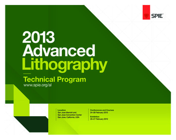
Technical Programwww.spie.org/alLocationSan Jose Marriott andSan Jose Convention CenterSan Jose, California, USAConferences and Courses24–28 February 2013Exhibition26–27 February 2013
WelcomeYour attendance at SPIE Advanced Lithographyincreases your company’s success in the lithographyindustry through access to the latest research,networking opportunities, and technology on display.SPIE would like to express its deepestappreciation to the symposium chairs,conference chairs, program committees,and session chairs who have sogenerously given their time and advice tomake this symposium possible.Technical ProgramConferences and Courses: 24–28 February 2013 · Exhibition: 26–27 February 2013San Jose Marriott and San Jose Convention Center, San Jose, California, USAThe symposium, like our other conferencesand activities, would not be possiblewithout the dedicated contribution of ourparticipants and members. This programis based on commitments received up tothe time of publication and is subject tochange without notice.
ContentsTechnical ConferencesWelcome . . . . . . . . . . . . . . . . . . . . . . . . . . . . . . . . . . . . . . . . . 2Sponsors . . . . . . . . . . . . . . . . . . . . . . . . . . . . . . . . . . . . . . . . 3Floor Plans . . . . . . . . . . . . . . . . . . . . . . . . . . . . . . . . . . . . . . . 4Daily Schedule . . . . . . . . . . . . . . . . . . . . . . . . . . . . . . . . . . . . 5Events, ConferencesPlenary Presentations . . . . . . . . . . . . . . . . . . . . . . . . . . . . 6–7Special and Technical Events . . . . . . . . . . . . . . . . . . . . . . 6–8Award Announcements . . . . . . . . . . . . . . . . . . . . . . . . . . . . . 9Exhibition Information . . . . . . . . . . . . . . . . . . . . . . . . . . . . . 10General Information . . . . . . . . . . . . . . . . . . . . . . . . . . . . 11–14Course Schedule . . . . . . . . . . . . . . . . . . . . . . . . . . . . . . . . . 15Technical Conference Session Schedule . . . . . . . . . . . 16–17Index of Authors, Chairs, and Committee Members . . 54–65Proceedings of SPIE . . . . . . . . . . . . . . . . . . . . . . . . . . . . . . 66Extreme Ultraviolet (EUV) Lithography IV(Naulleau, Wood) . . . . . . . . . . . . . . . . . . . . . . . . . . . . . . 18-48Alternative Lithographic Technologies V(Tong, Resnick) . . . . . . . . . . . . . . . . . . . . . . . . . . . . . . . . 18-52Metrology, Inspection, and Process Controlfor Microlithography XXVII (Starikov, Cain) . . . . . . . . 18-52Advances in Resist Materials and ProcessingTechnology XXX (Somervell, Wallow) . . . . . . . . . . . . . 18-43Optical Microlithography XXVI(Conley, Lai) . . . . . . . . . . . . . . . . . . . . . . . . . . . . . . . . . . 19-53Design for Manufacturability throughDesign-Process Integration VII (Mason,Sturtevant) . . . . . . . . . . . . . . . . . . . . . . . . . . . . . . . . . . . 19-53Advanced Etch Technology forNanopatterning II (Zhang, Oehrlein, Lin) . . . . . . . . . . . 19-31Sponsored by 1 360 676 3290· help@spie.org·#SPIELitho1
Welcome!Executive CommitteeJason P. Cain, Advanced Micro Devices, Inc.Will Conley, Cymer, Inc.Mircea V. Dusa, ASML US, Inc.Kafai Lai, IBM Corp.Harry J. Levinson, GLOBALFOUNDRIES Inc.Mark E. Mason, Texas Instruments Inc.Patrick P. Naulleau, Lawrence Berkeley National Lab.Gottlieb Oehrlein, Univ. of Maryland, College ParkDouglas J. Resnick, Molecular Imprints, Inc.Mark H. Somervell, Tokyo Electron America, Inc.Alexander Starikov, I&I ConsultingJohn L. Sturtevant, Mentor Graphics Corp.William M. Tong, KLA-Tencor CorpThomas I. Wallow, GLOBALFOUNDRIES Inc.Obert R. Wood II, GLOBALFOUNDRIES Inc.Ying Zhang, Taiwan Semiconductor Manufacturing Co., Ltd.Advisory CommitteeRobert D. Allen, IBM Almaden Research Ctr.William H. Arnold, ASML US, Inc.Timothy A. Brunner, IBM Thomas J. Watson Research Ctr.Ralph R. Dammel, AZ Electronic Materials USA Corp.Roxann L. Engelstad, Univ. of Wisconson, MadisonDonis G. Flagello, Nikon Research Corp. of AmericaHarry J. Levinson, GLOBALFOUNDRIES Inc.Burn Lin, Taiwan Semiconductor Manufacturing Co., Ltd.Chris A. Mack, lithoguru.comWilhelm Maurer, Infineon Technologies AGChristopher J. Progler, Photronics, Inc.Michael T. Postek, National Institute of Standards and TechnologyLuc Van den hove, IMECC. Grant Willson, The Univ. of Texas at AustinAnthony Yen, Taiwan Semiconductor Manufacturing Co., Ltd.2Today, lithographers are challenged with cost-effectively extending immersionlithography to physical limits using multi-exposure and multiple-etch processes,while striving to bring newer technologies, such as EUV lithography, to productionreadiness. Success will demand unprecedented ingenuity, cost efficiency, andcommunication within the lithography community and across interdisciplinary lines.For the past 37 years, SPIE Advanced Lithography has played a key role in bringingthe lithography community together to solve challenges required by the semiconductorindustry. Symposium participants come from an extensive array of backgrounds toshare and learn about state-of-the-art lithographic tools, resists, metrology, materialscharacterization, and design and process integration.SPIE Advanced Lithography is organized into seven conferences: Alternative Lithographic Technologies Extreme Ultraviolet Lithography Metrology, Inspection, and Process Control for Microlithography Advances in Resist Materials and Processing Technology Optical Microlithography Design for Manufacturability through Design-Process Integration Advanced Etch Technology for NanopatterningAll conferences are organized by current practitioners of the art, and numerouscourses are taught by recognized industry experts. Additional information is availablefrom the many manufacturers’ exhibits, which allow tool makers and material andsoftware suppliers to showcase new products while interacting one-on-one withcustomers. Through a series of thought-provoking panel discussions and seminars,the symposium further probes current issues to be faced as we extend thesetechnologies or try to switch to alternative technologies.We welcome you to the San Jose Convention Center, San Jose, California, for SPIEAdvanced Lithography’s 38th year!Harry J. LevinsonGLOBALFOUNDRIES Inc.2013 Symposium ChairSPIE Advanced Lithography 2013·www.spie.org/alMircea V. DusaASML US, Inc.2013 Symposium Co-Chair
Thanks to the following sponsors for their generous support of SPIE Advanced LithographyWi-FiTuesday Lunch Co-SponsorPlenary Sessionwww.asml.comwww.dow.comAdvanced Etch Technology forNanopatterning II comExtreme Ultraviolet (EUV) Lithography IV ConferenceAdvances in Resist Materials andProcessing Technology XXIV Conferencewww.cymer.comLanyardswww.mentor.comMeter Boardwww.hitachi-hta.comConference Bagwww.tokamerica.comAlternative Lithographic Technologies erence Bag PenStairway Stripswww.azem.comwww.fujifilm-ffem.comCoffee Breakwww.nikonprecision.comBannerExhibitor r.comwww.hitachi-hta.comExhibition BagTuesday Poster Receptionwww.tel.comwww.smt.zeiss.com/smsWednesday Poster ReceptionLuggage Breakfast Sponsorwww.azem.comwww.appliedmaterials.comHotel Room Keywww.appliedmaterials.comGeneral t PavilionOptical Microlithography XXVI Conferencewww.jeolusa.com 1 360 676 3290www.cymer.com· help@spie.org · #SPIELithoASMLHitachi High TechnologiesMicro Lithography Inc.Solid State TechnologyTNO Science and Industry3
San JoseConvention Centerand Marriott Hotel214213San Jose Convention CenterExhibit and Meeting Room Level212210231211ExhibitionHall 1Down to Rooms111–114Speaker Check-in DeskInternet PavilionSPIE MarketplaceHall 2111112San Jose Marriott, Second Floor114Hall 3Hilton HotelThird Floor113233232Exhibitor RegistrationAttendee RegistrationMarriottSalons4230SPIE Advanced Lithography 2013·www.spie.org/al
Daily ScheduleSundaySpecial EventsMondayTuesdayWelcome and Announcements (Levinson),8:00 to 8:40 am, p. 6Plenary presentation: Contact Printing toEUV: Lessons Learned from the Art ofLithography (Siegle) 8:40 to 9:10 am, p. 6Plenary presentation: The Evolution ofEDA Alongside Rapid Silicon TechnologyInnovation (Ko) 9:10 to 9:50 am, p. 7Plenary presentation: The New U.S. PatentLaw: What You Need to Know and HowIt Will Affect Your Strategy (Szmanda,Shelnut) 9:50 to 10:30 am, p. 7WednesdayExhibition, p. 1010:00 am to 5:00 pm 10:00 am to 4:00 pmPanel Discussion on Challenges forDirected Self-Assembly (Cheng, Tong)5:00 to 7:00 pm, p. 8Poster Reception (Conferences 8681,8682, 8685) 6:00 to 8:00 pm, p. 8Joint Panel Discussion (Joint Panel withconfs. 8679, 8680, 8682, 8683, 8684), 7:30to 9:00 pm, p. 8Poster Reception (Conferences 8679,8680, 8683, 8684) 6:00 to 8:00 pm, p.8Panel Discussion on Making aBusiness Case for Disruptive MetrologyTechnologies: What Should We InvestIn? (Vaid, Bunday, Sendelbach) 7:30 to9:00 pm, p. 8ThursdayPresentation of the Best Student PaperAward in Microlithography, 10:30 to10:40 am, p. 92013 Best Student Paper Award inMetrology, 10:30 to 10:40 am, p. 9Award Announcements for Conferenceon Metrology, Inspection, and ProcessControl for Microlithography, 11:00 to11:20 am, p. 9Award Announcements for Conferenceon Advances in Resist Materials andProcessing Technology, 11:00 to 11:20am, p. 9Nanotechnology in MicrolithographyPanel Discussion, Approaching the Limitsof 3D Metrology: Are There Any SolutionsBeyond 14 nm? (Silver, Barnes, Bunday)6:00 to 7:30 pm, p. 8ConferencesConf. 8679 Extreme Ultraviolet (EUV) Lithography IV (Naulleau) p. 18-48Conf. 8680 Alternative Lithographic Technologies V (Tong) p. 18-52Conf. 8681 Metrology, Inspection, and Process Control for Microlithography XXVII (Starikov) p. 18-52Conf. 8682 Advances in Resist Materials and Processing Technology XXX (Somervell) p. 18-43Conf. 8683 Optical Microlithography XXVI (Conley) p. 19-53Conf. 8685 Advanced Etch Technology for Nanopatterning II (Zhang) p. 19-31Conf. 8684 Design for Manufacturability through Design-Process Integration VII(Mason) p. 19-53See Course DailySchedule, page 15. 1 360 676 3290· help@spie.org·#SPIELitho5
Special EventsWelcome and AnnouncementsPlenary Presentations · Convention Center Hall 3Convention Center Hall 38:40 to 9:10 amMonday 25 February. . . . . . . . . . . . . 8:00 to 8:40 amSymposium Chair: Harry J. Levinson,GLOBALFOUNDRIESContact Printing to EUV: Lessons Learnedfrom the Art of LithographyIntroduction of New SPIE Fellows10th Frits Zernike Award for Advances inOptical MicrolithographyAward Sponsored by:6William T. Siegle, IndependantConsultant and ASML Advisory BoardMemberWe have all had the privilege of working in anelectronics industry that has shown stunningadvances. Over the last 50 years, wehave watched a progression from discretetransistors and simple ICs, to powerfulcomputers we all carry in our pockets. This progress wouldnot have been possible without equally remarkable progressin semiconductor lithography, the art of creating patternson silicon to form these circuit patterns.Through my career at IBM, AMD, and Board membershipsat Etec, DuPont Photomasks, and ASML, I have been bothobserver, participant, and user of lithography. The enormousprogress in both the IC technology and the accompanyinglithography techniques has provided many “teachingmoments”. It is my privilege to share some of the lessonsgleaned from this experience. While some of these lessonsare peculiar to our arcane art, others may be more broadlyapplicable.The first era of lithography practiced “1 to 1” printing. Thatis, mask patterns and wafer images were dimensioned in aone-to-one relationship. Initially practiced through contactprinting in the 60s, moving to 1x projection in the 70s, thispractice served well until demands on mask fidelity becametoo great, and reduction alternatives became available.As wafer sizes grew, and feature sizes shrank, opticalreduction techniques and “step and repeat” of sub waferfield sizes ruled the day. Once robust steppers becamewidely available, the race turned to reducing wavelength and“wave front engineering” to deliver smaller features. Withexposure wavelengths currently limited to 193nm, exhaustedlitho engineers are resorting to multiple patterning to escapethe trauma of ridiculously low k1 values.SPIE Advanced Lithography 2013·www.spie.org/alEUV with its 13.5nm wavelength promises relief from193nm limits. While prototype machines are operatingin a number of customer fabs, the productivity requiredfor economical manufacturing insertion has not yet beendemonstrated. Other alternatives, such as e- beam ornanoimprint have shown promising laboratory results, andshow lots of activity at this conference each year. But aviable path to production insertion for these alternativesis not visible, and substantial industrialization investmentwould be required.Never-the-less, the dedication and ingenuity of ourworldwide talents always seems to find a way. Many lessonshave been learned, with in all likelihood, more to come.Bill (William T.) Siegle attended Rensselaer Polytechnic,and he received his Ph. D. in Electrical Engineering in1964.He enjoyed a 25 year career at IBM where he became theDirector of the Advanced Technology Center in East Fishkill.He joined Advanced Micro Devices in Sunnyvale in 1990 asVice President of Technology, and retired in 2005 as Sr. VPof Technology and Manufacturing. He has served on theboards of SRC and Sematech, and the public companiesEtec, DuPont Photomasks and currently ASML. He has beeninvolved with lithography throughout his career, as both anenabler and a user.
Plenary Presentations Sponsored by:9:10 to 9:50 am9:50 to 10:30 amThe Evolution of EDA Alongside RapidSilicon Technology InnovationThe New U.S. Patent Law: What YouNeed to Know and How It Will Affect YourStrategyHoward Ko, Senior VP and GeneralManager, Synopsys’ Silicon EngineeringGroupThe overall product design andmanufacturing flow needed to create anew advanced semiconductor device isone of the most economically successfuland most complex industrial ecosystems in the world. Theongoing economic success is especially amazing whenone considers the enormous changes which occurs in thiscomplex ecosystem every technology generation. SPIEattendees know full well the many important difficulties andchallenges involved in continuing the rapid pace of costeffective lithography and silicon process development. Justas critical, however, are the challenges which designers andEDA suppliers face to modify and re-architect their designflows and design tools to best incorporate the outcomesof this rapid technology improvement. The goal of this talkis to provide high level insight into the continuing evolutionwhich the EDA industry has done and must continue todo in order to keep pace with the hectic pace of silicontechnology innovation.Dr. Howard Ko joined Synopsys in June 2002 and iscurrently Senior Vice President and General Manager ofthe Silicon Engineering Group. He manages productsand solutions that address semiconductor manufacturingtechnology needs. These solutions include TCAD, yieldmanagement, failure analysis, mask data preparation,Optical design and analysis, Photonics design, lithographysimulation, and mask patterning. In his previous role as VicePresident of Sales, Asia Pacific, Dr. Ko built a continuouslyincreasing revenue stream, improved Synopsys’ leadershipposition in the region, and increased collaboration withleading foundries. Before joining Synopsys, Dr. Ko servedas Avant!’s executive operating officer since July 2001.Previously, he was general manager of Avant!’s mixedtechnology division and head of the system product line. Dr.Ko has also held senior management roles at Analogy, Inc.and Mentor Graphics. Dr. Ko received his Ph.D. in ElectricalEngineering and Computer Science from UC Berkeley, andgraduated with a B.S. degree in Electrical Engineering fromthe National Taiwan University.Charles R. Szmanda, James G.Shelnut,The Patent Practice of Szmanda,Shelnut, LLCOver the years, the electronic patterningarts have been characterized by a businessenvironment that incorporates features ofpre-competitive cooperation during theearly phases of development and intensecompetition during the later phases. Cooperative activitiessuch as pre-competitive development, joint developmentagreements, road-mapping activities, and the sharingof resources are commonplace. Moreover, while theelectronics industry is intensely competitive during laterstages of development and production, the willingness ofmany industry players to license and cross license patentedtechnologies has promoted rapid technological developmentfor decades in ways not seen in other industries. Thisbusiness environment, and the old patent laws based on“first-to-invent” priority, have formed a basis for manycurrent intellectual property strategies.In this talk, we review briefly what a patent is and what isrequired to get one. We then describe the most importantaspects of the new patent law. These include: (1) the “firstinventor to file” system, which takes effect on March 16,2013 and replaces the “first to invent” system in currentlaw; (2) new ways to challenge issued patents such as“Post Grant Review” and “Inter Partes” review; (3) prior artsubmission during prosecution of another inventor’s patentapplication; (4) prioritized examination of applications; and(5) prior user rights. We go on to discuss how these newelements of the law will alter the competitive environment butwill also present a number of opportunities for formulatinga successful patent strategy within that new environment. 1 360 676 3290· help@spie.org·#SPIELithoWe conclude by offering several suggestions forformulating a practical patent strategy in view of the newlaws. We show how publishing at the wrong time candestroy your right to get a patent but publishing at theproper time can enhance your competitive position. Wefurther show how you can protect your right to practicetrade secrets that you choose not to patent. Finally, weshow how the law provides opportunities to challenge patentclaims submitted by competitors both before and after thepatent is granted.Charles R. Szmanda is a principal partner at the PatentPractice of Szmanda & Shelnut, LLC. He has been a patentagent, for over 12 years and is registered to practice beforethe United States Patent and Trademark Office and theCanadian Intellectual Property Office.Szmanda spent many years in research and development,most recently as a Research Fellow at the Dow ElectronicMaterials Company, where he worked on electronicapplications of nanotechnology and did research onphotoresist materials. During his career, he designedprocesses for making silicon devices at Bell Labs,did polymer research for micro and nanolithography,helped found a startup company called Aspect Systems,did fundamental research on electron transfer duringmolecular collisions, practiced the wonderful art of x-raycrystallography and generally had a lot of fun. He holds31 U.S. patents and is the author of over 60 scientificpublications.Szmanda holds a B.S. in chemistry from Loyola Universityand a Ph.D. in physical chemistry from the University ofWisconsin.In his off hours, he continues to blow the hell out of hisflugelhorn whenever he can put a band together.7
Technical EventsNanotechnology in MicrolithographyPanel DiscussionPanel Discussion on Challenges forDirected Self-AssemblyConvention Center Room 210 BConvention Center Hall 3Monday 25 February. . . . . . . . . . . . . . . . . 6:00 to 7:30 pmTuesday 26 February. . . . . . . . . . . . . . . . 5:00 to 7:00 pmModerators: William M. Tong, KLA-Tencor Corp. and JoyY. Cheng, IBM Almaden Research Ctr.Approaching the Limits of 3D Metrology: Are ThereAny Solutions Beyond 14 nm?Moderators: Richard M. Silver, Bryan Barnes, NationalInstitute of Standards and Technology; Benjamin Bunday,International SEMATECHPoster ReceptionsConvention Center Hall 2Tuesday 26 February. . . . . . . . . . . . . . . . . 6:00 to 8:00 pm(Conferences 8679, 8680, 8683, 8684)Tuesday Poster Reception SponsorThe Exhibition will be open during the Poster Reception onTuesday only. Be sure to visit the exhibit booths during thistime for insight on what is new or coming soon!Convention Center Hall 2Wednesday 27 February. . . . . . . . . . . . . . 6:00 to 8:00 pm(Conferences 8681, 8682, 8685)Wednesday Poster Reception SponsorsDirected self-assembly (DSA), which combines lithographydefined pre-patterns with self-assembled phase-separatedpolymers, has become a promising path to continuethe scaling of semiconductor devices. As a materialsbased resolution enhancement technique, DSA has beendemonstrated to augment the patterning capability of 193i,EUV and E-beam lithography, and has begun to transitionfrom research labs to development lines in past twoyears. While there have been important advances on thematerials and process fronts, to enable DSA as a resolutionenhancement technology, more efforts are required inareas such as DSA-aware design and low defectivity.The characteristic length and nature of phase-separatedpolymers impose DSA-specific design restrictions anddesign-related defectivities. The integration of compactDSA model into design and computational lithographymay facilitate the co-optimization of design, materials, andprocesses. On the defectivity front, more experimental dataon inspection, metrology and unit process monitoring areneeded to identify the defect sources and intrinsic DSAdefects. Please join experts in design, DFM, metrology,and other critical areas in DSA to discuss these criticalchallenges for DSA.Panel Discussion on Making aBusiness Case for Disruptive MetrologyTechnologies: What Should We Invest In?Convention Center Room 230 BWednesday 27 February. . . . . . . . . . . . . . 7:30 to 9:00 pmModerators: Alok Vaid, GLOBALFOUNDRIES, Inc.;Benjamin D. Bunday, SEMATECH North; Matthew J.Sendelbach, Nova Measuring Instruments, Inc.Continuing decrease in the device dimensions, combinedwith complex disruptive materials and 3D architectureshave placed increasing demands on metrology tools.Over the years, the industry has implemented severalinnovative solutions to alleviate these challenges, but mostof them have been incremental improvements rather thanrevolutionary. There seems to be inertia preventing theadoption of revolutionary and disruptive measurementtechniques, some of which have been in the limelight forabout a decade. The panel will focus on three key disruptivesolutions which have been identified as potential nextgeneration metrology and inspection technologies for sometime – CD-SAXS, Multi-ebeam-based inspection, and He-ionimaging. Our panel of experts will come from a mix of ICmanufacturers, suppliers, academia, research consortia andventure capitalist firms. Panelists will review the technical,business and financial aspects of these technologies andalso try to form a consensus on whether they are reallyneeded to meet current industry requirements. The panel willrecommend whether the industry should continue to investin these technologies, and if so, then what it will “actually”take to get them implemented in HVM.Joint Panel DiscussionConvention Center Hall 3All registered attendees are invited to attend the postersessions. Come view the high-quality papers that arepresented in this alternative format, and interact with theposter authors who will be available for discussion. Enjoylight refreshments while networking with colleagues in yourfield.Attendees and authors are required to wear theirconference registration badges to the poster sessions.Tuesday 26 February. . . . . . . . . . . . . . . . . 7:30 to 9:00 pmJoint Panel with conferences 8679, 8680, 8682, 8683, 8684SPIE Advanced Lithography Promotional PartnersMazik MediaMEMS and Nanotechnology ExchangePhotonics MediaPhotonics OnlineSolid State Technology8SPIE Advanced Lithography 2013·www.spie.org/al
Award AnnouncementsSPIE Apps for iPhoneand Android Conference ProgramAward Announcements for Conferenceon Metrology, Inspection, and ProcessControl for MicrolithographyAward Announcements for Conferenceon Advances in Resist Materials andProcessing TechnologyConvention Center Room 230 BConvention Center Hall 3Monday 25 February . . . . . . . . . . . . . . 11:00 to 11:20 amMonday 25 February. . . . . . . . . . . . . . . 11:00 to 11:20 amPresentation of the 2012 Diana NyyssonenMemorial Award for Best Paper in MetrologyAward Sponsored byPresentation of the 2012 Hiroshi Ito MemorialAward for the Best Student Paper in ResistAndroid and iPhone Create your schedule—searchand browse the TechnicalProgram and special events,participants, and exhibitors.ProfilesPresentation of the 2012 C. Grant WillsonAward for Best Paper in ResistThese Awards Sponsored byPresentation of the 2013 Best StudentPaper Award in MetrologyiPhone Convention Center Room 230 BMake valuable personalconnections— find andcontact colleagues based onSPIE research publications,conference involvement, andcourses taught.Thursday 28 February. . . . . . . . . . . . . . 10:30 to 10:40 amAward Sponsored byField GuidesPresentation of the 2012 Jeffrey ByersMemorial Best Poster Award in ResistAward Sponsored byAward Announcement for Conference8683—Optical MicrolithographyAndroid and iPhone Take Field Guides to a newlevel—access and useequations, linked terms,bookmarks, and interactivefigures, and take notes.Try Geometrical Optics Field Guide Lite for Free!Convention Center Room 210 CThursday 28 February. . . . . . . . . . . . . . 10:30 to 10:40 amPresentation of the 2013 Best Student Awardin MicrolithographyNewsroomAward Sponsored byAndroid and iPhone The latest innovations, news, and multimediacoverage of Optics and Photonics.iPhone and iTunes are registered trademarks of Apple Inc. 1 360 676 3290· help@spie.org·#SPIELitho9
Visit the exhibition. See the latest lithographyresearch and development, devices,tools, fabrication, and services.ExhibitionConvention Center Hall 1Tuesday 26 February10:00 am to 5:00 pm;Poster reception:6:00 to 8:00 pmWednesday 27 February10:00 am to 4:00 pmExhibitionTechnologiesLithography: immersion,double patterning, e-beam,EUV, optical/laser, and RETMetrology, inspection, OPC,and process controlDesign and manufacturingsoftwareMaterials and chemicalsImaging equipmentLasersResist materials andprocessingNano-imprintIC and chip fabricationNanoscale imaging10Ibss Group, Inc.Inko Industrial Corp.Inspectrology LLCJ.A. Woollam Co., Inc.JSR Micro, Inc.King Industries, Inc.MEMS & NanotechnologyExchangeMentor Graphics Corp.Micro Lithography, Inc.MicroChem Corp.micro resist technology GmbHMirero Inc.Mitsui Chemicals America, Inc.Molecular Imprints, Inc.Nanometrics Inc.OMG CyantekOptical Support, Inc.Opto Diode Corp.Owens DesignPall Corp.Photonics Online2013 Exhibiting Company list(Current as of 1/21/2013)Abeam TechnologiesAmuneal Manufacturing Corp.ASMLattocube systems Inc.Benchmark TechnologiesBrewer Science Inc.Brion TechnologiesCapitol Scientific MicrofabricationMaterialsCarl Zeiss SMS GmbHDNS Electronics, LLC / SCREEN /SOKUDOEnergetiq Technology, Inc.Fortrend EngineeringFUJIFILM Electronic MaterialsGenISys GmbHGudeng Precision Industrial Co., Ltd.Halocarbon Products CorporationHeraeus DaychemContact SPIE Sales: Tel: 1 360 676 3290 · Fax: 1 360 647 1445 · teresar@spie.orgSPIE Advanced Lithography 2013·www.spie.org/alPozzettaQoniac GmbHRigaku Innovative Technologies Inc.RION Co., Ltd.Rudolph Technologies, Inc.SAES Pure GasSagemShin-Etsu MicroSiSolid State Technology / Laser FocusWorldStorex TechnologiesSumika Electronic MaterialsSynopsys Inc.TNOTokyo Ohka Kogyo America, Inc.TRIOPTICS GmbHVistec Electron Beam GmbHVistec Lithography, Inc.XEI Scientific, Inc.XyalisZygo Corporation
General InformationExhibition RegistrationExhibition-Only visitor registration is complimentary.San Jose McEnery Convention Center, 150 West San Carlos,San Jose, CA 95113 USA.RegistrationFor credentialed press and media representatives only.Please email contact information, title, and organization tomedia@spie.orgSPIE CashierLocation – San Jose Convention Center Concourse 2 LevelOpen during registration hoursSunday 24 February . . . . . . . . . . . . . . 7:00 am to 5:00 pmMonday 25 February. . . . . . . . . . . . . . 7:00 am to 4:00 pmTuesday 26 February. . . . . . . . . . . . . . 7:30 am to 5:00 pmWednesday 27 February. . . . . . . . . . . 7:30 am to 4:00 pmThursday 28 February. . . . . . . . . . . . . 7:30 am to 4:00 pmConference RegistrationIncludes admission to all conference sessions, plenaries,panels, and poster sessions, admission to the Exhibition,coffee breaks, SPIE hosted lunches Tuesday and Wednesday,and a choice of proceedings. Student pricing does notinclude proceedings.SPIE Member, SPIE Student Member, and Student Pricing SPIE Members receive conference and course registrationdiscounts. Discounts are applied at the time of registration. SPIE Student Members receive a 50% discount on allcourses. Student registration rates are available only to undergraduateand graduate students who are enrolled full time and havenot yet received their Ph.D. Post-docs may not register asstudents. A student ID number or proof of student statusis required with your registration.Speaker Check-In and Preview StationPress RegistrationOnsite Registration and Badge Pick-upHoursAuthor / Presenter InformationConvention Center Ballroom ConcourseSunday . . . . . . . . . . . . . . . . . . . . . . . 2:00 pm to 6:00 pmMonday through Thursday . . . . . . . . .7:30 am to 5:00 pmAll conference rooms have a computer workstation, projector,screen, lapel microphone, and laser pointer. All presenters arerequested to come to Speaker Check-In with their memorydevices or laptops to confirm their presentation displaysettings.Registration AreaR
William H. Arnold, ASML US, Inc. Timothy A. Brunner, . Tuesday Poster Reception www.tel.com Wednesday Poster Reception eption www.azem.com www.tokamerica.com Internet Pavilion . Speaker Check-in Desk Internet Pavilion SPIE Marketplace Exhibition Hall 1 Hall 2H all 3 232 231 233 Down to Rooms 111-114 213 214 211