Transcription
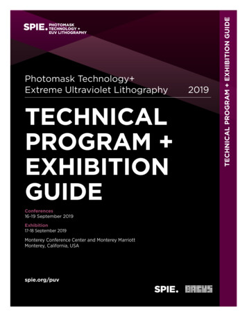
TECHNICALPROGRAM EXHIBITIONGUIDEConferences16-19 September 2019Exhibition17-18 September 2019Monterey Conference Center and Monterey MarriottMonterey, California, USAspie.org/puv2019TECHNICAL PROGRAM EXHIBITION GUIDEPhotomask Technology Extreme Ultraviolet Lithography
CONNECTING MINDS.ADVANCING LIGHT.PHOTOMASKTECHNOLOGY EUV LITHOGRAPHYConferences: 16-19 September 2019Exhibition: 17-18 September 2019Monterey Conference Center and Monterey MarriottMonterey, California, USAWelcome toMontereyCUTTING-EDGE RESEARCH2-DAY EXHIBITIONspie.org/puv
Plenary Presentations. . . . . . . . . . . . . page 5Don’t miss these world-class speakers discussing thelatest advancements and most promising breakthroughs.Special Events . . . . . . . . . . . . . . . . . . . page 6Join your peers and colleagues in discussions aroundfocused technical topics and networking opportunities.Exhibition. . . . . . . . . . . . . . . . . . . . . . page 8–15Meet key suppliers of components, software, andmanufacturing equipment.Sponsors. . . . . . . . . . . . . . . . . . . . . . page 16-17See the organizations helping to support the industry and this event.Conferences. . . . . . . . . . . . . . . . . . . page 18-27EXTREME ULTRAVIOLET LITHOGRAPHYCONFERENCE . . . . . . . . . . . . . . . . . . . . . . . . . . . . . . . . . . . . page 18-26PHOTOMASK TECHNOLOGY CONFERENCE . . . . . . . . . page 18-27Awards Information . . . . . . . . . . . . page 26Announcing the 2019 Photomask Student Awards.SPIE is the international society for optics and photonics, aneducational not-for-profit organization founded in 1955 toadvance light-based science and technology. The Society servesnearly 264,000 constituents from approximately 166 countries,offering conferences and their published proceedings, continuingeducation, books, journals, and the SPIE Digital Library insupport of interdisciplinary information exchange, professionalnetworking, and patent precedent. SPIE provided more than 4million in support of education and outreach programs in 2018.INDEX OF AUTHORS, CHAIRS, ANDCOMMITTEE MEMBERS . . . . . . . . . . . . . . . . . . . . . . . . . . . . page 88-31GENERAL INFORMATION . . . . . . . . . . . . . . . . . . . . . . . . . page 32-33SPIE POLICIES. . . . . . . . . . . . . . . . . . . . . . . . . . . . . . . . . . . . page 34-35For more information, visit SPIE.org.1
LunchPostersMONTEREY CONFERENCE CENTER AND MARRIOTT FLOOR PLANGet the free SPIE Conferenceand Exhibition AppFind the best networking and information-gatheringopportunities with this powerful planning tool. Scheduleyour time in the conferences navigate the exhibition floor make new connections.Available for iOS and Android.Search: SPIE Conferences.2SPIE Photomask Technology Extreme Ultraviolet Lithography 2019·spie.org/puv· #SPIEPhotomaskEUV
PHOTOMASK TECHNOLOGY AND EXTREME ULTRAVIOLETLITHOGRAPHY CONFERENCE SCHEDULETIMECONF. 11147:CONF. 11148:International Conference on Extreme UltravioletLithography 2019 (Itani, Gargini, Naulleau, Ronse )Photomask Technology (Rankin, Preil)MONDAY 16 SEPTEMBERAMSESSION 1:Plenary Session chair (Rankin, Kozawa)SESSION 1:Plenary Session chairs (Rankin, Kozawa)SESSION 2:EUV Scanner, Source, and Industrialization (Kaiser, Lee)SESSION 2:Survey (Rankin, Preil)SESSION 3:Mature Mask Support (Rankin, Preil)LunchPMSESSION 3:EUV Stochastic I (Wallraff, Hendrickx)SESSION 4:Deep Learning Mask Applications (Fujimura, Sun)SELECTED POSTER SPEED TALKS (JOINT SESSION) (Location: Monterey Conference Center, Steinbeck 2/3 )MONDAY POSTER SESSION (Location: Monterey Marriott, San Carlos Ballroom 4)TUESDAY 17 SEPTEMBERAMSESSION 4:EUV Mask and Lithography Integration (Abboud, Jonckheere)SESSION 5:EUV Mask and Lithography Integration (Abboud, Jonckheere)SESSION 5:EUV Resist I (Dai, Fujimori)SESSION 6:Mask Writer and Mask Process Correction (MPC)(Behringer, Shusuke)Lunch/Exhibition BreakPMSESSION 7:Processing, Photoresist, and NanoImprint Lithography(Faure, Sharma)SESSION 8:Mask Data Prep MPD and Curvlinear Data Handling(Buck, Hayashi)NO SESSIONS SCHEDULEDWEDNESDAY 18 SEPTEMBERAMSESSION 6:EUV Blank and Films (Takahiro, Liang)SESSION 9:EUV Blank and Films (Takahiro, Liang)SESSION 7:EUV Defects, Inspection, and Characterization(Scherübl, Jindal)SESSION 10:EUV Defects, Inspection, and Characterization (Scherübl, Jindal)Lunch/Exhibition BreakPMSESSION 8:EUV Pellicle (Gallagher, Hayashi)SESSION 11:EUV Pellicle (Gallagher, Hayashi)SESSION 9:EUV Resist and Material (Kozawa, Graeupner)Panel Discussion: Mask Ecosystem for Low-k1 EUVManufacturing: Beyond First Generation EUV Single PatteringTHURSDAY 19 SEPTEMBERAMSESSION 10:Hi-NA and EUV Imaging (Troost, Levinson)NO SESSIONS SCHEDULEDSESSION 11:EUV Stochastic II and Future (Ronse, De Silva)THIS PROGRAM IS CURRENT AS OF 26 AUGUST 2019. FIND THE LATEST ON THE SPIE CONFERENCE APP.3
WELCOMEThe Photomask Technology and the Extreme Ultraviolet Lithography conferences will come together throughout the weekwith joint sessions.As conference chairs, we welcome you to beautiful Monterey!INTERNATIONAL CONFERENCE ONEXTREME ULTRAVIOLET LITHOGRAPHYSPIE PHOTOMASK TECHNOLOGYThe 39th Photomask Conference, organized by SPIE incooperation with BACUS Steering Committee, is the globalforum for scientists, engineers, and industry leaders to presentand discuss key topics related to photomasks. The conferenceaddresses design, fabrication, quality control, and the use ofphotomasks in the semiconductor industry.The International Conference on Extreme Ultraviolet Lithographyprovides a forum to discuss and assess the worldwide statusof EUV technology and infrastructure readiness. Scientists,engineers, and industry leaders meet to present and discuss newand unpublished materials.Toshiro ItaniOsaka Univ. (Japan)2019 EUV Lithography Conference ChairJed H. RankinGLOBALFOUNDRIES Inc. (USA)2019 Photomask Technology Conference ChairPatrick P. NaulleauLawrence Berkeley National Lab. (United States)2019 EUV Lithography Conference ChairMoshe E. PreilKLA-Tencor Corp.(USA)2019 Photomask Technology ConferenceCo-ChairPaolo A. GarginiStanford Univ. (United States)2019 EUV Lithography Conference Chair2019 BACUS STEERING COMMITTEEFrank E. Abboud, Intel Corp.Patrick M. Martin, AppliedMaterials, Inc.Michael D. Archuletta, RAVE LLCKent Nakagawa, ToppanArtur Balasinski, CypressPhotomasks, Inc.Semiconductor Corp.Jan Hendrik Peters, bmbgUwe F. W. Behringer, UBCconsultMicroelectronicsMoshe Preil, KLA-Tencor Corp.Peter D. Buck, Mentor GraphicsCorp.Jed Rankin,GLOBALFOUNDERIES Inc.Brian Cha, Samsung ElectronicsCo., Ltd.Stephen P. Renwick, NikonResearch Corp. of AmericaDerren Dunn, IBM Corp.Douglas J. Resnick, CanonThomas B. Faure,Nanotechnologies, Inc.GLOBALFOUNDRIES Inc.Thomas Scheruebl, Carl ZeissAki Fujimura, DS2, Inc.SMT GmbHEmily E. Gallagher, imecThomas Struck, InfineonBrian J. Grenon, GrenonTechnologies AGConsultingBala Thumma, Synopsys, Inc.Jon Haines, Micron TechnologyAnthony Vacca, AutomatedInc.Visual InspectionNaoya Hayashi, Dai NipponMichael Watt, Shin-EtsuPrinting Co., Ltd.MicroSi Inc.Bryan S. Kasprowicz, Photronics,Inc.Larry Zurbrick, KeysightTechnologies,Inc. Lithography 2019SPIE Photomask Technology ExtremeUltraviolet4Kurt G. Ronseimec (Belgium)2019 EUV Lithography Conference Chair·spie.org/puv· #SPIEPhotomaskEUV
PLENARY SESSIONPlenary SessionSPONSORED BYMonday 16 September 8:00 AM - 9:50 AMLocation: Monterey Conference Center, Steinbeck 2/38:00 - 8:30 AMAnnouncements and Welcome9:10 - 9:50 AM8:30 - 9:10 AMEUV Extendibility at 0.33 and 0.55NAMark Phillips, Director of Lithography Hardwareand Solutions Intel Corp. (USA)Review of near and long term extension challenges for EUVlithography at 0.33 and 0.55NA. Focus on mask and infrastructure gaps opportunities and a review of progressmade in critical areas to support EUV extension.Dr. Phillips is an Intel Fellow and Director of Lithography Hardware andSolutions. He graduated in 1992 from Caltech with a PhD in Physics andjoined Intel in 1993 in the Technology Development organization in Oregon.Mark’s long career at the cutting edge of lithography spans pre-KrF steppersto present day EUV and Immersion tools.Chip to City: The Future of MobilityStefan Jockusch, Vice President of Siemens PLMSoftware, Siemens Digital Factory Division, (USA)Transportation is in the midst of enormous upheaval. Carcompanies and suppliers are expanding their focus to mobility services and deploying and managing vehicle fleetsto meet the needs of consumers and cities. This spurringtechnical innovation spanning semiconductors to cities, including electric,connected and autonomous design, simulation, manufacturing and fleetmanagement.Dr. Stefan Jockusch, Vice President of Strategy for Siemens PLM Software,that now includes Mentor a Siemens company, will examine how a spectrumof technology advances are emerging that will help companies to thriveduring this disruption. Specifically, he will examine how in the new age ofmobility, the success of autonomous vehicles in fleets hinges on the abilityof a system of advanced sensors and powerful SoCs to perceive and processan immense amount of data in real-time. These chips will require never-before-seen architectures to meet the power, performance, and area requiredfor autonomous drive. He will also touch on the other innovations making thisfuture possible including: vehicle system design such as light weighting andelectro-mechanical design; digital enterprise and manufacturing that supportsreconfigurable and small batch manufacturing; as well as advancements insmart city infrastructure and fleet management.THIS PROGRAM IS CURRENT AS OF 26 AUGUST 2019. FIND THE LATEST ON THE SPIE CONFERENCE APP.5
SPECIAL EVENTSPoster SessionMonday 16 September 2019 6:00 - 7:30 PMMonterey Marriott, San Carlos Ballroom 3, 4Conference attendees are invited to attend the Poster Session on Mondayevening in the Monterey Marriott, San Carlos 3 and 4. This session providesan opportunity for attendees to meet with colleagues, network, view postersand interact with the authors.Attendees are requested to wear their conference registration badges.SPONSORED BYDinner at the Monterey Bay AquariumWednesday 18 September 2019 6:00 - 9:45 PMMonterey Bay AquariumAll paid conference attendees are welcome to participate in this extraordinary opportunity to dine among the stunning exhibits that feature theabundant and colorful sea life of Monterey Bay.Please wear your technical conference badge. A paid attendee may purchase a dinner and Aquarium entry ticket for 100 for a guest when theattendee registers. Round-trip transportation to the Aquarium will beprovided.All paid conference attendees are welcome to participate in this extraordinary opportunity to dine among the stunning exhibits that feature theabundant and colorful sea life of Monterey Bay. Please wear your technicalconference badge. A paid attendee may purchase a dinner and Aquariumentry ticket for 100 for a guest when the attendee registers. Round-triptransportation to the Aquarium will be provided.About the Aquarium: Monterey Bay Aquarium is a nonprofit public aquariumin Monterey, California For more information and inspiration, visit the website at: https://www.montereybayaquarium.org/SHUTTLES TO THE MONTEREY BAY AQUARIUMBuses Load in front of the Monterey Conference Center at the flagpolesLoading starts at 5:45 pm. Buses will circulate every 15 minutesthroughout the event.SPONSORED BYPanel Discussion: Mask Ecosystem for Low-k1EUV Manufacturing: Beyond First GenerationEUV Single PatterningWednesday 18 September 2019 4:00 - 6:00 PMLocation: Monterey Conference Center, Steinbeck 22019 is clearly the year when EUV has entered high volume manufacturing(HVM). A viable mask infrastructure for this first generation of EUV is, bydefinition, in place now. While some elements of the existing infrastructure may be less than optimal, they have not prevented EUV from beingadopted in production.The panel of industry experts will focus on subsequent generations of EUVand will highlight areas where infrastructure improvement would be beneficial. Each panelist will offer a brief expert opinion of their views definingwhat they consider to be the major challenges to be addressed and when(or if) they will become critical items. Topics may cover any area of maskmanufacturing and use including mask blanks, films, processes, materials,inspection, storage, and particle and contamination control. The goal ofthe panel session is to promote wide ranging discussion between fabs,mask shops, suppliers and researchers to exchange opinions and identifykey areas for future development activity.6SPIE Photomask Technology Extreme Ultraviolet Lithography 2019·spie.org/puv· #SPIEPhotomaskEUV
The Journal of Micro/Nanolithography, MEMS, and MOEMS (JM3) publishespeer-reviewed papers on the science, development, and practice oflithographic, fabrication, packaging, and integration technologies necessary toaddress the needs of the electronics, microelectromechanical systems, microoptoelectromechanical systems, and photonics industries. The wide range ofsuch devices also includes biomedical microdevices, microfluidics, sensorsand actuators, adaptive optics, and digital micromirrors. The scope is broad tofacilitate synergy and interest between the communities served by the journal.Chris A. MackChris A. MackLithoguru.com, USAEditor-in-ChiefTOPICAL AREAS COVERED BY JM3 INCLUDE:Lithography: tools, materials, and processes associated with the patterning of structures that have submicrometer and nanometer-scalefeatures. Included are imaging and nonimaging approaches using optics,electron and other particle beams, nanoimprint, molecular self-assembly,and their hybrids. Applications include semiconductor fabrication, butalso patterning for other micro/nanodevices.Microelectromechanical systems (MEMS): the design, fabrication, operation, reliability, and testing of microdevices that contain both electricaland mechanical elements.Senior EditorsWilliam H. Arnold, Eikonal, USAYu-Cheng Lin, National ChengKung Univ., TaiwanMoshe Preil, KLA-Tencor, USAHarald Schenk, Fraunhofer Inst.für Photonische Mikrosysteme,GermanyThomas J. Suleski, Univ. of NorthCarolina at Charlotte, USAAssociate EditorsVivek Bakshi, EUV Litho Inc., USAMartin Burkhardt, IBM Corp., USAStefano Cabrini, The MolecularFoundry, USARalph Dammel, EMD PerformanceMaterials, USADavid L. Dickensheets, MontanaState Univ., USAHiroshi Fukuda, Hitachi HighTechnologies Corp., JapanGregg Gallatin, ASML, USARoel Gronheid, KLA, BelgiumSteven Hansen, ASML, USAStephen M. Kuebler, Univ. ofCentral Florida, USATimothy P. Kurzweg, Drexel Univ.,USAChengkuo Lee, National Univ. ofSingapore, SingaporeMicro-optoelectromechanical systems (MOEMS): the design, fabrication,operation, reliability, and testing of microdevices that contain electrical,mechanical, and optical elements (that is, the merging of micro-opticsand MEMS).Microfabrication: technologies to shape three-dimensional structuresleading to the fabrication of active and passive electronics, photonics,MEMS, MOEMS, micro/nano-optics, and other micro/nanodevices.Metrology: metrology and process control for the above devices and theirfabrication processes.Sheng-Shian Li, National TsingHua Univ., TaiwanLars Liebmann, Tokyo ElectronLimited Technology CenterAmerica, USAQinghuang Lin, ASML, USARoya Maboudian, Univ. ofCalifornia, Berkeley, USADan Meisburger, Tec-StartConsulting, USAMoses Noh, Drexel Univ., USADouglas J. Resnick, CanonNanotechnologies, Inc., USAKurt Ronse, IMEC, BelgiumMartha Sanzchez, IBM Research –Almaden, USARichard M. Silver, NIST, USAStefan Sinzinger, Technische Univ.Ilmenau, GermanyDaniel G. Smith, Nikon ResearchCorp., USAJeffry Sniegowski, Sandia NationalLaboratories, USAAlexander Starikov, I&I Consulting,USADeepak Uttamchandani, Univ. ofStrathclyde, UKWanjun Wang, Louisiana StateUniv., USAHans Zappe, Univ. of .orgTHIS PROGRAM IS CURRENT AS OF 26 AUGUST 2019. FIND THE LATEST ON THE SPIE CONFERENCE APP.7
FREE OPEN TO ALLATTENDEESSPIE Photomask Technology Extreme Ultraviolet LithographyDon’t miss your chance to speak face-to-face with suppliersEXHIBITION DATES AND HOURSLocation: Monterey Conference Center, Steinbeck 1Tuesday 17 September 2019 . . . . . . . . . . . . . . 10:00 AM - 4:00 PMWednesday 18 September 2019. . . . . . . . . . . 10:00 AM - 4:00 PMSTAY UP TO DATE ON INDUSTRY TRENDS. SEETHE LATEST IN: Mask technologies: Inspection/repair, Metrology, CleaningMask businessEUVNanoimprintDirect writePatterningWafersToolsSimulationResists and substratesMaterials and etching“This conference is critical for getting the core peopletogether to have discussions. The exchange of technologyreally helps us to innovate new technologies and that’s whatwe need with all these emerging markets.”— Petrie Yam, KLA-Tencor8SPIE Photomask Technology Extreme Ultraviolet Lithography 2019·spie.org/puv· #SPIEPhotomaskEUV
EXHIBITION 302203204EXHIBITOR BOOTH INDEX213 Shin-Etsu MicroSi, Inc.306 GenISys Inc.203 NTT AdvancedTechnology Corp.214 MSP Corp.306 Heidelberg Instruments204 Mitsui Chemicals America, Inc.215 XYALIS307 CyberOptics Corp.216 JENOPTIK Light & Optics308 Micro Lithography, Inc.207 Gudeng PrecisionIndustrial Co., Ltd.219 RAVE Mask Repair BusinessUnit, Bruker Semiconductor,Bruker Nano, Inc.312 Rigaku InnovativeTechnologies, Inc.208 INKO Industrial Corp.302 Fine Semitech Co., Ltd.209 Carl Zeiss SMT GmbH304 Energetiq Technology, Inc.210 ESTION Technologies GmbH305 ibss Group, Inc.112Semiconductor Digest206 HORIBA Instruments Inc.313 attocube systems Inc.314 Pozzetta, Inc.318 Nippon Control System Corp.320 Nano-Master, Inc.THIS PROGRAM IS CURRENT AS OF 26 AUGUST 2019. FIND THE LATEST ON THE SPIE CONFERENCE APP.9
EXHIBITOR LISTattocube systems Inc.#3132020 Stuart St, Berkeley, CA, 94703 United States 1 510 649 9245info@attocube.com; www.attocube.comattocube is the technology leader for ultra precise motion andsensing solutions compatible with extreme environmentalconditions such as UHV, magnetic field, radiation exposure,as well as cryogenic to elevated operating temperatures. Theportfolio also includes integrated measurement systems, such asthe attoDRY800 cryo-optical table and a Photonic Probe Station,an ultra-stable, extremely compact and easy to use table topsetup for nanophotonic device characterization.SPONSORCarl Zeiss SMT GmbH#209Carl Zeiss Promenade 10, Jena, 07745 Germany 49 3641 64 2563; fax 49 3641 64 2938info.sms@zeiss.com; www.zeiss.com/mask-solutionsFeatured Product: MeRiT , FoRTune, AIMS EUV, AIMS AutoAnalysis AAA, Sem AutoAnalysis SAAWith its broad product portfolio and expertise ZEISSSemiconductor Mask Solutions covers a variety of key processessuch as qualification, repair and verification, metrology aswell as tuning of photomasks. We are constantly developingcomplete systems and providing innovative technology for allrelevant nodes. We provide unique solutions for mask makingand lithography in the areas of zero defect, in-die metrology,critical dimension/registration and overlay control for high yieldimprovement. Contact: James Polcyn, Head of Sales & ServiceSMS USA, jim.polcyn@zeiss.com; Leila Hammad, ManagerMarketing & Communications, leila.hammad@zeiss.comCyberOptics Corp.#3075900 Golden Hills Dr, Minneapolis, MN, 55416 United States 1 763 542 5000; fax 1 763 542 5100info@cyberoptics.com; www.cyberoptics.comFeatured Product: ReticleSense Measurement Portfolioincluding AMSR and APSRQCyberOptics’ ReticleSense Auto Multi Sensor (AMSR) measureleveling, vibration, and relative humidity (RH) in an all-in-onewireless real-time device. The AMSR can capture multiplemeasurements in all locations – providing yet another wayto increase yield and reduce downtime in semiconductorenvironments. Airborne Particle Sensor (APSRQ) quicklymonitors, identifies and enables troubleshooting of airborneparticles down to 0.14µm within process equipment andautomated material handling systems. Contact: Allyn Jackson,Sales Manager, SA & Europe, ajackson@cyberoptics.com; FerrisChen, Global Semi Sales Director, fchen@cyberoptics.comEnergetiq Technology, Inc.#304ESTION Technologies GmbH#210Fine Semitech Co., Ltd.#302GenISys Inc#306Im Duerren Kopf 38, Griesheim, Hesse, 64347 Germany 49 6155 88192 0; fax 49 6155 88192 18/19contact@estion-tech.com; www.estion-tech.com/Featured Product: E-Reticle, EUV-Reticle, ServicesESTION has more than 25 years of experience in electrostaticanalyzing and problem solving in various industries concentratingon ESD, EOS, EFM and ESA related problems. Our main focusis cleanrooms, wafer front-end / photomask / flat-panelmanufacturing and handling, packaging and assembly. Wedevelop, manufacture and sell in-situ electrostatic test equipmentmainly for the electronic industry. ESTION offers training as wellas certifying and optimizing of cleanrooms. Contact: ThomasSebald, President, thomas.sebald@estion-tech.com; HeikeMueller, Dir. Customer Care and Administration, heike.mueller@estion-tech.com15-23, Dongtansandan 6-gil, Dongtan-myeon, Hwaseong-si,Kyonggi, 18487 Korea, Republic of 82 031 371 2400; fax 82 031 371 2401sales@fst.co.kr; www.fstc.co.krFeatured Product: The pellicle is a dust cover, as it preventsparticles and contaminates from falling on the mask.Since its establishment in 1987, FST has been committed tosupplying high quality products to high-end semiconductorand FPD industries. We have achieved continuous growth inPellicle business, one of main material used in semiconductoror FPD manufacturing process - and Chiller which controlstemperature and humidity of various equipment. FST alsoinnovates self-developed optical inspection systems and securescompetitiveness in the newly developing semiconductor relatedproducts. Contact: Heesu Chang, Sales Manager, heesu@fstc.co.kr; Sangjin Cho, EUV Pellicle Team Manager (Ph.D), sj.cho@fstc.co.krPO Box 410956, San Francisco, CA, 94141-0956 United States 1 408 353 3951info@genisys-gmbh.com; www.genisys-gmbh.comFeatured Product: MASKER - Mask Production Software forData Preparation & Process CorrectionBased in Munich, Germany, with offices in Tokyo, Japan and SanFrancisco, California, GenISys develops, markets and supportsflexible, high-performance software solutions for the optimizationof micro and nano fabrication processes. Addressing the marketfor lithography and inspection, GenISys combines deep technicalexpertise in layout data processing, process modeling, correctionand optimization with world class software engineering and astrong focus on ease of use. Contact: Roger McCay, Sales DirectorNorth America, mccay@genisys-gmbh.com; Ulrich Hofmann,General Manager, hofmann@genisys-gmbh.com7 Constitution Way, Woburn, MA, 01801-1024 United States 1 781 939 0763; fax 1 781 939 0769info@energetiq.com; www.energetiq.com10SPIE Photomask Technology Extreme Ultraviolet Lithography 2019·spie.org/puv· #SPIEPhotomaskEUV
EXHIBITOR LISTGudeng Precision Industrial Co., Ltd.#207International Customer Account Section, 9F. No 2 Sec 4Jhongyang Rd Tucheng District, New Taipei City, 23678 Taiwan 886 2 2268 9141; fax 886 2 2269 1943sales@gudeng.com; www.gudeng.comFeatured Product: EUV Reticle SMIF PodGudeng Precision Industrial Co., Ltd. is principally engaged inthe production and sale of integrated solutions for protection,transfer and storage of photo masks and molds. The Companyprimarily operates two business segments. Gudeng Precision hascontributed to developing innovative technology and has beena technological leader of Extreme Ultraviolet Lithography (EUV)mask handling. Gudeng Equipment is our subsidiary focusing onpurging stations and mask cleaners. Contact: Ellen Wu, ProductAssistant Manager, ellen.wu@gudeng.com; Weiching Lin, SeniorSales Executive, weiching.lin@gudeng.comHeidelberg Instruments Inc.#3062539 W 237th St Ste A, Torrance, CA, 90505 United States 1 310 212 5071; fax 1 310 212 5254info@himt.us; www.himt.usFeatured Product: The ULTRA Semiconductor Mask Writer forphotomasks for the 150 nm design node. www.ultra.himt.deHeidelberg Instruments is a world leader in the production ofhigh precision photolithography systems and maskless aligners.Heidelberg Instruments has an installation base of 1000 systemsin more than 50 countries. Our systems are installed in academicand industrial sites and are used in research, development andproduction. Applications include MEMS, microfluidics, microoptics, MOEMS, CMOS, semiconductor packaging, displaytechnology and many more. Contact: Niels Wijnaendts vanResandt, Director of Sales North & South America, sales@himt.deHORIBA Instruments Inc.#206430 Indio Way, Sunnyvale, CA, 94085-4202 United States1-512-539-4806kelley.weitkemper@horiba.com; www.horiba.comFeatured Product: Blank Reticle and Reticle Particle DetectionSystems / Particle Removal SystemsHORIBA Instruments Semiconductor Division provides metrologyand instrumentation solutions for a wide range of applicationsand industries, including particle detection / particle removalon reticles and pellicles (EUV and optical). HORIBA providessolutions for wet process control, measurement and analysisvia Chemical Concentration Monitors, Raman Spectroscopy,Ellipsometry, etc. Horiba also provides a wide range of fluid / gasflow control and instrumentation for etch and deposition Contact:Mark Mahoney, Business Development Manager, mark.mahoney@Horiba.com; Dustin Hoeffel, Product Manager - Inspection &Metrology, dustin.hoeffel@Horiba.comibss Group, Inc.#305111 Anza Blvd Ste 110, Burlingame, CA, 94010 United States 1 650 513 1488; fax 1 650 513 1884admin@ibssgroup.com; www.ibssgroup.comFeatured Product: Chiaro High Vacuum Plasma Asheribss develops and produces products used successfully in EMand Synchrotron labs around the world. The GV10x DownstreamAsher reduces carbon and hydrocarbon contamination 10 to 20xmore effectively than traditional methods at vacuum pressuresafe for TMP operation. The Mobile Cubic Asher and Chiaro forspecimen & in-situ EM cleaning, employ ibss signature GV10xQwk-Switch source operated via touchscreen panel, fitted intoone convenient enclosure. FIB/SEM/TEM/SIMS/XPS/Review SEMContact: Vincent Carlino, President, admin@ibssgroup.comINKO Industrial Corp.#208JENOPTIK Light & Optics#216695 Vaqueros Ave, Sunnyvale, CA, 94085-3524 United States 1 408 830 1040; fax 1 408 830 1058sales@pellicle-inko.com; www.pellicle-inko.comFeatured Product: pellicle, KrF pellicle, ArF pellicleINKO, a U.S. based company, manufactures a complete lineof pellicles for applications ranging from ASIC production tohigh volume memory production. From broadband to I/G line,to 248nm/193nm DUV lithography, we have the right pelliclesfor your needs. Contact Joe Mac, Sales and Customer Service,joemac@pellicle-inko.com, or Feng Ye, ye@pellicle-inko.comContact: Feng Ye, QA Manager, ye@pellicle-inko.com; joe mac,Customer Service Manager, joemac@pellicle-inko.com16490 Innovation Dr, Jupiter, FL, 33478-6428 United States 1 561 881 7400; fax 1 561 881 1947sales@jenoptik-inc.com; www.jenoptik.comJenoptik Light & Optics is a globally operating photonicstechnology group which is present in more than 80 countries.Optical technologies are the very basis of our business. Wedesign and build high-performance optical and micro opticallenses and systems leading semiconductor manufacturingequipment, medical diagnostic instruments, security andprojection systems as well as internet communicationstechnology. We are ISO 9001 and ISO 13485 certified as wellas ITAR compliant. Contact: Mark Bigelow, Director BusinessDevelopmentMicro Lithography, Inc.#3081257 Elko Dr, Sunnyvale, CA, 94089-2211 United States 1 408 747 1769; fax 1 408 747 1978kevin.duong@mliusa.com; www.mliusa.comFeatured Product: PelliclesMLI is featuring pellicles formulated to yield high rates oftransmission and long lifetimes for UV exposure. Our completeline of pellicle films ranges from broadband, g-/i-line to DUV(KrF-248nm and Arf-193nm). MLI’s DUV pellicles have the lowestoutgassing materials available in the market today. Contact: KevinDuong, Customer Service Manager, kevin.duong@mliusa.com;Corbin Imai, Sales Representative, corbin@zysancorp.comTHIS PROGRAM IS CURRENT AS OF 26 AUGUST 2019. FIND THE LATEST ON THE SPIE CONFERENCE APP.11
EXHIBITOR LISTMitsui Chemicals America, Inc.#204MSP Corp.#21461 Metro Dr, San Jose, CA, 95110 United States 1 408 487 2891; fax 1 408 453 0684www.mitsuichemicals.comSince 1986, Mitsui has been the industry leader in providingpellicles to the semiconductor industry. Mitsui’s ISO 9001 certifiedfull automated plant produces Mitsui Pellicle, which transmitsmore than 99% of exposed light with excellent uniformity andlongevity. Mitsui Pellicle, manufactured by rigorous selection ofall materials and with more than 30 years accumulated expertiseof non-dust structure, contributes to maximum production yieldsby eliminating pellicle related particle generations. Contact: YurieMizuno, Assistant Manager, Business Development, Y.mizuno@mitsuichem.com; Hiromi Tsuboi, Director, Business Development,h.tsuboi@mitsuichem.com5910 Rice Creek Pkwy Ste 300, Shoreview, MN, 55126 UnitedStates 1 651 287 8100; fax 1 651 287 8140sales@mspcorp.com; www.mspcorp.comFeatured Product: Particle Deposition Services for EUV andOptical Photomask Inspection, Calibration/System MatchingMSP, a Division of TSI, provides services and equipment fordepositing particle size standards and material standardson patterned and unpatterned EUV and optical photomasksfor development, calibration, and qualification of reticleinspection systems. Particle size standards as small as 10nm(MSP NanoSilica Size Standards) and as large as 20µm (PSLspheres) can be deposited in spot patterns, typically 10 to 25mmin diameter. Contact: Bill Dick, wdick@mspcorp.com; JohnAltermatt, jo
GUIDE TECHNICAL PROGRAM EXHIBITION GUIDE. PHOTOMASK TECHNOLOGY EUV LITHOGRAPHY Conferences: 16-19 September 2019 Exhibition: 17-18 September 2019 Monterey Conference Center and Monterey Marriott Monterey, California, USA CONNECTING MINDS. ADVANCING LIGHT. Welcome to Monterey

