Transcription
FPGA-based True Random Number Generation usingCircuit Metastability with Adaptive Feedback ControlMehrdad Majzoobi1 and Farinaz Koushanfar1 and Srinivas Devadas21Rice University, ECEHouston, TX etts Institute of Technology, CSAILCambridge, MA 02139{devadas}@mit.eduAbstract. The paper presents a novel and efficient method to generate true random numbers on FPGAs by inducing metastability in bi-stable circuit elements,e.g. flip-flops. Metastability is achieved by using precise programmable delaylines (PDL) that accurately equalize the signal arrival times to flip-flops. ThePDLs are capable of adjusting signal propagation delays with resolutions higherthan fractions of a pico second. In addition, a real time monitoring system is utilized to assure a high degree of randomness in the generated output bits, resilienceagainst fluctuations in environmental conditions, as well as robustness againstactive adversarial attacks. The monitoring system employs a feedback loop thatactively monitors the probability of output bits; as soon as any bias is observedin probabilities, it adjusts the delay through PDLs to return to the metastable operation region. Implementation on Xilinx Virtex 5 FPGAs and results of NISTrandomness tests show the effectiveness of our approach.1 IntroductionTrue Random Number Generators (TRNG) are important security primitives that canbe used to generate random numbers for various essential tasks including the generation of (i) secret or public keys, (ii) initialization vectors and seeds for cryptographicprimitives and pseudo-random number generators, (iii) padding bits, and (iv) nonces(numbers used once). Since modern cryptographic algorithms often require large keysizes, generating the keys from a smaller sized seed will significantly reduce the entropy of the long keys. In other words, by performing a brute-force attack only on theseed that generated the key, one could break the crypto system. In addition, for applications that demand a constant high-speed and high-quality generation of keys, e.g.secure web servers, algorithmic approaches to pseudo-random number generation aretypically inefficient, and hardware accelerated mechanisms are highly desired. Truerandom numbers also find applications in gaming, gambling and lottery drawings.To date, numerous TRNG designs have been proposed and implemented. Each design uses a different mechanism to extract randomness from some underlying physicalphenomena that exhibit uncertainty or unpredictability. Examples of sources of randomness include thermal and shot noise in circuits, secondary effects such as clock
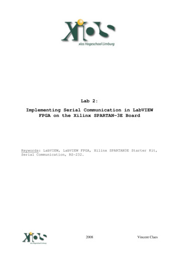
jitter and metastability in circuits, Brownian motion, atmospheric noise, nuclear decay,and random photon behavior.Because of its flexibility and fast time to market, FPGA has become a popularplatform for implementing many cryptographic systems that include TRNGs as an essential block. It is important to develop new FPGA TRNG solutions because: (i) notall hardware TRNG methods available for ASICs or other platforms are amenable toFPGA implementation; (ii) the existing FPGA TRNGs have limitations in terms ofthe throughput-per-unit-area and could be improved; and (iii) active adversarial attacksas well as variations in operational conditions such as fluctuations in temperature andvoltage supply may bias and disturb the randomness of TRNGs output bitstream. Sincemost of the state-of-the-art TRNGs operate in an open-loop fashion, it is important toincorporate a mechanism to constantly provide a feedback signal to adaptively adjustthe TRNG system parameters to increase its output bit randomness.In this work, we propose a novel technique to generate true random numbers onFPGA using the flip-flop metastability as a source of randomness. The introducedTRNG core operates within a closed-loop feedback system that actively monitors theoutput bit probabilities over windows of bit sequences and generates a proportionalfeedback signal based on any observed bias in the bit probabilities. The feedback mechanism is made possible by performing fine delay tuning using high precision PDLs withpicosecond resolution. The delay tuning ensures that the signals arrive simultaneouslyat the flip-flop to drive it into a metastable state. Our contributions are as follows.– We introduce an FPGA-based TRNG system that utilizes flip-flop metastability asthe source of randomness.– A novel feedback mechanism is introduced that performs auto-adjustment on delays in order to make the metastability condition more likely to happen.– We demonstrate the use of a PDL to perform fine tuning with a precision of higherthan a fraction of a pico-second.– Highly accurate delay measurement results for PDL are demonstrated.– The proposed TRNG system is implemented on Xilinx Virtex 5 FPGA; the hardware evaluation results demonstrate the high throughput-per-area and the high quality (i.e., true randomness) of the produced output bits.2 Related workThe work in [15] uses sampling of phase jitter in oscillator rings to generate a sequenceof random bits. The output of a group of identical ring oscillators are fed to a paritygenerator function (i.e., a multi-input XOR). The output is constantly sampled by aD-flipflop driven using the system clock. In absence of noise and identical phases, theXOR output would be constant (and deterministic). However, in presence of a phasejitter, glitches with varying non-deterministic lengths appear at the output. An implementation of this method on Xilinx Virtex II FPGAs was demonstrated in [12].Another type of TRNG is introduced in [11] that exploits the arbiter-based Physical Unclonable Function (PUF) structure. PUF provides a mapping from a set of inputchallenges to a set of output responses based on unique chip-dependent manufacturing
.Flipflop.DQ.C.ClockFig. 1: TRNG based on sampling the ring oscillator phase jitter.process variability. The arbiter-based PUF structure introduced in [3], compares the analog delay difference between two parallel timing paths. The paths are built identically,but the physical device imperfections make their timing different. A working implementation of the arbiter-based PUF was demonstrated on both ASICs [5] and FPGA [8,13]. Unlike PUFs where reliable response generation is desired, the PUF-based TRNGgoal is to generate unstable responses by driving the arbiter into the metastable state.This is essentially accomplished through violating the arbiter setup/hold time requirements. The PUF-based TRNG in [11] searches for challenges that result in small delaydifferences at the arbiter input which then cause unreliable response bits.To improve the quality of the output TRNG bitsteam and increase its randomness,various post-processing techniques are often performed. The work in [15] introducesresilient functions to filter out deterministic bits. The resilient function is implementedby a linear transformation through a generator matrix commonly used in linear codes.The hardware implementation of resilient function is demonstrated in [12] on XilinxVirtex II FPGAs. The TRNG after post processing achieves a throughput of 2Mbps using 110 ring oscillators with 3 inverters in each. A post-processing may be as simple asvon Neumann corrector [10] or may be more complicated such as an extractor function[1] or even a one-way hash function such as SHA-1 [4].Besides improving the statistical properties of the output bit sequence and removing biases in probabilities, post-processing techniques increase the TRNG resilienceagainst adversarial manipulation and variations in environmental conditions. An activeadversary may attempt to bias the output bit probabilities to reduce their entropy. Postprocessing techniques typically govern a trade-off between the quality (randomness)of the generated bit versus the throughput. Other online monitoring techniques may beused to assure a higher quality for the generated random bits. For instance, in [11],the generated bit probabilities are constantly monitored; as soon as a bias in the bit sequence is observed, the search for a new challenge vector producing unreliable responsebits is initiated. A comprehensive review of hardware TRNGs can be found in [14]. TheTRNG system proposed in this paper simultaneously provides randomness, robustness,low area overhead, and high throughput.3 Programmable delay linesProgrammable delay lines (PDLs) alter the signal propagation delay in a controlledfashion. The common mechanisms used to change the delay includes (i) varying
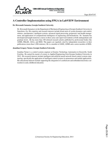
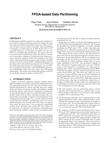
the effective load capacitance, (ii) modifying the device current drive (by increasing/decreasing the effective threshold voltage by body biasing), or (iii) incrementallyaltering the length of the signal propagation path. The first two methods are often employed in either analog fashion and/or in application specific integrated circuits (ASICs)and are not amenable to FPGA implementation.On reconfigurable digital platforms such as FPGAs, PDLs can be implemented byonly changing the signal propagation path length or by altering the circuit fanout thatmodifies the effective load capacitance. The latter is only feasible if dynamic reconfiguration is available. In other words, changing circuit fanout requires topological changesto the circuit which in turn needs a new configuration. In [2], a technique is proposedto alter the propagation path length by letting the signal bounce a few times inside theswitch matrices of FPGA instead of a direct and straight connection. The concept isillustrated in Figure 2. In the switch matrix on the left side, the signal bounces threetimes off the switch edges before it exits the switch. In the right switch, the signal onlybounces once and as a result a shorter propagation path length and a smaller delay isachieved. However, changing the switch connections points and routings require a newconfiguration, and doing so during the circuit operation is only possible by dynamicreconfigurability.Three bouncesD1DynamicallyReconfigureOne bounceD2Fig. 2: A PDL implemented by altering the signal routing inside FPGA switch matrix.In this paper, we use a novel technique to vary the signal propagation path lengthin minute increments/decrements by only using a single lookup table (LUT). The technique changes the propagation path inside the LUT. We use an example to illustratethe concept. Figure 3 shows a 3-input lookup table. The LUT consists of a set ofSRAM cells that store the intended functionality and a tree-like structure of multiplexers (MUXs) that enables selection of each individual SRAM cell content. The inputs tothe MUXs serve as an address that points to the SRAM cell whose content is selectedto appear at the output of LUT. The LUT in Figure 3 is programmed to implement aninverter, where the LUT output is always an inversion of its first input (A1 ). The otherinputs of LUT, namely A2 and A3 are functionally “don’t-cares”, but their value affectthe signal proposition path from A1 to the output. For instance, as shown in Figure3, for A2 A3 00 and A2 A3 11 the signal propagation path length (and thus thepropagation delay) from A1 to O are the shortest and the longest respectively. XilinxVirtex 5, Virtex 6, and Spartan 6 devices utilize 6-input LUTs. Therefore, by using onesingle LUT, a programmable delay inverter/buffer with five control inputs can be imple-
mented. The five inputs provide 25 32 discrete levels for controlling the delay. Themeasurement data presented in Section 6 obtained from Xilinx Virtex 5 FPGAs suggestthat the maximum delay difference from each LUT is approximately 10 pico seconds.SRAMvaluesDelay controlA1A2A3Programmabledelay inverter10A1O1A2 A30O1A10A210LUTOA33-input LUTFig. 3: Precision PDL using a single LUT.4 MetastabilityThe proposed TRNG induces metastable conditions in bi-stable logic circuit elements,i.e., flip-flops and latches. The metastable state eventually resolves to a stable state, butthe resolution process is extremely sensitive to operational conditions and circuit noise,rendering the result highly unpredictable.A ‘D’ flip-flop samples its input at the rising edge of the clock. If sampling takesplace within a narrow time window before or after the input signal transitions, a racecondition occurs. The race condition takes the flip-flop into a metastable oscillating state. The time window around the sampling moment is typically referred to assetup/hold time. The oscillation eventually settles onto a stable final state of either oneor zero. This phenomenon is demonstrated in Figure 4. Note that the probability of settling onto ‘1’ is a monotonic function of the time difference ( ) between the momentsampling happens and the moment transition occurs at the input. In fact, as shown in[16, 9, 7], the probability can be accurately modeled by a Gaussian CDF. If the delaydifference of the arriving signals is represented by and σ is proportional to the widthof the setup/hold time window, then the probability of the output being equal to one canbe written as: Prob{Out 1} Q( ),(1)σR 2where Q(x) 12π x exp( u2 )du. This model can be explained by Central LimitTheorem. Figure 4 demonstrates four scenarios for different signal arrival times. The
corresponding probabilities for the scenarios are marked by the scenario number onthe probability plot. For instance, in scenarios 1 and 4, since the delay difference islarger than the setup/hold time of the flip-flop, the output is completely deterministic.In order to obtain completely non-deterministic and unpredictable output bits with equalprobabilities (Prob{Output 1} Prob{Output 0} 0.5), our method forces the flipflop into metastability by tuning sampling and signal arrival times so they occur assimultaneously as possible (driving 0) using the PDLs.MetastableRegionSTHT1234D QProbabilityof Q 1 1210.5C4 (a)30(b) Fig. 4: (a) Flip-flop operation under four sampling scenarios, (b) probability of outputbeing equal to ‘1’ as a function of the input signals delay difference ( ). The numberson the probability plot correspond to each signal arrival scenario.5 TRNG System DesignTo drive the flip-flop into its metastable state, we use an at-speed monitor-and-controlmechanism that establishes a closed loop feedback system. The monitor module keepstrack of the output bit probabilities over repeated time intervals. It then passes on theinformation to the control unit. The control unit based on the received probability information decides to add/subtract the delay to/from top/bottom paths to calibrate the delaydifference so that it gets closer to zero. For instance, if the output bits are highly skewedtowards 1, then the delay difference ( ) must be decreased by increasing the top pathdelay to balance the probabilities. Figure 5 (a) demonstrates this concept.A straightforward implementation of the monitoring unit can be realized by usinga counter. The counter value is incremented every time the flip-flop outputs ‘1’ and isdecremented whenever the flip-flop generates a ‘0’. This is analogous to performinga running sum over the sequence of output bits where zeros are replaced by ‘ 1’. Ifzeros and ones are equally likely, the value of the counter will stay almost constant.A feedback signal is generated proportional to any deviation from this constant steadystate value. The generated error signal is fed back to the signal-to-delay transducer, i.e.,the PDL. The delay difference ( ) is updated/corrected based on the feedback signal.The described system is in effect a proportional-integral (PI) controller. The systemis depicted in Figure 5 (b). In this figure, b is the constant bias/skew in delays caused
Binary SequencePDLD QArbiter beMonitor pIntegral COut fControlG(a)(b)Fig. 5: The TRNG system model.by the routing asymmetries. p is the delay difference induced by changes in environmental and operational conditions such as temperature and supply voltage, and/or delaydifference imposed by active adversarial attacks. f is the correction feedback delaydifference injected by the PDL based on the counter value. Equation 2 expresses thetotal delay difference at the input of the flip-flop. G represents transformation carriedout by the PDL from the counter binary value to an analog delay difference. The arbiterand integrator refer to the flip-flop and counter respectively. Therefore, the followingrelationship holds; p b f .(2)An example PDL-based implementation of the TRNG system is shown in Figure 6. 21δ 2kδ.p2outputDFFp1D Q.p2 g. 6: The TRNG system implementation with a PI controller on FPGA.The PDLs are depicted as gray triangles which provide the finest and most granularlevel of control over the delays. If the resulting delay difference from one PDL is equalto δ, the effective input/output delay of a PDL, D(i), for the binary input i would be:D(i) i dc (1 i) (dc δ).(3)where dc is a constant delay value. Each programmable delay block consists of twoPDLs. The control input of top PDL inside each block is the complement of the bottomPDL control input in order to make a differential programmable delay structure. Basedon Equation 4, the differential delay is:Ddif f (i) (1 2i) δ ( 1)i δ,i 0 or 1.(4)
In this example, the programmable delay blocks are packed in groups with sizes ofmultiples of two to efficiently generate any desirable delay difference using a binarycontrol input. In other words, the first programmable delay block consists of two PDLs,the second one contains 4 PDLs, and so on. With this arrangement, the total incurreddelay difference can be written as: f G(C) KX( 1)Ci 2i δ,(5)i 0where Ci C is the ith counter bit with i 0 being the least significant bit(LSB) and i K being the most significant bit (MSB), and C represents thecounter value. δ is the smallest possible delay difference produced by one PDL.Let us assume that in the beginning the counter is resetCounter I t I b wto zero. The resulting feedback delay difference is f 111 1111 0000 4(2(K 1) 1) δ according to Equation 5. This large de110 0111 0000 3lay difference skews the output of flip-flop toward ‘1’. This101 0011 0000 2keeps raising the counter value, lowering the delay differ100 0001 0000 1ence ( ). As approaches zero, the flip-flop begins to000 0000 0001 1output ‘0’s more frequently and lowers the rate at which001 0000 0011 2the counter value was previously increasing. At the steady010 0000 0111 3state, the counter value will settle around a constant value011 0000 1111 4with a slight oscillatory behavior. Any outside perturbationon delays will cause transient fluctuations in bit probabilities; however, the automatic adjustment mechanism brings Fig. 7: Decoding operation.the system back to the equilibrium state.Although the performance of the system in Figure 6seems ideally flawless, a straightforward hardware implementation was not successful.This is because the design is based on the assumption that δs from PDLs are equal.However, due to manufacturing process variability, the δs slightly vary from one PDL toanother. As a result, it is not feasible to generate any desirable delay difference, becausethe intended weights are not exactly multiples of two anymore. In particular, the inputto the largest programmable delay block dominates the system’s output behavior.Instead, we took an alternative approach and used two sets of fine and coarse delaytuning blocks as shown in Figure 8. With n fine tuning delay lines with a resolution ofδf n , and m coarse tuning delay line with resolution of δcs , any delay difference in therange of R [nδf n mδcs , nδf n mδcs ] that satisfies Equation 6 can be produced. f wf n δf n wcs δcs(6)where wf n and wcs are integer weights (or levels) such that n wf n n and m wcs m. By carefully selecting n,m, δf n , and δcs , any delay difference with aresolution of δf n can be produced within the range R.The system in Figure 8 is designed such that the weights (or tuning levels) in Equation 6 are a function of the difference in the total number of ‘1’s at PDL inputs on the
top and bottom paths;wf n nXI t [i] nXI b [i],wcs I t [i] mXI b [i](7)i 1i 1i 1i 1mXwhere I t [i] {0, 1} and I b [i] {0, 1} are the input signals to PDLs as demonstrated inFigure 8. Thus, decoder block in Figure 8 needs to perform a mapping from the countervalue to the number of ‘1’s at PDL inputs. For example, if n 4, the counter value of‘111’ corresponds to -4 and ‘000’ corresponds to 4. Table 7 shows an example of decoding operation and corresponding tuning weights for a 3-bit counter. The conversionfrom the counter value to the effective tuning weight is expressed by Equation 8.!K 1XCi 2i , K ⌊log2 n⌋.(8)wf n ( 1)CK 1 i 0The fundamentals of the system’s operation shown in Figure 8 are the same as thesystem in Figure 6 with the only difference lying in how the feedback signal is generatedbased on the counter states.p1pnFine Tuning Blocksp2p1.It mIb2It2 Ib1I t 1 I bnIt nCIb2I t 2 I b1PostProcessingIt B BinaryMSB CounterFig. 8: The complete TRNG system.Notice that the controller type determines the response time to changes in delays aswell as the error in the steady state response. Proportional integral (PI) controllers asopposed to proportional integral derivative (PID) controller due to the lack of derivativefunction can make the system more stable in the steady state in the case of noisy data.This is because derivative action is more sensitive to higher-frequency terms in theinputs. Additionally, a PI-controlled system is less responsive to inputs (including noise)and so the system will be slower to respond to quick perturbations on the delays than awell-tuned PID system.The following two observations are important from a security standpoint. First, inthe steady state, the counter value oscillates around a constant center value (Ccenter ).Let us define the oscillation amplitude as the peak-to-peak range of the oscillations, i.e.the maximum counter value minus the minimum counter value (Cmax Cmin ). Theoscillation is not as periodic as one might think. It is rather a random walk around theoutputIbmDFFD Q.p2.Course Tuning Blockspm
center value. Each step in the random walk involves going from one counter value to aone lower or higher value:Step : Ccurrent Ccurrent 1The probability of each step (move) is a function of the current location. Intuitively theprobability of going outside the range is almost zero:Prob{Cmax Cmax 1} 0Prob{Cmin Cmin 1} 0(9)Also assuming a smooth monotonically increasing probability curve as shown inFigure 4 for the flip-flop, the farther the current counter value is from the center(Ccenter ), the lower the probability of moving farther away from the center:P rob{Ci Ci 1} P rob{Cj Cj 1} for Cj CiP rob{Ci Ci 1} P rob{Cj Cj 1} for Cj Ci(10)Each generated output bit corresponds to a counter value. The probability of theoutput being to ‘1’ is a function of the feedback counter value. The maximum countervalue almost always results in a ‘0’ output, since a ‘0’ value decrements the countervalue. Based on Equation 9, transition Cmax Cmax 1 is unlikely, thus r(Cmax )can almost never be ‘1’. The following deductions can be explained similarly:P rob{r(Ccenter ) 1} 0.5P rob{r(Cmin ) 1} 1P rob{r(Cmax ) 1} 0(11)In other words, during the random walk only those steps that pass close at the centerpoint will result in high entropy and non-deterministic responses. A smaller error inthe steady state response means oscillations happen closer to center of the probabilitytransition curve which in turn leads to higher randomness in generated output bits.In addition, it is desired that the system responds as quickly as possible to externalperturbations since the during the recovery time the TRNG generates output bits withhighly skewed probabilities.6 Experimental resultsIn this section, we present the LUT-based PDL delay measurement evaluations andTRNG hardware implementation results obtained from Xilinx Virtex 5 LX50T FPGA.Before moving onto the TRNG system performance evaluation, we shall first discuss the results of our investigation on the maximum achievable resolution of the PDLs.We set up a highly accurate delay measurement system similar to the delay characterization systems presented in [9, 7, 6].The circuit under test consists of four PDLs each implemented by a single 6-inputLUT. The delay measurement circuit as shown in Figure 9 consists of three flip-flops:
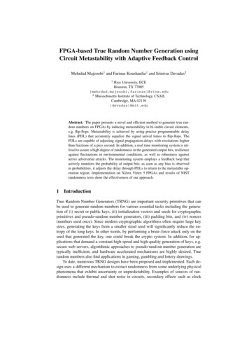
launch, sample, and capture flip-flops. At each rising edge of the clock, the launch flipflop successively sends a low-to-high and high-to-low signal through the PDLs. At thefalling edge of the clock, the output from the last PDL is sampled by the sample flipflop. At the last PDL’s output, the sampled signal is compared with the steady statesignal. If the signal has already arrived at the sample flip-flop when the sampling takesplace, then these two values will be the same; Otherwise they take on different values. Incase of inconsistency in sampled and actual values, XOR output becomes high, whichindicates a timing error. The capture flip-flop holds the XOR output for one clock cycle.To measure the absolute delays, the clock frequency is swept from a low frequencyto a high target frequency and the rate at which timing errors occur are monitored andrecorded. Timing errors start to emerge when the clock half period (T/2) approaches thedelay of the circuit under test. Around this point, the timing error rate begins to increasefrom 0% and reaches 100%. The center of this transition curve marks the point wherethe clock half period (T/2) is equal to the effective delay of the circuit under test.LaunchFlip-flopA2-6 11111A2-6 11111A2-6 11111A2-6 -6D QA2-6 11111SampleFlip-flopCaptureFlip-flopD QD QclkclkFig. 9: The delay measurement circuit. The circuit under test consists of four LUTs eachimplementing a PDL.To measure the delay difference incurred by the LUT-based PDL, the measurementis performed twice using different inputs. In the first round of measurement, the inputsto the four PDLs are fixed to A2 6 11111. In the second measurement the inputs tothe last PDL are changed to A2 6 00000. In our setup, a 32 32 array of the circuitshown on Figure 9 is implemented on a Xilinx Virtex 5 LX110 FPGA, and the delayfrom our setup is measured under the two input settings. The clock frequency is sweptlinearly from 8MHz to 20MHz using a desktop function generator and this frequencyis shifted up by 34 times inside the FPGA using the built-in PLL.The results of the measurement are shown on Figure 10. Each pixel in the imagecorresponds to one measured delay value across the array. The scale next to the colormap is in nano-seconds. Figure 10 (c) depicts the difference between the measureddelays in (a) and (b). As can be seen, the delay values in (b) are on average about 10pico-seconds larger than the corresponding pixel values in (a). This is in fact equal to theamount of delay difference caused by the coarse PDLs, i.e., δcs . The delay differenceinduced by the fine PDL of Figure 11 (a), δf n is approximately equal to 1/16 of δcs .To evaluate the performance of the TRNG system, we implement the system shownin Figure 8 using 32 coarse and fine programmable delay lines (n m 32). A 12bit counter performs the running sum operation on the output generated bits. The first
1251.10.015y1.1615yy1.16305(a) Delay for A2 6 00000301.061015x2025 0.005530(b) Delay for A2 6 111111015x202530(c) Delay differenceFig. 10: The measured delay of 32 32 circuit under tests containing a PDL with PDLcontrol inputs being set to (a) A2 6 00000 and (b) A2 6 11111 respectively. Thedifference between the delays in these two cases is shown in (c).six (LSB) bits control the finely tunable PDLs, and the next six (MSB) bits control thecoarsely tunable PDLs. Both fine and coarse PDLs are implemented by using one LUTas shown in Figure 11. As illustrated in Figure 11, to implement the fine PDL, the LUTinputs A3 to A6 are fixed to zero and the only input that controls the delay is A2 . Forthe coarse PDL, all of the LUT inputs are tied and controlled together.coioci(a) Fine PDLco654321LUT-6ciLUT-60654321io(b) Coarse PDLFig. 11: Coarse and fine PDLs implemented by a single 6-input LUT.In the first experiment, we only examine the forward system, which consists ofthe PDLs, the flip-flop, and the decoders. The tuning weights/levels are swept fromthe minimum to maximum, and the probability of the flip-flop producing a ‘1’ outputis measured at each level. This probability is measured by repeating each experimentover 100 times and counting the number of times the flip-flop outputs a ‘1’. Sincen m 32, both the fine and coarse tuning levels can go from 32 to 32. Recall thatthe tuning level represents the difference in the total number of ones at PDL inputs onthe top path minus those on the bottom path (see Equation 7). As can be observed fromFigure 12, increasing both the coarse and fine tuning levels increase the probabilityof output being equal to ‘1’. The non-smoothness of the probability curve is due tovariability in the manufacturing process which creates local non-monotonicity. Withthese observations, we expect the feedback system behavior to stabilize somewhereclose to the center of the transition point. Next, we close the feedback loop and initializethe operation. At the beginning, the counter is loaded with all ‘1’s (which results in a
10.90.8Prob{Output 1}0.70.60.50.40.3Course tune level 70.2Course tune level 80.10Course tune level 9 30 20 100Fine tune lev
Houston, TX 77005 {mehrdad.majzoobi,farinaz}@rice.edu 2 Massachusetts Institute of Technology, CSAIL Cambridge, MA 02139 {devadas}@mit.edu Abstract. The paper presents a novel and efficient method to generate tr ue ran-dom numbers on FPGAs by inducing metastability in bi-stablecircuit elements, e.g. flip-flops.