Transcription
FPGA-based Data PartitioningKaan KaraJana GicevaGustavo AlonsoSystems Group, Department of Computer ScienceETH Zürich, Tcore processors [3, 27, 32] and to explore possible hardwareacceleration [37, 41].In this paper we explore the design and implementation ofan FPGA-based data partitioning accelerator. We leveragethe flexibility of a hybrid architecture, a 2-socket machinecombining an FPGA and a CPU, to show that data partitioning can be effectively accelerated by an FPGA-baseddesign when compared to CPU-based implementations [27].The context for the work is, however, not only hybrid architectures but the increasing heterogeneity of multi-core architectures. In this heterogeneity, FPGAs are playing an increasingly relevant role both as an accelerator per se as wellas a platform for testing hardware designs that are eventually embedded in the CPU. One prominent example ofthis is Microsoft’s Catapult which uses a network of FPGAnodes in the datacenter to accelerate, e.g., page rank algorithms [28]. Other such hybrid platforms include IBM’sCAPI [34] and Intel’s research oriented experimental architecture Xeon FPGA [24]. The latter one, which we use inthis paper, brings an FPGA closer to the CPU enabling truehybrid applications where part of the program executes onthe CPU and part of it on the FPGA. Especially because ofits hybrid nature, this type of architecture enables the exploration of which CPU intensive parts of an application canbe offloaded to an FPGA as it has been done for GPUs [25].Our contributions are the following:Implementing parallel operators in multi-core machines often involves a data partitioning step that divides the datainto cache-size blocks and arranges them so to allow concurrent threads to process them in parallel. Data partitioningis expensive, in some cases up to 90% of the cost of, e.g.,a parallel hash join. In this paper we explore the use of anFPGA to accelerate data partitioning. We do so in the context of new hybrid architectures where the FPGA is locatedas a co-processor residing on a socket and with coherent access to the same memory as the CPU residing on the othersocket. Such an architecture reduces data transfer overheadsbetween the CPU and the FPGA, enabling hybrid operatorexecution where the partitioning happens on the FPGA andthe build and probe phases of a join happen on the CPU.Our experiments demonstrate that FPGA-based partitioning is significantly faster and more robust than CPU-basedpartitioning. The results open interesting options as FPGAsare gradually integrated tighter with the CPU.1.INTRODUCTIONModern in-memory analytical database engines achievehigh throughput by carefully tuning their implementation tothe underlying hardware [4,5,21]. This often involves a finegrained partitioning to cluster and split data into smallercache size blocks to improve locality and facilitate parallelprocessing. Recent work [31] has confirmed the importanceof data partitioning for joins in an analytical query context.Similar results exist for other relational operators [27]. Unfortunately, even though it improves the performance of thesubsequent processing stages (e.g., in-cache build and probefor the hash join operator), partitioning comes at a cost ofadditional passes over the data and is very heavy on randomdata access. In many cases, it can account for a significantportion of the execution time, nearly 90% [31]. Since it isan important, yet expensive sub-operator, partitioning hasbeen extensively studied to make it faster on modern multi- The hash function used for partitioning plays a crucialrole but robust hash functions are expensive [29]. In ourFPGA design we show how to use the most robust hashingavailable with no performance loss. The partitioning operation can be implemented as a fullypipelined hardware circuit, with no internal stalls or locks,capable of accepting an input and producing an output atevery clock cycle. To our knowledge this is the first FPGApartitioner to achieve this and improves throughput by1.7x over the best reported FPGA partitioner [37]. We compare our FPGA based partitioning with a stateof-the-art CPU implementation in isolation and as part ofa partitioned hash join. The experiments show that theFPGA partitioner can achieve the same performance as astate-of-the-art parallel CPU implementation, despite theFPGA having 3x less memory bandwidth and an orderof magnitude slower clock frequency. The cost model wedeveloped shows that, in future architectures without suchstructural barriers, FPGA-based partitioning will be themost efficient way to partition data.Permission to make digital or hard copies of all or part of this work for personal orclassroom use is granted without fee provided that copies are not made or distributedfor profit or commercial advantage and that copies bear this notice and the full citation on the first page. Copyrights for components of this work owned by others thanACM must be honored. Abstracting with credit is permitted. To copy otherwise, or republish, to post on servers or to redistribute to lists, requires prior specific permissionand/or a fee. Request permissions from permissions@acm.org.SIGMOD ’17, May 14–19, 2017, Chicago, Illinois, USA.c 2017 ACM. ISBN 978-1-4503-4197-4/17/05. . . 15.00DOI: http://dx.doi.org/10.1145/3035918.3035946433
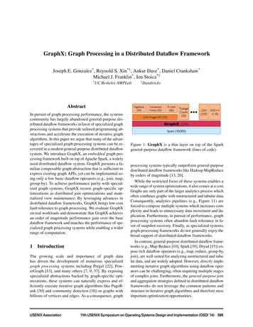
DĞŵ͘ ŽŶƚƌŽůůĞƌϲ͘ϱ ' ͬƐYW/Memory Throughput (GB/s)ΕϯϬ ' ͬƐϵϲ' DĂŝŶ DĞŵŽƌLJYW/ŶĚƉŽŝŶƚ ĂĐŚĞƐ ĐĐĞůĞƌĂƚŽƌ/ŶƚĞů yĞŽŶ Wh ůƚĞƌĂ ƚƌĂƚŝdž sFigure 1: Intel Xeon FPGA Architecture2.1XEON FPGA ARCHITECTURECPU (alone)FPGA (alone)CPU (interfered*)FPGA (interfered*)10. /09/00. .18/0.0. 27/00. .36/00. .45/00. .54/0.0. 63/00. .72/00. .81/0.90/12.30282624222018161412108642General DescriptionOur target architecture is the Intel-Altera HeterogeneousArchitecture 1 [24] (Figure 1). It consists of a dual socketwith a server grade 10-core CPU (Intel Xeon E5-2680 v2,2.8 GHz) on one socket and an FPGA (Altera Stratix V5SGXEA) on the other. The CPU and the FPGA are connected via QPI (QuickPath Interconnect). The FPGA has64B cache line and L3 cache-coherent access to the 96 GBof main memory located on the CPU socket. On the FPGA,an encrypted QPI end-point module provided by Intel handles the QPI protocol. This end-point also implements a128 KB two-way associative FPGA-local cache, using theBlock-RAM (BRAM) resources. A so-called AcceleratorFunction Unit (AFU) implemented on the FPGA can accessthe shared memory pool by issuing read and write requeststo the QPI end-point using physical addresses. Our measurements show the QPI bandwidth to be around 6.5 GB/son this platform for combined read and write channels andwith an equal amount of reads and writes. In Figure 2, acomparison of the memory bandwidth available to the CPUand the FPGA is shown, measured for varying sequentialread to random write ratios, since this is the memory accesscharacteristic that is relevant for the partitioning operation.We also show the measured bandwidth when both the CPUand the FPGA access the memory at the same time, causinga significant decrease in bandwidth for both of them.Since the QPI end-point accepts only physical addresses,the address translation from virtual to physical has to takeplace on the FPGA using a page-table. Intel also provides anextended QPI end-point which handles the address translation but comes with 2 limitations: 1) The maximum amountof memory that is allocatable is 2 GB; 2) The bandwidthprovided by the extended end-point is 20% less comparedto the standard end-point. Therefore, we choose to use thestandard end-point and implement our own fully pipelinedvirtual memory page-table out of BRAMs. We can adjustthe size of the page-table so that the entire main memorycould be addressed by the FPGA.The shared memory operation between the CPU and theFPGA works as follows: At start-up, the software application allocates the necessary amount of memory throughthe Intel provided API, consisting of 4 MB pages. It thentransmits the 32-bit physical addresses of these pages to theFPGA, which uses them to populate its local page-table.During runtime, an accelerator on the FPGA can work ona fixed size virtual address space, where the size is deter-Sequential Read/Random Write RatioFigure 2: Memory bandwidth available to the CPU andQPI bandwidth available to the FPGA depending on thesequential read to random write ratio. *The FPGA sends abalanced ratio of read/write requests (0.5/0.5) at the highestpossible rate, while the CPU read/write ratio changes asshown on the x-axis.mined by the number of 4 MB pages allocated. Any reador write access to the memory is then translated using thepage-table. The translation takes 2 clock cycles, but since itis pipelined, the throughput remains one address per clockcycle. On the CPU side, the application gets 32-bit virtualaddresses of the allocated 4 MB pages from the Intel APIand keeps them in an array. Accesses to the shared memoryare translated by a look-up into this array. The fact thata software application has to perform an additional addresstranslation step is a current drawback of the framework.However, this can very often be circumvented if most of thememory accesses by the application are sequential or if theworking set fits into a 4 MB page. We observed in our experiments that if the application is written in a consciousway to bypass the additional translation step, no overheadis visible since the translation happens rarely.2.2Effects of the Cache Coherence ProtocolBefore discussing performance in later sections, we microbenchmark the Xeon FPGA architecture. In the experiments we saw that when the CPU accesses a memory region which was lastly written by the FPGA, the memoryaccess takes significantly longer in comparison to accessinga memory region lastly written by the CPU. In the microbenchmark, we first allocate 512 MB of memory and eitherthe CPU or the FPGA fills that region with data. Then,the CPU reads the data from that region (1) sequentially,(2) randomly. The results of the single-threaded experimentis presented in Table 1. After the FPGA writes to the memory region, no matter how many times the CPU reads it, itdoes not get faster. Only after the CPU writes that sameregion do the reads become just as fast.This is a side-effect of the cache coherence protocol between two sockets connected by QPI. When the FPGA writessome cache-lines to the memory, the snooping filter on theCPU socket marks those addresses as belonging to the FPGAsocket. When the CPU accesses those addresses, they aresnooped on the FPGA socket, which causes a delay. Furthermore, the snooping filter gets only updated through writesand not reads. In a homogeneous 2-socket machine with1Following the Intel legal guidelines on publishing performance numbers we want to make the reader aware that results in this publication were generated using preproductionhardware and software, and may not reflect the performanceof production or future systems.434
Table 1: Memory access behavior depending on which sockethas lastly written to the memoryCPU reads CPU readssequentiallyrandomlyCPU writes0.1381 s1.1537 sFPGA writes0.1533 s2.4876 scache-resident buffers, each usually having the size of a cacheline, are used to accumulate a certain number of tuples, depending on the tuple size. If a buffer for a certain partitiongets full, it is written to the memory:2 CPUs, this is not an issue because both sockets wouldhave the same amount of L3 cache (in this case 25 MB).The probability of a cache-line residing in the L3 of theother socket would be very high, if that cache-line was lastwritten by that socket. However in the Xeon FPGA architecture, the FPGA has a cache of only 128 KB and anycache-line that is snooped on the FPGA socket is most likelynot found. In short, the snooping mechanism designed for ahomogeneous multi-socket architecture causes problems in aheterogeneous multi-socket architecture.This behavior particularly affects the hybrid join becauseduring the build probe phase the CPU reads regions ofmemory last written by the FPGA, when it created the partitions. During the build phase the effect is not as high,because the partitions of the build relation are read sequentially. However, during the probe phase, the build relationneeds to be accessed randomly, following the bucket chaining method from [21] and the CPU cannot prefetch data tohide the effects of the needless snooping.In our experiments, the build probe phase after the FPGApartitioning is always disadvantaged by this behavior. However, the Xeon FPGA platform is an experimental prototype, and we expect future version not to have this issue.3.3.1The size of each buffer (N) should be set so that all thebuffers fit into L1 to achieve maximum performance. Theadvantage of this technique is that it prevents frequent TLBmisses without the need of reducing the partitioning fanout. Thus, a single pass partitioning can be performed veryfast. An additional improvement to this was proposed byWassenberg et al. [38] to use non-temporal SIMD instructions for directly writing the buffers to their destinationsin the memory, bypassing the caches. That way the corresponding cache-lines do not need to be fetched and thepollution of caches is avoided. If non-temporal writes areused, N depends also on the SIMD width.Polychroniou et al. [27] and Schuhknecht et al. [32] haveboth performed extensive experimental analysis on data partitioning and confirmed that best throughput can be achievedwith the above mentioned optimizations. Accordingly, in therest of the paper we use the open-sourced implementationfrom Balkesen et al. [3] as the software baseline and use asingle-pass partitioning with software-managed buffers andnon-temporal writes enabled.CPU-BASED PARTITIONING3.2BackgroundRadix vs Hash PartitioningRichter et al. [29] describe the importance of implementing robust hash functions for analytical workloads. In particular, they have shown that for certain key distributionssimple and inexpensive radix-bit based hashing can be veryineffective in achieving a well distributed hash value space.On the other hand, robust hash functions can produce infrequently colliding and well distributed hash values for everykey distribution but they are computationally costly. Consequently, there is a trade-off between hashing robustness andperformance. To observe this trade-off in the context of datapartitioning, we perform both radix and hash partitioningon 4 different key distributions (following [29]):In a database, a data partitioner reads a relation and putstuples in their respective partitions depending on some attribute of the input key. This attribute can be determinedby either some simple calculation, e.g., taking a certain number of least significant bits of the key in the case of radixpartitioning, or something more complex, e.g., computing ahash value of the key in the case of hash partitioning. Thus,the means of determining which partition a tuple belongs tois a factor affecting the partitioning throughput.1234Code 2: Partitioning with software-managed buffersforeach tuple t in relation Ri part itio ning at trib ute ( t . key )buffers [ i ][ counts [ i ] mod N ] tcounts [ i ] if ( counts [ i ] mod N 0)copy buffers [ i ] to partitions [ i ]123456Code 1: Partitioningforeach tuple t in relation Ri pa rt it io ni n g at tr ib ut e ( t . key )partitions [ i ][ counts [ i ]] tcounts [ i ] 1. Linear Distribution: The keys are unique in the range[1:N], where N is the number of keys in the data set.2. Random Distribution: The keys are generated usingthe C pseudo-random generator in the full 32-bit integer range.Another important aspect is how the algorithm is designedto access the memory when putting the tuples into theirrespective partitions, called the shuffling phase. Since theshuffling is very heavy on random-access, the performanceis limited by TLB misses. Earlier work by Manegol et al. [21]has focused on dividing the partitioning into multiple stageswith the goal of limiting the shuffling fan-out of each stage,so that TLB misses can be minimized. Surprisingly, the multiple passes over the data required by this approach pay offin terms of performance. Later on, a more sophisticated solution proposed by Balkesen et al. [3] used software-managedcache-resident buffers, an idea first introduced for radix sortby Satish et al. [30], to improve radix partitioning. The3. Grid Distribution: Every byte of a 4B key takes avalue between 1 and 128. The least significant byteis incremented until it reaches 128, then it is reset to1. This is repeated with the next least significant byteuntil N unique keys are generated.4. Reverse Grid Distribution: The keys are generated ina similar fashion as the grid distribution. However,the incrementing starts with the most significant byte.Both grid distributions resemble address patterns andstrings.435
Throughput (Million Tuples/s)CDF(Number of Partitions)8,0006,0004,000LinearRandomGridRev. Grid2,0000016,38432,76865,536Number of Tuples/PartitionCDF(Number of Partitions)(a) Radix partitioning is applied.400300Radix Part.(linear)200Radix Part.(random)Radix Part.(grid)Radix part.(rev. grid)100Hash Part.(all)8,0001248106,000Number of Threads4,000Figure 4: CPU Partitioning throughput with 8B tuples, forvarying key distributions and partitioning methods. Hashpartitioning delivers for every key distribution the samethroughput.LinearRandomGridRev. Grid2,0000016,38432,76865,536Number of Tuples/Partitiondetails about the implementation and various optimizations are discussed in Section 3.1.2. For each partition, a build and probe phase follows:(b) Hash partitioning is applied.Figure 3: The distribution of tuples across 8192 partitionsrepresented as a cumulative distribution function.(a) During the build phase, a cache resident hash table is built from a partition of R.(b) During the probe phase, the tuples of the corresponding partition of S are scanned and for eachone, the hash table is probed to find a match.When radix partitioning is used, the resulting partitionsmay have unbalanced distributions as depicted in Figure 3a.On the other hand, if hash partitioning is used with a robust hash function, such as murmur hashing [2], the createdpartitions have approximately the same number of tuples asshown in Figure 3b.Although hash partitioning is robust against various keydistributions, using a powerful hash function lowers the partitioning throughput as depicted in Figure 4. However, asthe number of threads is increased, the partitioning process becomes memory bound. Consequently, there are freeclock cycles available as the CPU waits on memory requests.These free clock cycles can be used for calculating a morepowerful hash function. Thus, the throughput slowdownobserved with few threads disappears.3.35004.FPGA-BASED PARTITIONINGIn this section we give a detailed description of the VHDLimplementation of the FPGA partitioner. Because the accelerators on the Xeon FPGA architecture access the memory in 64B cache-line granularity, the partitioner circuit isdesigned to work on that data width. The design is fullypipelined requiring no internal stalls or locking mechanismsregardless of input type. Therefore, the partitioner circuitis able to consume and produce a cache-line at every clockcycle.When it comes to tuple width, the design supports various tuple sizes (e.g., 8B, 16B, 32B and 64B). Throughoutthe first parts of this section, we explain the partitioner architecture in the 8B tuple configuration, since this is thesmallest granularity we are able to achieve and poses thelargest challenge for write combining. Besides, 8B tuples 4B key, 4B payload are a common scheme in most of theprevious work [4, 31] and that allows for direct comparisonsafterwards in the evaluation. We later show how to changethe design to work on larger tuples and how this considerablyreduces resource consumption on the FPGA. Additionally,the partitioner has multiple modes of operation for accommodating both column and row store memory layouts, andfor handling data with large amounts of skew, as explainedin Section 4.5.Partitioned Hash JoinThe relational equi-join is a primary component of almostall analytical workloads and constitutes a significant portionof the execution time of a query. Therefore, it has received alot of attention in terms of how to improve its performanceon modern architectures. A recent paper by Schuh et al. [31]provides a detailed analysis of implementations and optimizations for both hash- and sort-based joins published inthe last few years [3, 4, 8, 19, 20]. The conclusion is that partitioned, hardware-conscious, radix hash-joins have a clearperformance advantage over non-partitioned and sort-basedjoins on modern multi-core architectures for large and nonskewed relations. Hence, in the rest of this paper we evaluatehow offloading the partitioning phase to a hardware accelerator affects the performance of radix hash join algorithm.The partitioned hash join algorithm (also known as radixjoin) operates in several stages:4.1Hash Function ModuleFigure 5 shows the top level design of the circuit. Every tuple in a received cache-line first passes through a hashfunction module, which can be configured to do either murmur hashing [2] or a radix-bit operation taking N least sig-1. Both relations (R and S) are partitioned using radixpartitioning, so that each partition fits into cache. More436
dƵƉůĞ ϳ͗ϰ ŬĞLJϰ ǀĂůƵĞ&ƌŽŵ YW/ ĂĐŚĞ ŝŶĞdƵƉůĞ ϭ͗ dƵƉůĞ Ϭ͗ϰ ŬĞLJ ϰ ŬĞLJϰ ǀĂůƵĞ ϰ �ĐƚŝŽŶ &ƵŶĐƚŝŽŶE ďŝƚƐ ŚĂƐŚ н ϴ ƚƵƉůĞ&/&K ϳ&/&K ϭ&/&K ϬtƌŝƚĞ Žŵď͘ϭtƌŝƚĞ Žŵď͘ϬE ďŝƚƐ ŚĂƐŚ н ϴ ƚƵƉůĞtƌŝƚĞ Žŵď͘ϳZĞĂĚ ĨƌŽŵ &/&KǁƌŝƚĞϮϬϬ D,njϴ ƚƵƉůĞ Z D ĂĚĚƌĞƐƐ с ŚĂƐŚ Z D ĚĂƚĂ с ƚƵƉůĞ&ŝůů ZĂƚĞ Z D Z D ϳ Z D ϭ Z D Ϭ&ŝůů ƌĂƚĞ WĂƌƚ͘ ϭdƵƉůĞ ŝŶ WĂƌƚ͘ ϭdƵƉůĞ ŝŶ WĂƌƚ͘ ϭdƵƉůĞ ŝŶ WĂƌƚ͘ ϭ&ŝůů ƌĂƚĞ WĂƌƚ͘ ϮdƵƉůĞ ŝŶ WĂƌƚ͘ ϮdƵƉůĞ ŝŶ WĂƌƚ͘ ϮdƵƉůĞ ŝŶ WĂƌƚ͘ Ϯ&ŝůů ƌĂƚĞ WĂƌƚ͘ EdƵƉůĞ ŝŶ WĂƌƚ͘ EdƵƉůĞ ŝŶ WĂƌƚ͘ EdƵƉůĞ ŝŶ WĂƌƚ͘ EƌĞĂĚ/ĨĨŝůů ƌĂƚĞŝƐ ϴŶŽƚŝĨLJZĞĂĚ ĨƌŽŵ Z DE ďŝƚƐ ŚĂƐŚ н ϴΎϴ ƚƵƉůĞ&/&K tƌŝƚĞ ĂĐŬ,ŝƐƚŽŐƌĂŵ Z DZĞĂĚ ĨƌŽŵ &/&K ŽƵŶƚ WĂƌƚ͘ ϭ ŽƵŶƚ WĂƌƚ͘ Ϯ ĂĐŚĞ ůŝŶĞ ƚŽ ƐĞŶĚ͗ E ďŝƚ ŚĂƐŚ ĂŶĚ ϴ dƵƉůĞƐ ĂĐŚĞ ůŝŶĞ ƚŽ ƐĞŶĚ͗ E ďŝƚ ŚĂƐŚ ĂŶĚ ϴ dƵƉůĞƐ ĂĐŚĞ ůŝŶĞ ƚŽ ƐĞŶĚ͗ E ďŝƚ ŚĂƐŚ ĂŶĚ ϴ dƵƉůĞƐKĨĨƐĞƚ ƌĂŵ ŽƵŶƚ WĂƌƚ͘ ϭ ŽƵŶƚ WĂƌƚ͘ Ϯ&/&K ŽƵŶƚ WĂƌƚ͘ E ĂĐŚĞ ůŝŶĞ ƚŽ ƐĞŶĚ͗ ϯϮ ďŝƚ ĚĚƌĞƐƐ ĂŶĚ ϴ dƵƉůĞƐ ĂĐŚĞ ůŝŶĞ ƚŽ ƐĞŶĚ͗ ϯϮ ďŝƚ ĚĚƌĞƐƐ ĂŶĚ ϴ dƵƉůĞƐ ĂĐŚĞ ůŝŶĞ ƚŽ ƐĞŶĚ͗ ϯϮ ďŝƚ ĚĚƌĞƐƐ ĂŶĚ ϴ dƵƉůĞƐFigure 6: Design of the write combiner module for 8B tuples. ŽƵŶƚ WĂƌƚ͘ EdŽ YW/Figure 5: Top level design of the hardware partitioner for8B tuples.nificant bits of the key. The important thing to keep inmind is that in the synthesized hardware for the pseudocode in Code 3, every calculation (Lines 6-11) is a stage of apipeline, which is very different from a sequential executionpoint-of-view of software. For example, when Line 9 executes the multiplication on the first received key, Line 8 canexecute the bit-shift on the second received key and so on.Therefore, the hash function module can produce an outputat every clock cycle, regardless of how many intermediatestages are inserted into the calculation pipeline. The onlything that increases with additional pipeline stages is thelatency. For murmur hashing the latency is 5 clock cycles:(1/200M Hz) · 5 25ns.Code 3: Hash Function Module for 4B keys. Pseudo-Codefor VHDL, where each line is always active.1 Input is:264 - bit tuple key , payload 3 Output is:4N - bit hash & 64 - bit tuple key , payload 5 if ( do hash 1)6key key 16;7key * 0 x85ebca6b ;8key key 13;9key * 0 xc2b2ae35 ;10key key 16;11hash N LSBs of key ;12 else13hash N LSBs of key ;4.2Write Combiner ModuleThe output of every hash function module is placed intoa first-in, first-out buffer (FIFO), waiting to be read by awrite combiner module. The job of the write combiner is toput 8 tuples belonging to the same partition together in a437cache-line before they are written back to the memory. Todemonstrate the benefits of write combining, consider thecase when no write combiner is used: For every tuple goinginto a partition first its corresponding cache-line from thememory has to be fetched (64B read). Then, the tuple is inserted into the cache-line at a certain offset and written backto memory (64B write). This operation takes place for every tuple entering the partitioner, say T tuples. In total, theamount of memory transfers excluding the initial sequentialread of tuples is (64 64) · T Bytes. With write combiningenabled we have to write approximately as much data as wehave read: 64 · T /8 Bytes, a 16x improvement over the nowrite combining option. Since the hardware partitioner inthe current architecture is already bound by memory bandwidth, we choose to implement a fully-pipelined write combiner to achieve the best performance on the current platform.Here we describe in more detail how the circuit avoidsinternal locking in the write combiner module. The modulereads a tuple from its input FIFO as soon as it sees that theFIFO is not empty. It then reads from an internal BRAMthe fill rate of the partition, to which the tuple belongs.The fill rate holds a value between 0 and 7 (the number ofpreviously received tuples belonging to the same partition),specifying into which BRAM the tuple should be put (seeFigure 6). Reading the fill rate from the BRAM takes 2clock cycles. However, during this time the pipeline doesnot need to be stalled since the BRAM can output a valueat every clock cycle. The design challenge here is inserting aforwarding register outside the BRAMs, to handle the caseswhere a read and a write occur to the same address at thesame clock cycle. Basically, a comparison logic recognizes ifthe current tuple goes into the same partition as one of theprevious 2 tuples (Lines 6 and 8 in Code 4). If that is thecase, the issued read of the fill rate 2 cycles ago is ignored andthe in-flight fill-rate of either one of the matching hashes isforwarded (Lines 7 or 9 in Code 4). Otherwise, the requestedfill rate is read to determine which BRAM the tuple belongsto. If the fill rate for any partition reaches 7, it is firstreset to 0, the tuple is written to the last BRAM, and then
a read from the corresponding addresses of all 8 BRAMsis requested. The actual read from the BRAMs happens1 clock cycle later, since the BRAMs operate with 1 cyclelatency. During the read cycle, if a write occurs to the sameaddress as the read, there is no problem because of this 1clock cycle latency. No data gets lost and no pipeline stallsare incurred regardless of any input pattern.ϴ dƵƉůĞƐϴ ϴ dƵƉůĞ dƵƉůĞϮϬϬ D,nj,ĂƐŚ&ƵŶĐ͘Code 4: Write Combiner Module. 1d and 2d represent thesame signals after 1 and 2 clock cycles, respectively. PseudoCode for VHDL, where each line is always active.1 Input is:2N - bit hash & 64 - bit tuple3 Output is:4N - bit hash & 512 - bit combined tuple56 if ( hash hash 1d )7which BRAM which BRAM 1d 1;8 else if ( hash hash 2d )9which BRAM which BRAM 2d 1;10 else11which BRAM fill rate [ hash ];1213 if ( which BRAM 7)14fill rate [ hash ] 0;15read from BRAM True ;16 else17fill rate [ hash ] ;1819 BRAM [ which BRAM ][ hash ] tuple ;20 if ( read from BRAM 2d True )21combined tuple BRAM [7][ hash 1d ] &22BRAM [6][ hash 1d ] & .23BRAM [0][ hash 1d ];At the end of a partitioning run, some partitions in thewrite combiner BRAMs may remain empty. In fact, thishappens almost every time since the scattering of tuples to8 write combiners are irregular and some cache-lines remainpartially filled in the end. To write back every tuple a flushis performed, where every address of the BRAMs is read sequentially and full cache-lines are put into the output FIFO.To obtain a full cache-line in this case, the empty slots arefilled with dummy keys, which later on won’t be regarded bythe software application. Because of this non-perfect gathering after the scattering, the partitioner circuit writes somemore data than it receives. In the worst case, every partitionin a write combiner module would be filled with one singletuple, making the other 7 tuples at every partition a dummykey. This overhead is in principle no different than the oneincurred through aligning and padding to enable the use ofSIMD or optimize cache accesses on a CPU.4.3 ĂĐŚĞ ŝŶĞ &ƌŽŵ YW/ϴ dƵƉůĞ,ĂƐŚ ,ĂƐŚ&ƵŶĐ͘ &ƵŶĐ͘&/&K ϳ&/&K ϭ &/&K ϬtƌŝƚĞ Žŵď͘ϳtƌŝƚĞ tƌŝƚĞ Žŵď͘ Žŵď͘ϭϬǁƌŝƚĞ&ŝůů ZĂƚĞ Z DƌĞĂĚZĞĂĚ ĨƌŽŵ &/&K Z D ϳ Z D Z D ϭϬ/ĨĨŝůů ƌĂƚĞŝƐ ϴŶŽƚŝĨLJZĞĂĚ ĨƌŽŵ Z D&/&K tƌŝƚĞ ĂĐŬdŽ YW/ϭϲ dƵƉůĞƐ ĂĐŚĞ ŝŶĞ &ƌŽŵ YW/ϭϲ dƵƉůĞϭϲ �ŶϮϬϬ D,nj&/&K ϯ&/&K ϬtƌŝƚĞ ŽŵďŝŶĞƌϯtƌŝƚĞ ŽŵďŝŶĞƌϬǁƌŝƚĞZĞĂĚ ĨƌŽŵ &/&K&ŝůů ZĂƚĞ Z D Z D ϯ Z D Ϯ Z D ϭ Z D ϬƌĞĂĚ/ĨĨŝůů ƌĂƚĞŝƐ ϰŶŽƚŝĨLJZĞĂĚ ĨƌŽŵ Z D&/&K tƌŝƚĞ ĂĐŬdŽ YW/ϯϮ dƵƉůĞƐ ĂĐŚĞ ŝŶĞ &ƌŽŵ YW/ϯϮ dƵƉůĞϯϮ �ŶϮϬϬ D,nj&/&K ϭ&/&K ϬtƌŝƚĞ ŽŵďŝŶĞƌϭtƌŝƚĞ ŽŵďŝŶĞƌϬǁƌŝƚĞZĞĂĚ ĨƌŽŵ &/&K&ŝůů ZĂƚĞ Z D Z D ϭƌĞĂĚ Z D Ϭ/ĨĨŝůů ƌĂƚĞŝƐ ϮŶŽƚŝĨLJZĞĂĚ ĨƌŽŵ Z D&/&K tƌŝƚĞ ĂĐŬdŽ YW/ϲϰ dƵƉůĞƐ ĂĐŚĞ ŝŶĞ &ƌŽŵ YW/ϲϰ dƵƉůĞϮϬϬ D,nj,ĂƐŚ&ƵŶĐƚŝŽŶ&/&K ϬtƌŝƚĞ ŽŵďŝŶĞƌϬǁƌŝƚĞZĞĂĚ ĨƌŽŵ &/&K&ŝůů ZĂƚĞ Z D Z D ϬƌĞĂĚ/ĨĨŝůů ƌĂƚĞŝƐ ϭŶŽƚŝĨLJZĞĂĚ ĨƌŽŵ Z D&/&K tƌŝƚĞ ĂĐŬdŽ YW/Figure 7: Changes to the design to support wider tuples.tain the end address of a current cache-line, which can thenbe sent. For maintaining the integrity of the offset BRAM,the forwarding logic described in Section 4.2 is used.The circuit is able to produce a cache-line at every clockcycle when the entire pipeline is filled, but the QPI bandwidth cannot handle this and puts back-pressure on thewrite back module. This back-pressure has to be propagated along the pipeline to ensure that no FIFO experiencesan overflow, which would cause data to be lost. We handlethis by issuing only so many read requests as there are freeslots in the first stage FIFOs just after the hash functionmodules (see Figure 5). If the QPI write bandwidth wouldbe more than 12.8 GB/s, which is the output th
comparison of the memory bandwidth available to the CPU and the FPGA is shown, measured for varying sequential read to random write ratios, since this is the memory access characteristic that is relevant for the partitioning operation. We also show the measured bandwidth when both the CPU and the FPGA access the memory at the same time, causing