Transcription
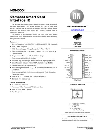
NCN6001Compact Smart CardInterface ICThe NCN6001 is an integrated circuit dedicated to the smart cardinterface applications. The device handles any type of smart cardthrough a simple and flexible microcontroller interface. On top of that,thanks to the built in chip select pin, several couplers can beconnected in parallel.The device is particularly suited for low cost, low powerapplications, with high extended battery life coming from extremelylow quiescent current.www.onsemi.com1TSSOP 20DTB SUFFIXCASE 948EFeatures 100% Compatible with ISO 7816 3, EMV and GIE CB StandardsFully GSM CompliantWide Battery Supply Voltage Range: 2.7 VCC 5.5 VProgrammable CRD VCC Supply Handles 1.8 V, 3.0 V or 5.0 VCard OperationProgrammable Rise and Fall Card Clock SlopesProgrammable Card Clock DividerBuilt in Chip Select Logic Allows Parallel Coupling OperationESD Protection on Card Pins (8.0 kV, Human Body Model)Supports up to 40 MHz Input ClockBuilt in Programmable CRD CLK Stop Function Handles Run orLow StateProgrammable CRD CLK Slopes to Cope with Wide OperatingFrequency RangeFast CRD VCC Turn on and Turn off SequenceThese are Pb Free DevicesPIN CONNECTIONSI/O 120 CRD IOINT 219 CRD RSTCLK IN 318 CRD DETMOSI 417 CRD CLKCLK SPI 516 GNDEN RPU 615 C4/S0MISO 714 C8/S1CS 813 CRD VCCVCC 912 Lout HLout L 1011 PWR GND(Top View)Typical Applications E Commerce InterfaceAutomatic Teller Machine (ATM) Smart CardPoint of Sales (POS) SystemPay TV SystemMARKING DIAGRAM20NCN6001ALYWGG1ALYWG Assembly Location Wafer Lot Year Work Week Pb Free Package(Note: Microdot may be in either location)ORDERING INFORMATIONSee detailed ordering and shipping information in the packagedimensions section on page 32 of this data sheet. Semiconductor Components Industries, LLC, 2014October, 2014 Rev. 61Publication Order Number:NCN6001/D
NCN6001VCCJ19GND12U1CRD DETVCCCRD IOI/OCRD RSTINTMICROCONTROLLER345786R147 k10CLK INCRD CLKCRD VCCMOSICLK SPIC4/S0MISOC8/S1GNDCSEN RPULout LVCC1820719217313515GND1144168C210 F11PWR GNDLout HNCN6001GND18SwaSwbI/ORSTCLKGNDISO781610 FC117VCCC4C8SMARTCARD C12L1GNDGND22 HFigure 1. Typical ApplicationVCCPROGRAMMABLECARD DETECTION50 kINT2CS8INTERRUPT BLOCK18 CRD DET500 kVCCMOSI4CLK SPI59DC/DC CONVERTER3 StatesADDRESS DECODING7DUAL 8 BITSHIFT REGISTERMISOb7b6b5b4b3b2b1b0b0b1VCC10 Lout L12 Lout H13 CRD VCC11 PWR GNDEN RPU6I/OCLOCKDIVIDER20 k1b5b6b415 C4/S0CARD PINS DRIVER3ISO7816 SEQUENCERCLK INb2b3LOGIC CONTROLb7GND14 C8/S119 CRD RST17 CRD CLK20 CRD IO20 kGROUND16CRD VCCGNDFigure 2. Block Diagramhttp://onsemi.com2
NCN6001PIN FUNCTIONS AND tPullup2INTOUTPUTPullupThis pin is activated LOW when a card has been inserted and detected by CRD DET pin.Similarly, an interrupt is generated when the CRD VCC output is overloaded, or when the cardhas been extracted whatever be the transaction status (running or standby).The INT signal is reset to High according to Table 7 and Figure 10. On the other hand, the pinis forced to a logic High when the input voltage VCC drops below 2.0 V.3CLK INCLOCKINPUTHighimpedanceThe built in Schmitt trigger receiver makes this pin suitable for a large type of clock signal(Figure 29). This pin can be connected to either the microcontroller master clock, or to acrystal signal, to drive the external smart cards. The signal is fed to the internal clock selectorcircuit and translated to the CRD CLK pin at either the same frequency, or divided by 2 or 4,depending upon the programming mode.Note: The chip guarantees the EMV 50% Duty Cycle when the clock divider ratio is 1/2 or 1/4,even when the CLK IN signal is out of the 45% to 55% range specified by ISO and EMVspecifications.Care must be observed, at PCB level, to minimize the pick up noise coming from the CLK INline.4MOSIINPUTMaster Out Slave In: SPI Data Input from the external microcontroller. This byte contents theaddress of the selected chip among the four possible, together with the programming code fora given interface.5CLK SPIINPUTClock Signal to synchronize the SPI data transfer. The built in Schmitt trigger receiver makesthis pin compatible with a wide range of input clock signal (Figure 29). This clock is fullyindependent from the CLK IN signal and does not play any role with the data transaction.6EN RPUINPUT, Logic7MISOOUTPUT8CSINPUTThis pin synchronizes the SPI communication and provides the chip address and selectedfunctions.All the NCN6001 functions, both programming and card transaction, are disabled whenCS H.9VCCPOWERThis pin is connected to the NCN6001 supply voltage and must be bypassed to ground bya 10 F/6.0 V capacitor.Since tantalum capacitors have relative high ESR, using low ESR ceramic type (MURATAX5R, Resr 100 m ) is highly recommended.10Lout LPOWERThe Low Side of the external inductor is connected between this pin and pin 12 to provide theDC/DC function. The current flowing into this inductor is internally sensed and no externalshunt resistor is used. Typically, Lout 22 H, with DSR 2.0 , yields a good efficiencyperformance for a maximum 65 mA DC output load.Note: The inductor shall be sized to handle the 450 mA peak current flowing during the DC/DCoperation (see CoilCraft manufacturer data sheet).This pin is connected to an external microcontroller interface. A bidirectional level translatoradapts the serial I/O signal between the smart card and the microcontroller. The leveltranslator is enabled when CS L, the sub address has been selected and the systemoperates in the Asynchronous mode. When a Synchronous card is in use, this pin isdisconnected and the data and the transaction take place with the MISO b3 register.The internal pullup resistor connected on the C side is activated and visible by the selectedchip only.This pin is used to activate the I/O internal pullup resistor according to the here below truetable:EN RPU Low I/O Pullup resistor disconnectedEN RPU High I/O Pullup resistor connectedWhen two or more NCN6001 chips shares the same I/O bus, one chip only shall have theinternal pullup resistor enabled to avoid any overload of the I/O line.Moreover, when Asynchronous and Synchronous cards are handled by the interfaces, theactivated I/O pullup resistor must preferably be the one associated with the Asynchronouscircuit.On the other hand, since no internal pullup bias resistor is built in the chip, pin 6 must beconnected to the right voltage level to make sure the logic function is satisfied.Master In Slave Out: SPI Data Output from the NCN6001. This byte carries the state of theinterface, the serial transfer being achieved according to the programmed mode (Table 2),using the same CLK SPI signal and during the same MOSI time frame. The three high bits[b7:b5] have no meaning and shall be discarded by the microcontroller. An external 4.7 k Pulldown resistor might be necessary to avoid misunderstanding of the pin 7 voltage during theHigh Z state.http://onsemi.com3
NCN6001PIN FUNCTIONS AND DESCRIPTION (continued)TSSOPNameType11PWR GNDPOWERThis pin is the Power Ground associated with the built in DC/DC converter and must beconnected to the system ground together with GROUND pin 16. Using good quality groundplane is recommended to avoid spikes on the logic signal lines.Description12Lout HPOWERThe High Side of the external inductor is connected between this pin and pin 10 to activate theDC/DC function. The built in NMOS and PMOS devices provide the switching functiontogether with the CRD VCC voltage rectification (Figure 16).13CRD VCCPOWERThis pin provides the power to the external card. It is the logic level “1” for CRD IO,CRD RST, CRD C4, CRD C8 and CRD CLK signals.The energy stored by the DC/DC external inductor Lout must be smoothed by a 10 F/LowESR capacitor, connected across CRD VCC and GND. Using ceramic type of capacitor(MURATA X5R, ESR 50 m ) is strongly recommended. In the event of a CRD VCC UVLOWvoltage, the NCN6001 detects the situation and feedback the information in the STATUS bit.The device does not take any further action, particularly the DC/DC converter is neitherstopped nor re programmed by the NCN6001. It is up to the external MPU to handle thesituation.However, when the CRD VCC is overloaded, the NCN6001 shuts off the DC/DC converter,runs a Power Down ISO sequence and reports the fault in the STATUS register.Since high transient current flows from this pin to the load, care must be observed, at PCBlevel, to minimize the series ESR and ESL parasitic values. The NCN6001 demo boardprovides an example of a preferred PCB layout.14C8/S1I/OAuxiliary mixed analog/digital line to handle either a synchronous card, or as Chip SelectIdentification (MISO, Bit 0): see Figure 8. The pin is driven by an open drain stage, the pullupresistor being connected to the CRD VCC supply. When the pin is used as a logic input(asynchronous cards), the positive logic condition applies:Connected to GND Logic ZeroConnected to VCC or left Open Logic OneA built in accelerator circuit makes sure the output positive going rise time is fully within theISO/EMV specifications.NOTE:15C4/S0I/OThe pin is capable of reading the logic level when the chip operates an asynchronousinterface, but is not intended to read the data from the external card when operated inthe synchronous mode. It merely returns the logic state forced during a writeinstruction to the card.Auxiliary mixed analog/digital line to handle either a synchronous card, or as Chip SelectIdentification (MISO, Bit 1): see Figure 8. The pin is driven by an open drain stage, the pullupresistor being connected to the CRD VCC supply. When the pin is used as a logic input(asynchronous cards), the positive logic condition applies:Connected to GND Logic ZeroConnected to VCC or left Open Logic OneA built in accelerator circuit makes sure the output positive going rise time is fully within theISO/EMV specifications.NOTE:The pin is capable of reading the logic level when the chip operates an asynchronousinterface, but is not intended to read the data from the external card when operated inthe synchronous mode. It merely returns the logic state forced during a writeinstruction to the card.16GNDSIGNALThe logic and low level analog signals shall be connected to this ground pin. This pin must beexternally connected to the PWR GND pin 12. The designer must make sure no high currenttransients are shared with the low signal currents flowing into this pin.17CRD CLKOUTPUTThis pin is connected to the CLK pin of the card connector. The CRD CLK signal comes fromthe clock selector circuit output. An internal active pull down NMOS device forces this pin toGround during either the CRD VCC startup sequence, or when CRD VCC 0 V.The rise and fall slopes, either FAST or SLOW, of this signal can be programmed by the MOSImessage (Table 2).Care must be observed, at PCB level, to minimize the pick up noise coming from theCRD CLK line.http://onsemi.com4
NCN6001PIN FUNCTIONS AND DESCRIPTION (continued)TSSOPNameTypeDescription18CRD DETINPUTThe signal coming from the external card connector is used to detect the presence of the card.A built in pullup low current source biases this pin High, making it active LOW, assuming oneside of the external switch is connected to ground. A built in digital filter protect the systemagainst voltage spikes present on this pin.The polarity of the signal is programmable by the MOSI message, according to the logic statedepicted Table 2. On the other hand, the meaning of the feedback message contained in theMISO register bit b4, depends upon the SPI mode of operation as defined here below:SPI Normal Mode: The MISO bit b4 is High when a card is inserted, whatever be the polarityof the card detect switch.SPI Special Mode: The MISO bit b4 copies the logic state of the Card detect switch asdepicted here below, whatever be the polarity of the switch used to handle the detection:CRD DET Low MISO/b4 LowCRD DET High MISO/b4 HighIn both cases, the chip must be programmed to control the right logic state (Table 2).Since the bias current supplied by the chip is very low, typically 5.0 A, care must be observedto avoid low impedance or cross coupling when this pin is in the Open state.19CRD RSTOUTPUTThis pin is connected to the RESET pin of the card connector. A level translator adapts theRESET signal from the microcontroller to the external card. The output current is internallylimited to 15 mA.The CRD RST is validated when CS Low and hard wired to Ground when the card isdeactivated, by and internal active pull down circuit.Care must be observed, at PCB design level, to avoid cross coupling between this signal andthe CRD CLK clock.20CRD IOI/OPullupThis pin handles the connection to the serial I/O pin of the card connector. A bidirectional leveltranslator adapts the serial I/O signal between the card and the microcontroller. An internalactive pull down MOS device forces this pin to Ground during either the CRD VCC startupsequence, or when CRD VCC 0 V. The CRD IO pin current is internally limited to 15 mA.Care must be observed, at PCB design level, to avoid cross coupling between this signal andthe CRD CLK clock.http://onsemi.com5
NCN6001MAXIMUM RATINGS (TA 25 C unless otherwise noted)SymbolValueUnitPower Supply VoltageRatingVCC6.0VPower Supply CurrentNote: This current represents the maximum peak current thepin can sustain, not the NCN6001 average consumption.Ibat500mAPower Supply CurrentICC150 (Internally Limited)mADigital Input PinsVin 0.5 V Vin VCC 0.5 V, but 6.0 VVDigital Input PinsIin 5.0mADigital Output PinsVout 0.5 V Vin VCC 0.5 V, but 6.0 VVDigital Output PinsIout 10mACard Interface PinsVcard 0.5 V Vcard CRD VCC 0.5 VVCard Interface Pins, excepted CRD CLKIcard15 (Internally Limited)mAInductor CurrentILout500 (Internally Limited)mAESD Capability (Note 1)Standard PinsCard Interface PinsCRD DETVESD2.08.04.0kVkVkVPower Dissipation @ Tamb 85 CThermal Resistance, Junction to Air (R JA)PDSR JA320125mW C/WOperating Ambient Temperature RangeTA 25 to 85 COperating Junction Temperature RangeTJ 25 to 125 CTJmax 150 CTstg 65 to 150 CMaximum Junction Temperature (Note 2)Storage Temperature RangeStresses exceeding those listed in the Maximum Ratings table may damage the device. If any of these limits are exceeded, device functionalityshould not be assumed, damage may occur and reliability may be affected.1. Human Body Model, R 1500 , C 100 pF.2. Absolute Maximum Rating beyond which damage to the device may occur.http://onsemi.com6
NCN6001DIGITAL PARAMETERS @ 2.7 V VCC 5.5 V ( 25 C to 85 C ambient temperature, unless otherwise noted).Note: Digital inputs undershoot 0.3 V to ground, Digital inputs overshoot 0.3 V to VCC.PinSymbolMinTypMaxInput Asynchronous Clock Duty Cycle 50%@ VCC 3.0 V Over the Temperature Range@ VCC 5.0 V Over the Temperature Range3FCLKIN 3040Input Clock Rise TimeInput Clock Fall Time3FtrFtf2.52.5 nsnsInput SPI Clock5FCLKSPI 15MHzInput CLK SPI Rise/Fall Time @ Cout 30 pF5trspi, tfspi 12nsInput MOSI Rise/Fall Time @ Cout 30 pF4trmosi,tfmosi 12nsOutput MISO Rise/Fall Time @ Cout 30 pF7trmiso,tfmiso 12nsInput CS Rise/Fall Time8trstr, tfstr 12nstRIOtFIO 0.80.8 s s205080k 0.70 * VCC VCC0 0.3 * VCCVCC 1.0 V VCC 0.433 RatingI/O Data Transfer Switching Time, both directions(I/O and CRD IO), @ Cout 30 pFI/O Rise Time * (Note 4)I/O Fall TimeINT Pullup ResistanceMHz1, 202RITAPositive Going Input High Voltage Threshold(CLK IN, MOSI, CLK SPI, EN RPU, CS)2, 3, 4, 5,6, 8VIANegative Going Input High Voltage Threshold(CLK IN, MOSI, CLK SPI, EN RPU, CS)2, 3, 4, 5,6, 8VILLAOutput High VoltageINT, MISO @ OH 10 A2, 7VOHOutput Low VoltageINT, MISO @ OH 200 A2, 7Delay Between Two Consecutive CLK SPI SequenceUnit5VVVVOLtdclkVnsProduct parametric performance is indicated in the Electrical Characteristics for the listed test conditions, unless otherwise noted. Productperformance may not be indicated by the Electrical Characteristics if operated under different conditions.3. Since a 20 k (typical) pullup resistor is provided by the NCN6001, the external MPU can use an Open Drain connection. On the other hand,NMOS smart cards can be used straightforward.http://onsemi.com7
NCN6001POWER SUPPLY @ 2.7 V VCC 5.5 V ( 25 C to 85 C ambient temperature, unless otherwise noted).PinSymbolMinTypMaxUnitInput Power SupplyRating9VCC2.70 5.50VVStandby Supply Current Conditions:INT CLK IN CLK SPI CS HI/O MOSI EN RPU H, No Card InsertedVCC 3.0 VVCC 5.0 V9ICCsbDC Operating CurrentCLK IN Low, All Card Pins Unloaded@ VCC 3.3 V, CRD VCC 5.0 V@ VCC 5.5 V, CRD VCC 5.0 V9VCC Under Voltage DetectionHighVCC Under Voltage DetectionLowVCC Under Voltage (Note 6)9Output Card Supply Voltage@ 2.7 V VCC 5.5 VCRD VCC 1.8 V @ Iload 35 mACRD VCC 3.0 V @ Iload 60 mACRD VCC 5.0 V @ Iload 65 mA13Maximum Continuous Output Current@ CRD VCC 1.8 V@ CRD VCC 3.0 V@ CRD VCC 5.0 V13Output Over Current LimitVCC 3.3 V, CRD VCC 1.8 V, 3.0 V or 5.0 VVCC 5.0 V, CRD VCC 1.8 V, 3.0 V or 5.0 V13Output Dynamic Peak Current@ CRD VCC 1.8 V, 3.0 V or 5.0 V, Cout 10 F(Notes 4 and 5)13Output Card Supply Voltage Ripple@ VCC 3.6 V, Lout 22 H, Cout1 Cout2 4.7 FCeramic X7R, Iout 55 mACRD VCC 5.0 VCRD VCC 3.0 V (Note 4)CRD VCC 1.8 V13Output Card Supply Turn On Time @Lout 22 F, Cout1 10 F CeramicVCC 2.7 V, CRD VCC 5.0 V13Output Card Supply Shut Off Time @Cout1 10 F, CeramicVCC 2.7 V, CRD VCC 5.0 V, VCCOFF 0.4 V13 25355060ICCopVCCLHVCCLLVCCPORmA 0.51.52.202.001.50 2.702.602.201.652.754.75 1.803.005.001.953.255.25356065 100150 100 VVVC2HVC3HVC5HICCmAIccovmAIccdmA mV 353535 500 100250 sVCCTON sVCCTOFF4. Ceramic X7R, SMD type capacitors are mandatory to achieve the CRD VCC specifications. When an electrolytic capacitor is used, theexternal filter must include a 220 nF, max 50 m ESR capacitor in parallel, to reduce both the high frequency noise and ripple to a minimum.Depending upon the PCB layout, it might be necessary to use two 4.7 F/6.0 V/ceramic/X5R/SMD 0805 in parallel, yielding an improvedCRD VCC ripple over the temperature range.5. Pulsed current, according to ISO7816 3, paragraph 4.3.2.6. No function externally available during the VCC POR sequence.http://onsemi.com8
NCN6001SMART CARD INTERFACE @ 2.7 V VCC 5.5 V ( 25 C to 85 C ambient temperature, unless otherwise noted).Note: Digital inputs undershoot 0.3 V to ground, Digital inputs overshoot 0.3 V to VCC.PinSymbolMinTypMaxUnitVOHVOLtRtFCRD VCC 0.50 CRD VCC0.4100100VVnsnsFCRDCLKVOHVOL CRD VCC – 0.5020CRD VCC 0.4MHzVVFCRDDC454040556060%%%Rise & Fall time @ CRD VCC 1.80 V to 5.0 VFast ModeOutput CRD CLK Rise time @ Cout 30 pFOutput CRD CLK Fall time @ Cout 30 pFtresstfcs 2.11.944nsnsRise & Fall time @ CRD VCC 1.80 V to 5.0 VSlow ModeOutput CRD CLK Rise time @ Cout 30 pFOutput CRD CLK Fall time @ Cout 30 pFtrillstulsa 11.510.81616nsns400 0.80.8CRD VCC0.4kHz s sVVRatingCRD RST @ CRD VCC 1.8 V, 3.0 V, 5.0 VOutput RESET VOH @ Irst 200 AOutput RESET VOL @ Irst 200 AOutput RESET Rise Time @ Cout 30 pFOutput RESET Fall Time @Cout 30 pF19CRD CLK as a function of CRD VCC17CRD VCC 5.0 V or 3.0 V or 1.8VOutput FrequencyOutput VOH @ Icrd clk 200 AOutput VOL @ Icrd clk 200 ACRD CLK Output Duty CycleCRD VCC 5.0 VCRD VCC 3.0 VCRD VCC 1.8 V (Note 7)CRD IO @ CRD VCC 1.8 V 3.0 V, 5.0 VCRD IO Data Transfer FrequencyCRD IO Rise time @ Cout 30 pFCRD IO Fall time @ Cout 30 pFOutput VOH @ Icrd clk 20 AOutput VOL @ Icrd clk 500 A, VIL 0 V20CRD IO Pullup Resistor20RCRDPU142026k CRD C8 Output Rise and Fall Time @ Cout 30 pF14tRC8, tFC8 100nsCRD C4 Output Rise and Fall Time @ Cout 30 pF15tRC4, tFC4 100nsCRD C4 and CRD C8 Data Transfer Frequency14, 15FC48 400 kHzCRD C8, CRD C4 Output VoltagesHigh Level @ Irst 200 ALow Level @ Irst 200 A14, 15VOH, VOLCRD VCC – 0.50 0.4VVC8/S0 and C4/S0 Address Bias Current (Note 8)14, 15Ibc4c8 1.0 ATCRDINTCRDOFF25255050150150 s sFIOtRIOtFIOVOHVOL CRD VCC0 0.5Card Detection Digital Filter Delay:Card InsertionCard Extraction18Card Insertion or Extraction Positive Going Input High Voltage18VIHDET0.70 * VCC VCCVCard Insertion or Extraction Negative Going Input Low Voltage18VILDET0 0.30 * VCCVCard Detection Bias Pullup Current @ VCC 5.0 V18IDET 10 AOutput Peak Max Current Under Card Static OperationMode @ CRD VCC 3.0 V or 5.0 VCRD RST, CRD IO, CRD C4, CRD C81, 20Icrd iorst 15mAOutput Peak Max Current Under Card Static OperationMode @ CRD VCC 3.0 V or 5.0 VCRD CLK17Icrd clk 70mA7. Parameter guaranteed by design, function 100% production tested.8. Depending upon the environment, using and external pullup resistor might be necessary to cope with PCB surface leakage current.http://onsemi.com9
NCN6001PROGRAMMINGWrite Register"WRT REGThe CRD RST pin reflects the content of the MOSIWRT REG[b4] during the chip programming sequence.Since this bit shall be Low to address the internal register ofthe chip, care must be observed as this signal will beimmediately transferred to the CRD RST pin.The WRT REG register handles three command bits[b5:b7] and five data bits [b0:b4] as depicted in Table 1.These bits are concatenated into a single byte to acceleratethe programming sequence. The register can be updatedwhen CS is low only.Table 1. WRT REG BITS DEFINITIONSb0,b1If (b7 b6 b5) 110 and (b7 b6 b5) 101 and (b7 b6 b5) 111 thenCase 00CRD VCC 0 VCase 01CRD VCC 1.8 VCase 10CRD VCC 3.0 VCase 11CRD VCC 5.0 VElse if (b7 b6 b5) 110 thenb1 drives C4b0 drives C8Else if (b7 b6 b5) 101 thenCase (b4 b3 b2 b1 b0) 0000CRD DET NOCase (b4 b3 b2 b1 b0) 0001CRD DET NCCase (b4 b3 b2 b1 b0) 0010SPI MODE SpecialCase (b4 b3 b2 b1 b0) 0011SPI MODE NormalEnd ifb2,b3If (b7 b6 b5) 110 and (b7 b6 b5) 101 and (b7 b6 b5) 111 thenCase 00CRD CLK LCase 01CRD CLK CLK INCase 10CRD CLK CLK IN/2Case 11CRD CLK CLK IN/4Else if (b7 b6 b5) 110 thenb3 drives CRD CLKb2 drives CRD IOElse if (b7 b6 b5) 101 thenCase (b4 b3 b2 b1 b0) 0000CRD DET NOCase (b4 b3 b2 b1 b0) 0001CRD DET NCCase (b4 b3 b2 b1 b0) 0010SPI MODE SpecialCase (b4 b3 b2 b1 b0) 0011SPI MODE NormalEnd ifb4Drives CRD RST pin (Note 10)b5,b6,b7000001010011100110101111Select Asynchronous Card #0 (Note 9), four chips bank CS signalSelect Asynchronous Card #1 (Note 9), four chips bank CS signalSelect Asynchronous Card #2 (Note 9), four chips bank CS signalSelect Asynchronous Card #3 (Note 9), four chips bank CS signalSelect External Asynchronous Card, dedicated CS signalSelect External Synchronous Card, dedicated CS signalSet Card Detection Switch polarity, Set SPI MODE normal or special. Set CRD CLK slopes Fast or Slow.Reserved for future use9. When operating in Asynchronous mode, [b5:b7] are compared with the external voltage levels present pins C4/S0 and C8/S1 (respectivelypins 15 and 14).10. The CRD RST pin reflects the content of the MOSI WRT REG[b4] during the chip programming sequence. Since this bit shall be Low toaddress the internal register of the chip, care must be observed as this signal will be immediately transferred to the CRD RST pin.http://onsemi.com10
NCN6001Table 2. WRT REG BITS DEFINITIONS AND FUNCTIONSADDRESSPARAMETERSCHIPBANKMOSI bits[b3:b2]MOSI bits[b1:b0]MOSI bits[b7:b0]1b7b6b5b4b3b2b1b0CRD CLKCRD VCCCRD DET10XXRST0000Low0 10XXRST01011/11.8 V 10XXRST10101/23.0 V 10XXRST11111/45.0 V 110100000 NO110100001 NC110100010 Special110100011 Normal110100100 SLO SLP110100101 FST SLP1111 RFU2100RST0000Low0 2100RST01011/11.8 V 2100RST10101/23.0 V 2100RST11111/45.0 V 2110RSTCLKI/OC4C8 Data to Sync. Card210100000 NO210100001 NC210100010 Special210100011 Normal210100100 SLO SLP210100101 FST SLP2111 RFU11. Chip Bank 1 Asynchronous cards, four slots addresses 1 to 4.Chip Bank 2 Asynchronous or synchronous card, single slot.12. Address 101 and bits [b0 : b4] not documented in the table are reserved for future use.Address 111 is reserved for future use.likely to happen if the system uses a common Chip Selectline. It is strongly recommended to run a dedicated CS bit toany external circuit intended to use the 111xxxxx code.On the other hand, the CRD RST signal will be forced toLow when the internal register of the chip is programmed toaccommodate different hardware conditions (NO/NC,Special/Normal, SLO SLP/FST SLP). Generally speaking,such a configuration shall take place during the Power OnReset to avoid CRD RST activation.Although using the %111XXXXX code is harmless froma NCN6001 silicon standpoint, care must be observed toavoid uncontrolled operation of the interface sharing thesame digital bus. When this code is presented on the digitalbus, the CRD RST signal of any interface sharing the CSsignal, immediately reflects the digital content of the MOSIbit b4 register. Similarly, the MISO register of the sharedinterface is presented on the SPI port. Consequently, datacollision, at MISO level, and uncontrolled card operation arehttp://onsemi.com11
NCN6001Read Register"READ REGeither on the Positive going (SPI MODE Special) or uponthe Negative going slope (SPI MODE Normal) of theCLK SPI signal. The external microcontroller shall discardthe three high bytes since they carry no valid data.The READ REG register contains the data read from theinterface and from the external card. The selected register istransferred to the MISO pin during the MOSI sequence(CS Low). Table 3 gives the bits definition.Depending upon the programmed SPI MODE, thecontent of READ REG is transferred on the MISO lineTable 3. MOSI AND MISO BITS IDENTIFICATIONS AND FUNCTIONSMOSIMISOb7b6b5b4b3b2b1b0Operating CCVCCVCCC8Asynchronous, Program ChipAsynchronous, Program ChipAsynchronous, Program ChipAsynchronous, Program ChipAsynchronous, Program ChipSynchronous, Sets Card BitszzzCard DetectI/OC4C8PWR MonitorRead Back DataASYNCHRONOUS MODEIn this mode, the CRD C4 and CRD C8 pins are used todefine the physical addresses of the interfaces when a bankof up to four NCN6001 share the same digital bus.CRD VCC output voltage shall be done by sendinga previous MOSI message according to Table 1 and Table 2.The CRD RST pin reflects the content of the MOSIWRT REG[b4] during the chip programming sequence.Since this bit shall be Low to address the internal register ofthe chip, care must be observed as this signal will beimmediately transferred to the CRD RST pin.Since no physical address can exist when the chip operatesin this mode, the MOSI register must use the format%100XXXXX to program the chip (%100 prefix, XXXXXdata).SYNCHRONOUS MODEIn this mode, CRD C4 and CRD C8 are connected to thesmart card and it is no longer possible to share the CS signalwith other device. Consequently, a dedicated Chip Selectsignal must be provided when the interfaces operate ina multiple operation mode (Figure 33).On the other hand, since bits [b4 – b0] of the MOSIregister contain the smart card data, programming %11010011MOSI#%00111110MOSI;set RST H, CLK 1/1, VCC 5.0 V;SYNC. Card: set RST H, CLK L, IO L, C4 H, C8 H;ASYNC. Card: set RST H, CLK ¼, VCC 3.0 Vhttp://onsemi.com12
NCN6001CRD VCC OPERATIONThe built in DC/DC converter provides the CRD VCCvoltage and can be programmed to run one of the threepossible values, 1.8 V, 3.0 V or 5.0 V, assuming the inputvoltage VCC is within the 2.7 V to 5.5 V range. In any case,CRD VCC is voltage regulated, together with a currentoverload detection. On the other hand, the power conversionis automatically switched to handle either a boost or a buckmode of operation, depending upon the difference betweenthe input voltage VCC and the output supply CRD VCC.The CRD VCC output current is a function of the VCCinput value as depicted in Table 5.STARTUP DEFAULT CONDITIONSAt startup, when the VCC power supply is turned on,the internal POR circuit sets the chip in the defaultconditions as defined in Table 4.Table 4. STARTUP DEFAULT CONDITIONSCRD DETNormally OpenCRD VCCOffCRD CLKtr and tf SLOWCRD CLKLowProtocolSpecial ModeTable 5. CRD VCC OUTPUT VOLTAGE RANGECARD DETECTIONThe card is detected by the external switch connected pin18. The internal circuit provides a positive bias of this pinand the polarity of the insertion/extraction is programmableby the MOSI protocol as depicted in Table 2.The bias current is 1.0 A typical and care must beobserved to avoid leakage to ground from this pin tomaintain the logic function. In particular, using a lowimpedance probe ( 1.0 M ) may lead to uncontrolledoperation during the debug.Depending upon the programmed condition, the card canbe detected either by a Normally Open (default condition) ora Normally Close switch (Table 2). On the other hand, themeaning of the feedback message contained in the MISOregister bit b4, depends upon the SPI mode of operation asdefined here below:SPI Normal Mode: the MISO bit b4 is High when a card isinserted, whatever be the polarity of the card detect switch.SPI Special Mode: the MISO bit b4 copies the logic state ofthe Card detect switch as depicted here below, whatever bethe polarity of the switch used to handle the detection:CRD DET Low MISO/b4 LowCRD DET High MISO/b4 HighCRD VCCComments1.80 VMaximum Output DC Current 35 mA3.0 VMaximum Output DC Current 60 mA5.0 VMaximum Output DC Current 65 mAWhatever the CRD VCC output voltage may be,a built in comparator makes sure the voltage is within theISO7816 3/ EMV specifications. If the voltage is no longerwithin the minimum/maximum values, the DC/DC isswitched Off, the Power Down
Compact Smart Card Interface IC The NCN6001 is an integrated circuit dedicated to the smart card interface applications. The device handles any type of smart card through a simple and flexible microcontroller interface. On top of that, thanks to the built in chip select pin, several couplers can be connected in parallel.