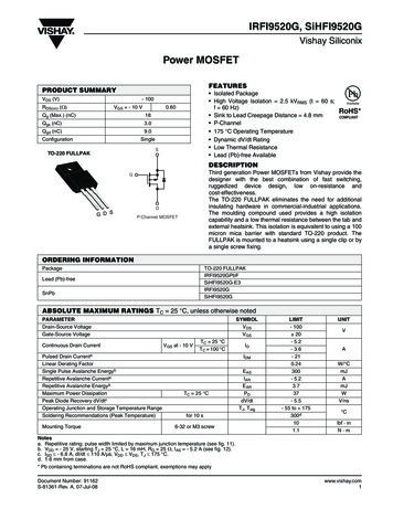
Transcription
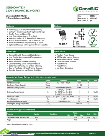
G2R1000MT33J3300 V 1000 mΩ SiC MOSFETTMSilicon Carbide MOSFETVDS RDS(ON)(Typ.) ID (TC 100 C) N-Channel Enhancement ModeFeatures PackageDSofter RDS(ON) v/s Temperature DependencyLoRing - Electromagnetically Optimized DesignSmaller RG(INT) and Lower QGLow Device Capacitances (COSS, CRSS)Industry-Leading UIL & Short-Circuit RobustnessRobust Body Diode with Low VF and Low QRRNormally Off-Stable Temperature up to 175 COptimized Package with Separate Driver Source PinGRoHSKSSD DrainG GateS SourceKS Kelvin SourceTO-263-7Advantages 3300 V1000 mΩ3AREACHApplicationsCompatible with Commercial Gate DriversLow Conduction Losses at all TemperaturesReduced RingingFaster and More Efficient SwitchingLesser Switching Spikes and Lower LossesBetter Power Density and System EfficiencyEase of Paralleling without Thermal RunawaySuperior Robustness and System Reliability Auxiliary Power Supply1500V Solar Inverter SystemsIndustrial Motors (AC Servos)General Purpose InvertersPulsed PowerPiezo DriversIon Beam GeneratorsAbsolute Maximum Ratings (At TC 25 C Unless Otherwise Stated)ParameterDrain-Source VoltageGate-Source Voltage (Dynamic)Gate-Source Voltage (Static)SymbolVDS(max)VGS(max)VGS(op)Continuous Forward CurrentIDPulsed Drain CurrentPower DissipationNon-Repetitive Avalanche EnergyOperating and Storage TemperatureID(pulse)PDEASTj , TstgConditionsVGS 0 V, ID 100 µARecommended OperationTC 25 C, VGS -5 / 20 VTC 100 C, VGS -5 / 20 VTC 135 C, VGS -5 / 20 VtP 3µs, D 1%, VGS 20 V, Note 1Tc 25 CL 150 mH, IAS 1.0 AValues3300-10 / 25-5 / 20532107475-55 to 175UnitVVVNoteAFig. 15AWmJ CFig. 14Fig. 16UnitNote C/WgFig. 13Thermal/Package CharacteristicsParameterSymbolThermal Resistance, Junction - ax.2.01Note 1: Pulse Width tP Limited by Tj(max)Rev 21/JunDownloaded from Arrow.com.Latest Version at: 0MT33J.pdfPage 1 of 14
G2R1000MT33J3300 V 1000 mΩ SiC MOSFETTMElectrical Characteristics (At TC 25 C Unless Otherwise Stated)ParameterSymbolConditionsDrain-Source Breakdown VoltageZero Gate Voltage Drain CurrentVDSSIDSSGate Source Leakage CurrentIGSSVGS 0 V, ID 100 µAVDS 3300 V, VGS 0 VVDS 0 V, VGS 25 VVDS 0 V, VGS -10 VVDS VGS, ID 2.0 mAVDS VGS, ID 2.0 mA, Tj 175 CVDS 10 V, ID 2 AVDS 10 V, ID 2 A, Tj 175 CVGS 20 V, ID 2 AVGS 20 V, ID 2 A, Tj 175 CGate Threshold VoltageVGS(th)TransconductancegfsDrain-Source On-State ResistanceInput CapacitanceOutput CapacitanceReverse Transfer CapacitanceCoss Stored EnergyCoss Stored ChargeEffective Output Capacitance (EnergyRelated)Effective Output Capacitance (TimeRelated)Gate-Source ChargeGate-Drain ChargeTotal Gate ChargeInternal Gate ResistanceTurn-On Switching Energy(Body Diode)Turn-Off Switching Energy(Body Diode)Turn-On Delay TimeRise TimeTurn-Off Delay TimeFall TimeRDS(ON)CissCossCrssEossQossVDS 1000 V, VGS 0 Vf 1 MHz, VAC fVDS 1000 V, VGS -5 / 20 VID 2 APer IEC607478-4f 1 MHz, VAC 25 mVTj 25 C, VGS -5/ 20V, RG(ext) 20 Ω, L 1800.0 µH, ID 2 A, VDD 1700 VVDD 1700 V, VGS -5/ 20VRG(ext) 20 Ω, L 1800.0 µH, ID 2 ATiming relative to VDS, Inductive 300nAVFig. 9SFig. 4mΩFig. 5-8pFFig. 11µJnCFig. 12pFNote 2nCFig. 10Ω51µJFig. 22,26nsFig. 241814241411*The chip technology was characterized up to 200 V/ns. The measured dV/dt was limited by measurement test setup and package.Note 2: Co(er), a lumped capacitance that gives same stored energy as C OSS while V DS is rising from 0 to 1000V.Co(tr), a lumped capacitance that gives same charging times as COSS while V DS is rising from 0 to 1000V.Rev 21/JunDownloaded from Arrow.com.Latest Version at: 0MT33J.pdfPage 2 of 14
G2R1000MT33J3300 V 1000 mΩ SiC MOSFETTMReverse Diode CharacteristicsParameterSymbolDiode Forward VoltageVSDContinuous Diode Forward CurrentDiode Pulse CurrentReverse Recovery TimeReverse Recovery ChargePeak Reverse Recovery CurrentReverse Recovery TimeReverse Recovery ChargePeak Reverse Recovery CurrentRev 21/JunDownloaded from sVGS -5 V, ISD 1 AVGS -5 V, ISD 1 A, Tj 175 CVGS -5 V, Tc 100 CVGS -5 V, Note 1VGS -5 V, ISD 2 A, VR 1700 Vdif/dt 1100 A/µs, Tj 25 CVGS -5 V, ISD 2 A, VR 1700 Vdif/dt 1100 A/µs, Tj 175 CMin.ValuesTyp.8.58.22819402241524Latest Version at: 0MT33J.pdfMax.UnitNoteVFig. 17-18AAnsnCAnsnCAPage 3 of 14
G2R1000MT33J3300 V 1000 mΩ SiC MOSFETFigure 1: Output Characteristics (Tj 25 C)ID f(VDS, VGS); tP 250 µsFigure 3: Output Characteristics (VGS 20 V)ID f(VDS, T);j tP 250 µsRev 21/JunDownloaded from Arrow.com.TMFigure 2: Output Characteristics (Tj 175 C)ID f(VDS, VGS); tP 250 µsFigure 4: Transfer Characteristics (VDS 10 V)ID f(VGS, T);j tP 100 µsLatest Version at: 0MT33J.pdfPage 4 of 14
G2R1000MT33J3300 V 1000 mΩ SiC MOSFETFigure 5: On-State Resistance v/s TemperatureRDS(ON) f(T,j VGS); tP 250 µs; ID 2 AFigure 7: Normalized On-State Resistance v/s TemperatureRDS(ON) f(T);j tP 250 µs; ID 2 A; VGS 20 VRev 21/JunDownloaded from Arrow.com.TMFigure 6: On-State Resistance v/s Drain CurrentRDS(ON) f(T,Ij D); tP 250 µs; VGS 20 VFigure 8: On-State Resistance v/s Gate VoltageRDS(ON) f(T,Vj GS); tP 250 µs; I D 2 ALatest Version at: 0MT33J.pdfPage 5 of 14
G2R1000MT33J3300 V 1000 mΩ SiC MOSFETFigure 9: Threshold Voltage CharacteristicsVGS(th) f(T);j VDS VGS; ID 2.0 mAFigure 11: Capacitance v/s Drain-Source Voltagef 1 MHz; VAC 25mVRev 21/JunDownloaded from Arrow.com.TMFigure 10: Gate Charge CharacteristicsID 2 A; VDS 1000 V; Tc 25 CFigure 12: Output Capacitor Stored EnergyEoss f(VDS)Latest Version at: 0MT33J.pdfPage 6 of 14
G2R1000MT33J3300 V 1000 mΩ SiC MOSFETFigure 13: Transient Thermal ImpedanceZth,jc f(tP,D); D tP/TFigure 15: Current De-rating CurveID f(TC); Tj 175 CRev 21/JunDownloaded from Arrow.com.TMFigure 14: Safe Operating Area (Tc 25 C)ID f(VDS, tP); Tj 175 C; D 0Figure 16: Power De-rating CurvePD f(TC); Tj 175 CLatest Version at: 0MT33J.pdfPage 7 of 14
G2R1000MT33J3300 V 1000 mΩ SiC MOSFETFigure 17: Body Diode Characteristics (Tj 25 C)ID f(VDS, VGS); tP 250 µsFigure 19: Third Quadrant Characteristics (Tj 25 C)ID f(VDS, VGS); tP 250 µsRev 21/JunDownloaded from Arrow.com.TMFigure 18: Body Diode Characteristics (Tj 175 C)ID f(VDS, VGS); tP 250 µsFigure 20: Third Quadrant Characteristics (Tj 175 C)ID f(VDS, VGS); tP 250 µsLatest Version at: 0MT33J.pdfPage 8 of 14
G2R1000MT33J3300 V 1000 mΩ SiC MOSFETFigure 21: Inductive Switching Energy v/s Drain Current(VDD 1500V)Tj 25 C; VGS -5/ 20V; RG(ext) 20 Ω; L 1800.0µHFigure 23: Inductive Switching Energy v/s RG(ext)(VDD 1700V)Tj 25 C; VGS -5/ 20V; IDS 2 A; L 1800.0µHRev 21/JunDownloaded from Arrow.com.TMFigure 22: Inductive Switching Energy v/s Drain Current(VDD 1700V)Tj 25 C; VGS -5/ 20V; RG(ext) 20 Ω; L 1800.0µHFigure 24: Switching Time v/s RG(ext)(VDD 1700V)Tj 25 C; VGS -5/ 20V; IDS 2 A; L 1800.0µHLatest Version at: 0MT33J.pdfPage 9 of 14
G2R1000MT33J3300 V 1000 mΩ SiC MOSFETFigure 25: Inductive Switching Energy v/s Temperature(VDD 1700V)Tj 25 C; VGS -5/ 20V; RG(ext) 20 Ω; IDS 2 A; L 1800.0µHRev 21/JunDownloaded from Arrow.com.TMFigure 26: dV/dt v/s RG(ext)(VDD 1700V)Tj 25 C; VGS -5/ 20V; IDS 2 A; L 1800.0µHLatest Version at: 0MT33J.pdfPage 10 of 14
G2R1000MT33J3300 V 1000 mΩ SiC MOSFETTMGate Charge CircuitGate Charge WaveformVGSD.U.TRLoadVDDIDIG(cont)Gate Voltage (VGS)VDSQGDQGSGate Charge (QG)Switching Time CircuitSwitching Time Waveform90%Same device as the D.U.T.LLoad-5 )trtonRev 21/JunDownloaded from Arrow.com.90%Latest Version at: 0MT33J.pdftftoffPage 11 of 14
G2R1000MT33J3300 V 1000 mΩ SiC MOSFETTMSwitching Energy CircuitSwitching Energy WaveformEOFF ID x VDS x dtEON ID x VDS x dtSame device as the D.U.T.LLoad-5 VIrrVDSVDSVGSVDDD.U.T.RGIDIDSReverse Recovery CircuitReverse Recovery WaveformD.U.T.LLoad-5 VIFtrrIF0 LevelVGSRGSame deviceas the D.U.T.90%VDDIrrdIrr/dt in 10%to 90% range10%Rev 21/JunDownloaded from Arrow.com.Latest Version at: 0MT33J.pdfPage 12 of 14
G2R1000MT33J3300 V 1000 mΩ SiC MOSFETTMPackage DimensionsTO-263-7 Package OutlineRecommended Solder Pad LayoutPackage View0.413(10.48)0.130(3.3)Case (D)0.249(6.32)0.640(16.25)0.0315(0.8)G0.126(3.2)KS S0.05(1.27)NOTE1. CONTROLLED DIMENSION IS INCH. DIMENSION IN BRACKET IS MILLIMETER.2. DIMENSIONS DO NOT INCLUDE END FLASH, MOLD FLASH, MATERIAL PROTRUSIONS.3. THE SOURCE AND KELVIN-SOURCE PINS ARE NOT INTERCHANGABLE. THEIR EXCHANGE MIGHT LEAD TO MALFUNCTION.Rev 21/JunDownloaded from Arrow.com.Latest Version at: 0MT33J.pdfPage 13 of 14
G2R1000MT33J3300 V 1000 mΩ SiC MOSFETTMComplianceRoHS ComplianceThe levels of RoHS restricted materials in this product are below the maximum concentration values (also referred to as the thresholdlimits) permitted for such substances, or are used in an exempted application, in accordance with EU Directive 2011/65/EC (RoHS 2), asadopted by EU member states on January 2, 2013 and amended on March 31, 2015 by EU Directive 2015/863. RoHS Declarations for thisproduct can be obtained from your GeneSiC representative.REACH ComplianceREACH substances of high concern (SVHCs) information is available for this product. Since the European Chemical Agency (ECHA) haspublished notice of their intent to frequently revise the SVHC listing for the foreseeable future, please contact a GeneSiC representative toinsure you get the most up-to-date REACH SVHC Declaration. REACH banned substance information (REACH Article 67) is also availableupon request.DisclaimerGeneSiC Semiconductor, Inc. reserves right to make changes to the product specifications and data in this document without notice.GeneSiC disclaims all and any warranty and liability arising out of use or application of any product. No license, express or implied to anyintellectual property rights is granted by this document.Unless otherwise expressly indicated, GeneSiC products are not designed, tested or authorized for use in life-saving, medical, aircraftnavigation, communication, air traffic control and weapons systems, nor in applications where their failure may result in death, personalinjury and/or property damage.Related Links SPICE 000MT33J/G2R1000MT33J SPICE.zip PLECS 000MT33J/G2R1000MT33J PLECS.zip CAD 000MT33J/G2R1000MT33J 3D.zip Gate Driver Reference: https://www.genesicsemi.com/technical-support Evaluation rt y Compliance:https://www.genesicsemi.com/compliance Quality Manual:https://www.genesicsemi.com/qualityRevision History Rev 21/Jun: Updated switching time and switching energy data Supersedes: Rev 20/Nov, Rev 21/Janwww.genesicsemi.com/sic-mosfet/Rev 21/JunCopyright 2021 GeneSiC Semiconductor Inc.All Rights Reserved.Downloaded from Arrow.com.Published by GeneSiC Semiconductor, Inc.43670 Trade Center Place Suite 155, Dulles, VA 20166; USAPage 14 of 14
3300 V 1000 m SiC MOSFET TM Reverse Diode Characteristics Parameter Symbol Conditions Values Unit Note Min. Typ. Max. Diode Forward Voltage V V -5 V, I 1 A 8.5 V Fig. 17-18 V -5 V, I 1 A, T 175 C 8.2 Continuous Diode Forward Current I V -5 V, T 100 C 2 A Diode Pulse Current I V -5 V, Note 1 8 A