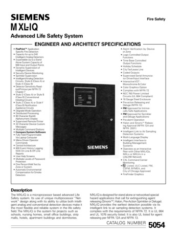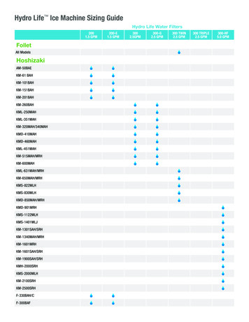
Transcription
Chipsmall Limited consists of a professional team with an average of over 10 year of expertise in the distributionof electronic components. Based in Hongkong, we have already established firm and mutual-benefit businessrelationships with customers from,Europe,America and south Asia,supplying obsolete and hard-to-find componentsto meet their specific needs.With the principle of “Quality Parts,Customers Priority,Honest Operation,and Considerate Service”,our businessmainly focus on the distribution of electronic components. Line cards we deal with ht and Freescale. Main products compriseIC,Modules,Potentiometer,IC Socket,Relay,Connector.Our parts cover such applications as commercial,industrial,and automotives areas.We are looking forward to setting up business relationship with you and hope to provide you with the best serviceand solution. Let us make a better world for our industry!Contact usTel: 86-755-8981 8866 Fax: 86-755-8427 6832Email & Skype: info@chipsmall.com Web: www.chipsmall.comAddress: A1208, Overseas Decoration Building, #122 Zhenhua RD., Futian, Shenzhen, China
Important noticeDear Customer,On 7 February 2017 the former NXP Standard Product business became a new company with thetradename Nexperia. Nexperia is an industry leading supplier of Discrete, Logic and PowerMOSsemiconductors with its focus on the automotive, industrial, computing, consumer and wearableapplication marketsIn data sheets and application notes which still contain NXP or Philips Semiconductors references, usethe references to Nexperia, as shown below.Instead of http://www.nxp.com, http://www.philips.com/ or http://www.semiconductors.philips.com/,use http://www.nexperia.comInstead of sales.addresses@www.nxp.com or sales.addresses@www.semiconductors.philips.com, usesalesaddresses@nexperia.com (email)Replace the copyright notice at the bottom of each page or elsewhere in the document, depending onthe version, as shown below:- NXP N.V. (year). All rights reserved or Koninklijke Philips Electronics N.V. (year). All rightsreservedShould be replaced with:- Nexperia B.V. (year). All rights reserved.If you have any questions related to the data sheet, please contact our nearest sales office via e-mailor telephone (details via salesaddresses@nexperia.com). Thank you for your cooperation andunderstanding,Kind regards,Team Nexperia
2N7002BKS60 V, 300 mA dual N-channel Trench MOSFETRev. 2 — 23 September 2010Product data sheet1. Product profile1.1 General descriptionDual N-channel enhancement mode Field-Effect Transistor (FET) in a very smallSOT363 (SC-88) Surface-Mounted Device (SMD) plastic package using Trench MOSFETtechnology.1.2 Features and benefits Logic-level compatibleVery fast switchingTrench MOSFET technologyESD protection up to 2 kVAEC-Q101 qualified1.3 Applications Relay driverHigh-speed line driverLow-side loadswitchSwitching circuits1.4 Quick reference dataTable 1.Quick reference -source voltageTamb 25 C--60VVGSgate-source voltageTamb 25 CIDdrain currentTamb 25 C;VGS 10 VRDSondrain-source on-stateresistanceTj 25 C;VGS 10 V;ID 500 mA[1][1]-- 20V--300mA-11.6ΩDevice mounted on an FR4 PCB, single-sided copper, tin-plated, mounting pad for drain 1 cm2.
2N7002BKSNXP Semiconductors60 V, 300 mA dual N-channel Trench MOSFET2. Pinning informationTable 2.PinningPinSymbolDescription1S1source 12G1gate 13D2drain 24S2source 25G2gate 26D1drain 1Simplified outline615Graphic symbol423162534017aaa0553. Ordering informationTable 3.Ordering informationType lastic surface-mounted package; 6 leadsSOT3634. MarkingTable 4.Marking codesType numberMarking code[1]2N7002BKSZT*[1]* -: made in Hong Kong* p: made in Hong Kong* t: made in Malaysia* W: made in China5. Limiting valuesTable 5.Limiting valuesIn accordance with the Absolute Maximum Rating System (IEC 60134).SymbolParameterConditionsMinMaxUnit-60V- 20VTamb 25 C-300mATamb 100 C-215mAPer transistorVDSdrain-source voltageTamb 25 CVGSgate-source voltageTamb 25 CID2N7002BKSProduct data sheetdrain currentVGS 10 VAll information provided in this document is subject to legal disclaimers.Rev. 2 — 23 September 2010[1] NXP B.V. 2010. All rights reserved.2 of 16
2N7002BKSNXP Semiconductors60 V, 300 mA dual N-channel Trench MOSFETTable 5.Limiting values continuedIn accordance with the Absolute Maximum Rating System (IEC 60134).SymbolParameterConditionsMinMaxUnitIDMpeak drain currentTamb 25 C;single pulse; tp 10 μs-1.2APtottotal power dissipationTamb 25 C[2]-295mW[1]-340mW-1040mWTsp 25 CSource-drain diodeTamb 25 C[1]-300mAelectrostatic dischargevoltagehuman body model[3]-2000VPtottotal power dissipationTamb 25 C[2]-445mWTjjunction temperature150 CTambambient temperature 55 150 CTstgstorage temperature 65 150 Csource currentISESD maximum ratingVESDPer device[1]Device mounted on an FR4 PCB, single-sided copper, tin-plated, mounting pad for drain 1 cm2.[2]Device mounted on an FR4 Printed-Circuit Board (PCB), single-sided copper, tin-plated and standardfootprint.[3]Measured between all pins.017aaa001120Pder(%)Ider(%)808040400 75 2525750 75125175Tamb ( C)P totP der ------------------------ 100 %P tot ( 25 C )Fig 1.017aaa002120Product data sheet2575125175Tamb ( C)IDI der -------------------- 100 %I D ( 25 C )Normalized total power dissipation as afunction of ambient temperature2N7002BKS 25Fig 2.Normalized continuous drain current as afunction of ambient temperatureAll information provided in this document is subject to legal disclaimers.Rev. 2 — 23 September 2010 NXP B.V. 2010. All rights reserved.3 of 16
2N7002BKSNXP Semiconductors60 V, 300 mA dual N-channel Trench MOSFET017aaa05610ID(A)Limit RDSon VDS/ID1(1)(2)10 1(3)(4)(5)10 2(6)10 310 1110210VDS (V)IDM single pulse(1) tp 100 μs(2) tp 1 ms(3) tp 10 ms(4) DC; Tsp 25 C(5) tp 100 ms(6) DC; Tamb 25 C; drain mounting pad 1 cm2Fig 3.Safe operating area; junction to ambient; continuous and peak drain currents as a function ofdrain-source voltage6. Thermal characteristicsTable 6.SymbolThermal -370425K/W[2]-320370K/W--120K/W--275K/WPer transistorRth(j-a)Rth(j-sp)thermal resistance fromjunction to ambientin free airthermal resistance fromjunction to solder pointPer deviceRth(j-a)2N7002BKSProduct data sheetthermal resistance fromjunction to ambientin free air[1][1]Device mounted on an FR4 PCB, single-sided copper, tin-plated and standard footprint.[2]Device mounted on an FR4 PCB, single-sided copper, tin-plated, mounting pad for drain 1 cm2.All information provided in this document is subject to legal disclaimers.Rev. 2 — 23 September 2010 NXP B.V. 2010. All rights reserved.4 of 16
2N7002BKSNXP Semiconductors60 V, 300 mA dual N-channel Trench MOSFET017aaa057103duty cycle .01110 310 210 1110102103tp (s)FR4 PCB, standard footprintFig 4.Transient thermal impedance from junction to ambient as a function of pulse duration; typical values017aaa058103duty cycle .01110 310 210 1110102103tp (s)FR4 PCB, mounting pad for drain 1 cm2Fig 5.Transient thermal impedance from junction to ambient as a function of pulse duration; typical values2N7002BKSProduct data sheetAll information provided in this document is subject to legal disclaimers.Rev. 2 — 23 September 2010 NXP B.V. 2010. All rights reserved.5 of 16
2N7002BKSNXP Semiconductors60 V, 300 mA dual N-channel Trench MOSFET7. CharacteristicsTable 7.CharacteristicsTj 25 C unless otherwise --V1.11.62.1VTj 25 C--1μATj 150 .470.751.1VStatic characteristicsV(BR)DSSdrain-source breakdown ID 10 μA; VGS 0 VvoltageVGS(th)gate-source thresholdvoltageID 250 μA; VDS VGSIDSSdrain leakage currentVDS 60 V; VGS 0 VIGSSRDSongate leakage currentdrain-source on-stateresistanceVGS 20 V; VDS 0 V[1]VGS 5 V; ID 50 mAVGS 10 V; ID 500 mAforwardtransconductancegfsVDS 10 V; ID 200 mA[1]Dynamic characteristicsQG(tot)total gate chargeQGSgate-source chargeQGDgate-drain chargeCissinput capacitanceCossoutput capacitanceCrssreverse transfercapacitancetd(on)turn-on delay timetrrise timetd(off)turn-off delay timetffall timeID 300 mA;VDS 30 V;VGS 4.5 VVGS 0 V; VDS 10 V;f 1 MHzVDD 50 V;RL 250 Ω;VGS 10 V;RG 6 ΩSource-drain diodeVSD[1]2N7002BKSProduct data sheetsource-drain voltageIS 115 mA; VGS 0 VPulse test: tp 300 μs; δ 0.01.All information provided in this document is subject to legal disclaimers.Rev. 2 — 23 September 2010 NXP B.V. 2010. All rights reserved.6 of 16
2N7002BKSNXP Semiconductors60 V, 300 mA dual N-channel Trench MOSFET017aaa0390.7VGS 4.0 VID(A)0.6017aaa04010 33.5 VID(A)3.25 V0.510 4(1)0.4(2)(3)3.0 V0.310 52.75 V0.22.5 V0.10.00.01.02.03.04.010 60.01.02.0VDS (V)3.0VGS (V)Tamb 25 CTamb 25 C; VDS 5 V(1) minimum values(2) typical values(3) maximum valuesFig 6.Output characteristics: drain current as afunction of drain-source voltage; typicalvaluesFig 7.017aaa0416.0RDSon(Ω)Sub-threshold drain current as a function ofgate-source .0(4)(2)(5)0.00.00.20.40.60.80.00.01.02.0ID (A)Tamb 25 C4.06.08.010.0VGS (V)ID 500 mA(1) VGS 3.25 V(1) Tamb 150 C(2) VGS 3.5 V(2) Tamb 25 C(3) VGS 4 V(4) VGS 5 V(5) VGS 10 VFig 8.Drain-source on-state resistance as a functionof drain current; typical values2N7002BKSProduct data sheetFig 9.Drain-source on-state resistance as a functionof gate-source voltage; typical valuesAll information provided in this document is subject to legal disclaimers.Rev. 2 — 23 September 2010 NXP B.V. 2010. All rights reserved.7 of 16
2N7002BKSNXP Semiconductors60 V, 300 mA dual N-channel Trench 61.20.40.60.20.00.01.02.03.04.05.0VGS (V)0.0 60VDS ID RDSon060120180Tamb ( C)R DSona ----------------------------R DSon ( 25 C )(1) Tamb 25 C(2) Tamb 150 CFig 10. Transfer characteristics: drain current as afunction of gate-source voltage; typical values017aaa0453.0VGS(th)(V)Fig 11. Normalized drain-source on-state resistanceas a function of ambient temperature; (3)1.00.0 60060120180Tamb ( C)110 1f 1 MHz; VGS 0 VID 0.25 mA; VDS VGS(1) Ciss(2) typical values(2) Coss(3) minimum values(3) CrssFig 12. Gate-source threshold voltage as a function ofambient temperatureProduct data sheet10210VDS (V)(1) maximum values2N7002BKS1Fig 13. Input, output and reverse transfercapacitances as a function of drain-sourcevoltage; typical valuesAll information provided in this document is subject to legal disclaimers.Rev. 2 — 23 September 2010 NXP B.V. 2010. All rights reserved.8 of 16
2N7002BKSNXP Semiconductors60 V, 300 mA dual N-channel Trench h)VGS1.0QGS10.00.0QGS2QGS0.20.40.60.8QG (nC)QGDQG(tot)003aaa508ID 300 mA; VDD 6 V; Tamb 25 CFig 14. Gate-source voltage as a function of gatecharge; typical valuesFig 15. Gate charge waveform .81.2VSD (V)VGS 0 V(1) Tamb 150 C(2) Tamb 25 CFig 16. Source current as a function of source-drain voltage; typical values2N7002BKSProduct data sheetAll information provided in this document is subject to legal disclaimers.Rev. 2 — 23 September 2010 NXP B.V. 2010. All rights reserved.9 of 16
2N7002BKSNXP Semiconductors60 V, 300 mA dual N-channel Trench MOSFET8. Test informationPduty cycle δ t2t1t2t1t006aaa812Fig 17. Duty cycle definition2N7002BKSProduct data sheetAll information provided in this document is subject to legal disclaimers.Rev. 2 — 23 September 2010 NXP B.V. 2010. All rights reserved.10 of 16
2N7002BKSNXP Semiconductors60 V, 300 mA dual N-channel Trench MOSFET9. Package outlinePlastic surface-mounted package; 6 leadsSOT363DEByXAHE65v M A4Qpin 1indexAA112e13bpcLpw M Bedetail X012 mmscaleDIMENSIONS (mm are the original T363JEITASC-88EUROPEANPROJECTIONISSUE DATE04-11-0806-03-16Fig 18. Package outline SOT363 (SC-88)2N7002BKSProduct data sheetAll information provided in this document is subject to legal disclaimers.Rev. 2 — 23 September 2010 NXP B.V. 2010. All rights reserved.11 of 16
2N7002BKSNXP Semiconductors60 V, 300 mA dual N-channel Trench MOSFET10. Soldering2.65solder lands2.35 1.50.4 (2 )0.6 0.5(4 ) (4 )solder resistsolder paste0.5(4 )0.6(2 )occupied area0.6(4 )Dimensions in mm1.8sot363 frFig 19. Reflow soldering footprint SOT363 (SC-88)1.5solder lands0.3 2.54.5solder resistoccupied area1.5Dimensions in mm1.31.3preferred transportdirection during soldering2.455.3sot363 fwFig 20. Wave soldering footprint SOT363 (SC-88)2N7002BKSProduct data sheetAll information provided in this document is subject to legal disclaimers.Rev. 2 — 23 September 2010 NXP B.V. 2010. All rights reserved.12 of 16
2N7002BKSNXP Semiconductors60 V, 300 mA dual N-channel Trench MOSFET11. Revision historyTable 8.Revision historyDocument IDRelease dateData sheet statusChange noticeSupersedes2N7002BKS v.220100923Product data sheet-2N7002BKS v.1--Modifications:2N7002BKS v.12N7002BKSProduct data sheet Table 2 “Pinning”: graphic symbol amended20100617Product data sheetAll information provided in this document is subject to legal disclaimers.Rev. 2 — 23 September 2010 NXP B.V. 2010. All rights reserved.13 of 16
2N7002BKSNXP Semiconductors60 V, 300 mA dual N-channel Trench MOSFET12. Legal information12.1 Data sheet statusDocument status[1][2]Product status[3]DefinitionObjective [short] data sheetDevelopmentThis document contains data from the objective specification for product development.Preliminary [short] data sheetQualificationThis document contains data from the preliminary specification.Product [short] data sheetProductionThis document contains the product specification.[1]Please consult the most recently issued document before initiating or completing a design.[2]The term ‘short data sheet’ is explained in section “Definitions”.[3]The product status of device(s) described in this document may have changed since this document was published and may differ in case of multiple devices. The latest product statusinformation is available on the Internet at URL http://www.nxp.com.12.2 DefinitionsDraft — The document is a draft version only. The content is still underinternal review and subject to formal approval, which may result inmodifications or additions. NXP Semiconductors does not give anyrepresentations or warranties as to the accuracy or completeness ofinformation included herein and shall have no liability for the consequences ofuse of such information.Short data sheet — A short data sheet is an extract from a full data sheetwith the same product type number(s) and title. A short data sheet is intendedfor quick reference only and should not be relied upon to contain detailed andfull information. For detailed and full information see the relevant full datasheet, which is available on request via the local NXP Semiconductors salesoffice. In case of any inconsistency or conflict with the short data sheet, thefull data sheet shall prevail.Product specification — The information and data provided in a Productdata sheet shall define the specification of the product as agreed betweenNXP Semiconductors and its customer, unless NXP Semiconductors andcustomer have explicitly agreed otherwise in writing. In no event however,shall an agreement be valid in which the NXP Semiconductors product isdeemed to offer functions and qualities beyond those described in theProduct data sheet.12.3 DisclaimersLimited warranty and liability — Information in this document is believed tobe accurate and reliable. However, NXP Semiconductors does not give anyrepresentations or warranties, expressed or implied, as to the accuracy orcompleteness of such information and shall have no liability for theconsequences of use of such information.In no event shall NXP Semiconductors be liable for any indirect, incidental,punitive, special or consequential damages (including - without limitation - lostprofits, lost savings, business interruption, costs related to the removal orreplacement of any products or rework charges) whether or not suchdamages are based on tort (including negligence), warranty, breach ofcontract or any other legal theory.Notwithstanding any damages that customer might incur for any reasonwhatsoever, NXP Semiconductors’ aggregate and cumulative liability towardscustomer for the products described herein shall be limited in accordancewith the Terms and conditions of commercial sale of NXP Semiconductors.malfunction of an NXP Semiconductors product can reasonably be expectedto result in personal injury, death or severe property or environmentaldamage. NXP Semiconductors accepts no liability for inclusion and/or use ofNXP Semiconductors products in such equipment or applications andtherefore such inclusion and/or use is at the customer’s own risk.Applications — Applications that are described herein for any of theseproducts are for illustrative purposes only. NXP Semiconductors makes norepresentation or warranty that such applications will be suitable for thespecified use without further testing or modification.Customers are responsible for the design and operation of their applicationsand products using NXP Semiconductors products, and NXP Semiconductorsaccepts no liability for any assistance with applications or customer productdesign. It is customer’s sole responsibility to determine whether the NXPSemiconductors product is suitable and fit for the customer’s applications andproducts planned, as well as for the planned application and use ofcustomer’s third party customer(s). Customers should provide appropriatedesign and operating safeguards to minimize the risks associated with theirapplications and products.NXP Semiconductors does not accept any liability related to any default,damage, costs or problem which is based on any weakness or default in thecustomer’s applications or products, or the application or use by customer’sthird party customer(s). Customer is responsible for doing all necessarytesting for the customer’s applications and products using NXPSemiconductors products in order to avoid a default of the applications andthe products or of the application or use by customer’s third partycustomer(s). NXP does not accept any liability in this respect.Limiting values — Stress above one or more limiting values (as defined inthe Absolute Maximum Ratings System of IEC 60134) will cause permanentdamage to the device. Limiting values are stress ratings only and (proper)operation of the device at these or any other conditions above those given inthe Recommended operating conditions section (if present) or theCharacteristics sections of this document is not warranted. Constant orrepeated exposure to limiting values will permanently and irreversibly affectthe quality and reliability of the device.Terms and conditions of commercial sale — NXP Semiconductorsproducts are sold subject to the general terms and conditions of commercialsale, as published at http://www.nxp.com/profile/terms, unless otherwiseagreed in a valid written individual agreement. In case an individualagreement is concluded only the terms and conditions of the respectiveagreement shall apply. NXP Semiconductors hereby expressly objects toapplying the customer’s general terms and conditions with regard to thepurchase of NXP Semiconductors products by customer.Right to make changes — NXP Semiconductors reserves the right to makechanges to information published in this document, including withoutlimitation specifications and product descriptions, at any time and withoutnotice. This document supersedes and replaces all information supplied priorto the publication hereof.No offer to sell or license — Nothing in this document may be interpreted orconstrued as an offer to sell products that is open for acceptance or the grant,conveyance or implication of any license under any copyrights, patents orother industrial or intellectual property rights.Suitability for use — NXP Semiconductors products are not designed,authorized or warranted to be suitable for use in life support, life-critical orsafety-critical systems or equipment, nor in applications where failure orExport control — This document as well as the item(s) described hereinmay be subject to export control regulations. Export might require a priorauthorization from national authorities.2N7002BKSProduct data sheetAll information provided in this document is subject to legal disclaimers.Rev. 2 — 23 September 2010 NXP B.V. 2010. All rights reserved.14 of 16
2N7002BKSNXP Semiconductors60 V, 300 mA dual N-channel Trench MOSFETQuick reference data — The Quick reference data is an extract of theproduct data given in the Limiting values and Characteristics sections of thisdocument, and as such is not complete, exhaustive or legally binding.12.4 TrademarksNotice: All referenced brands, product names, service names and trademarksare the property of their respective owners.13. Contact informationFor more information, please visit: http://www.nxp.comFor sales office addresses, please send an email to: salesaddresses@nxp.com2N7002BKSProduct data sheetAll information provided in this document is subject to legal disclaimers.Rev. 2 — 23 September 2010 NXP B.V. 2010. All rights reserved.15 of 16
2N7002BKSNXP Semiconductors60 V, 300 mA dual N-channel Trench MOSFET14. 41314Product profile . . . . . . . . . . . . . . . . . . . . . . . . . . 1General description . . . . . . . . . . . . . . . . . . . . . 1Features and benefits . . . . . . . . . . . . . . . . . . . . 1Applications . . . . . . . . . . . . . . . . . . . . . . . . . . . 1Quick reference data . . . . . . . . . . . . . . . . . . . . 1Pinning information . . . . . . . . . . . . . . . . . . . . . . 2Ordering information . . . . . . . . . . . . . . . . . . . . . 2Marking . . . . . . . . . . . . . . . . . . . . . . . . . . . . . . . . 2Limiting values. . . . . . . . . . . . . . . . . . . . . . . . . . 2Thermal characteristics . . . . . . . . . . . . . . . . . . 4Characteristics . . . . . . . . . . . . . . . . . . . . . . . . . . 6Test information . . . . . . . . . . . . . . . . . . . . . . . . 10Package outline . . . . . . . . . . . . . . . . . . . . . . . . 11Soldering . . . . . . . . . . . . . . . . . . . . . . . . . . . . . 12Revision history . . . . . . . . . . . . . . . . . . . . . . . . 13Legal information. . . . . . . . . . . . . . . . . . . . . . . 14Data sheet status . . . . . . . . . . . . . . . . . . . . . . 14Definitions . . . . . . . . . . . . . . . . . . . . . . . . . . . . 14Disclaimers . . . . . . . . . . . . . . . . . . . . . . . . . . . 14Trademarks. . . . . . . . . . . . . . . . . . . . . . . . . . . 15Contact information. . . . . . . . . . . . . . . . . . . . . 15Contents . . . . . . . . . . . . . . . . . . . . . . . . . . . . . . 16Please be aware that important notices concerning this document and the product(s)described herein, have been included in section ‘Legal information’. NXP B.V. 2010.All rights reserved.For more information, please visit: http://www.nxp.comFor sales office addresses, please send an email to: salesaddresses@nxp.comDate of release: 23 September 2010Document identifier: 2N7002BKS
60 V, 300 mA dual N-channel Trench MOSFET Rev. 2 — 23 September 2010 Product data sheet Symbol Parameter Conditions Min Typ Max Unit VDS drain-source voltage Tamb 25 C--60V VGS gate-source voltage Tamb 25 C-- 20 V ID drain current Tamb 25 C; VGS 10V [1]-- 300mA RDSon drain-source on-state resistance