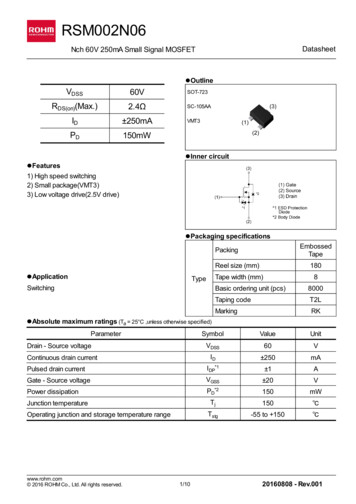
Transcription
Class 02: Transistors ITopics: What is a transistor? History of transistors Views of an n-type transistor schematic and cross section channel length, channel width Where are we headed? Final cross section for CMOS CMOS vs. NMOS Layout layers for a transistor Layout and Cross section for an NMOS transistor CMOS Formation Substrate and Doping Why Isolate? Isolation, Nwell Vt Adjust Poly P Diffusion N Diffusion Final Cross Section for CMOS1/16/01Joseph A. Elias, PhD1
Class 02: Transistors ITransistor - trans(fer) (res)istor NFET (PFET) - n-type (p-type) field effect transistor NMOS (PMOS) - n-type (p-type) metal oxide semiconductor (misnomer) MESFET - metal semiconductor FET MISFET - metal insulator FET IGFET - insulated gate FET JFET - junction FET (BJT - Bipolar Junction Transistor) History: 1875 - Selenium shown to have rectifying and optoelectronic properties 1906 - Silicon used for diode to detect radio waves 1935 - Selenium rectifiers and photodetectors commercially availabe WWII - Radar spurs growth of Silicon and Germanium research 1948 - Point contact transistor by Bardeen and Brattain (Bell Labs) 1949 - Junction diodes and junction transistors by Shockley (Bell Labs) 1949 - Single crystal (as opposed to polycrystalline) silicon developed 1952 - Grown junction germanium transistors by Shockley (Bell Labs) 1954 - Grown junction silicon transistors by Texas Instruments 1959 - Integrated circuit by Kilby (Texas Instruments) 1961 - Silicon planar transistor by Hoerni (Fairchild)(References: Runyan and Bean, Yang, Sze)1/16/01Joseph A. Elias, PhD2
Class 02: Transistors INMOS Cross Section (Martin p.91)A transistorhas four terminalssourcegatedrainSubstrate, bulk, well, or back gateWhy is this important? W, L, S, D, G are fundamental to every aspect of IC design(circuit level, gate level, layout, simulation) Each transistor is the basically the same, so know one, you know them all1/16/01Joseph A. Elias, PhD3
Class 02: Transistors IFinal Cross Section for CMOS (Martin p. 47)CrossSectionPartialLayoutWhy is this important? Design Engineers: understanding of how transistors are formed leads to better designs Process Engineers: each step in the formation is related to the next Product Engineers: debugging of product-level issues involves cross section CAD/Layout Engineers: integrating rules and determining violations to layout1/16/01Joseph A. Elias, PhD4
Class 02: Transistors ICMOS vs. NMOSCMOS - Complementary Metal Oxide SemiconductorNMOS - N-type Metal Oxide SemiconductorAssumptions for CMOS: Substrate is p-type Gate material is made of polysilicon The process is single-well (nwell)CMOS vs. NMOS: NMOS process uses n-type transistors only CMOS (complementary MOS) uses n- and p-type NMOS process has a substrate (p-type) no wells CMOS process has a substrate (p-type) and(usually) one well (nwell)1/16/01Joseph A. Elias, PhD5
Class 02: Transistors ILayout Layers for TransistorDrawn and MASK layers used to create a transistor:1) Well (aka substrate, tub, moat) nmos are in pwell, pmos are in nwell2) Diffusion , ACTIVE, NSELECT, PSELECT (aka diff) type of diffusion for Source/Drain set by well defines active vs. isolation (or field) regions3) Poly (aka gate) gate material over diff defines W and L of transistor4) Contact , CT-TO-ACTIVE, CT-TO-POLY (aka ct) defines how the source, drain, gate, and tap are contacted to higher levels5) Tap, ACTIVE, NSELECT, PSELECT defines contact to substrate or well heavily doped, same type as sub/well (i.e., n-type in nwell, p-type in p-substrate)1/16/01Joseph A. Elias, PhD6
Class 02: Transistors ILayout and Cross Section - NMOS (Martin IsolationRegion1/16/01Joseph A. Elias, PhD7
Class 02: Transistors ICMOS Formation - Substrate, DopingResearch Areas:II-VIIII-V Presently, most starting material (substrate) is 100 p-type silicon Silicon is a group IV element (4 outer electrons) p-type dopants are ones with less electrons, or more holes (B) n-type dopants are ones with more electrons, or less holes (P, As)1/16/01Joseph A. Elias, PhD8
Class 02: Transistors ICMOS Formation - Why isolate? (Wolf p.18)1/16/01Joseph A. Elias, PhD9
Class 02: Transistors ICMOS Formation - Isolation, Nwell (Martin p.42)nwellDiff-tap Deposit SiO2, Si3N4, photoresist (PR) Use DiffTap (aka moat, active) mask to define isolation regions. This is wheretransistors will NOT be located, which is the inverse of diffusion and tap regions Grow isolation (LOCOS), or etch silicon and deposit oxide (STI), strip Si3N4 Deposit photoresist, expose NWELL mask, develop, implant N-type well (Phos) Optional : Implant field regions for channel stop (CS), punchthrough (PT)1/16/01Joseph A. Elias, PhD1
Class 02: Transistors ICMOS Formation - Vt Adjust (Martin p.43)nwellDiff-tapImplant will show up hereas well, but be counter-dopedlater in the process The order of events can vary, but in general: With NWELL pattern still on silicon, implant gate threshold adjust Strip thin oxide, regrow oxide to 30-100A (depending on process node) Done since oxide has been damaged due to implant Allows for gate oxide to be as clean as possible Purpose of Vt adjust will become apparent further in the semester1/16/01Joseph A. Elias, PhD1
Class 02: Transistors ICMOS Formation - Poly (Martin p. 44)nwellDiff-tappoly Deposit polysilcon everywhere on wafer, deposit PR Use POLY mask to define regions where poly is to remain Expose, develop PR; etch polysilicon; implant poly with P or As1/16/01Joseph A. Elias, PhD1
Class 02: Transistors ICMOS Formation - P diffusion (Martin p.45)PdiffnwellDiff-tappoly Use Diff-Tap layout to generate, or manually draw p-diff mask Size up the diff-tap region to account for misalignment Implant is self-aligned to gate, as gate acts as a mask1/16/01Joseph A. Elias, PhD1
Class 02: Transistors ICMOS Formation - N diffusion (Martin p. 45)PdiffnwellNdiffpolyIncorrecttap to well Use Diff-Tap layout to generate, or manually draw n-diff mask Size up the diff-tap region to account for misalignment Implant is self-aligned to gate, as gate acts as a mask Taps should NOT cross well boundaries!1/16/01Joseph A. Elias, PhD1
Class 02: Transistors IFinal Cross Section for CMOS (Martin p. 47) Further processing: CT (contact) mask to open up regions in thin oxide to contact diff CT (contact) mask to open up regions over poly to contact gates Deposition of ILD (inter-level dielectric) , shown as CVD SiO2 MET1 (metal 1) mask to identify routing Deposition of ILD, VIA mask to contact MET1, MET2 mask to route Deposition of PO (protective oxide), shown as Overglass1/16/01Joseph A. Elias, PhD1
Drawn and MASK layers used to create a transistor: 1) W ell (aka substrate, tub, moat) nmos are in pwell, pmos are in nwell 2) Diffusion , ACTIVE, NSELECT, PSELECT (aka diff) type of diffusion for Source/Drain set by well defines active vs. isolation (or field) regions 3) Poly (aka gate) gate material over diff defines W and L of transistor