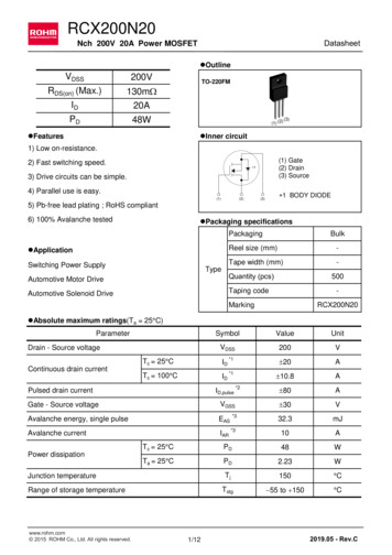
Transcription
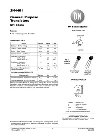
2N4401General PurposeTransistorsNPN Siliconhttp://onsemi.comFeatures Pb Free Packages are Available*COLLECTOR3MAXIMUM RATINGSRatingSymbolValueUnitCollector Emitter VoltageVCEO40VdcCollector Base VoltageVCBO60VdcEmitter Base VoltageVEBO6.0VdcCollector Current ContinuousIC600mAdcTotal Device Dissipation@ TA 25 CDerate above 25 CPD6255.0mWmW/ CTotal Device Dissipation@ TC 25 CDerate above 25 CPD1.512WmW/ CTJ, Tstg 55 to 150 COperating and Storage JunctionTemperature RangeTHERMAL CHARACTERISTICSCharacteristicSymbolMaxUnitThermal Resistance, Junction to AmbientRqJA200 C/WThermal Resistance, Junction to CaseRqJC83.3 C/WStresses exceeding Maximum Ratings may damage the device. MaximumRatings are stress ratings only. Functional operation above the RecommendedOperating Conditions is not implied. Extended exposure to stresses above theRecommended Operating Conditions may affect device reliability.2BASE1EMITTERTO 92CASE 29STYLE 11123STRAIGHT LEADBULK PACK23BENT LEADTAPE & REELAMMO PACKMARKING DIAGRAM2N4401AYWW GG2N4401 Device CodeA Assembly LocationY YearWW Work WeekG Pb Free Package(Note: Microdot may be in either location)ORDERING INFORMATIONSee detailed ordering and shipping information in the packagedimensions section on page 2 of this data sheet.*For additional information on our Pb Free strategy and soldering details, pleasedownload the ON Semiconductor Soldering and Mounting Techniques ReferenceManual, SOLDERRM/D. Semiconductor Components Industries, LLC, 2010February, 2010 Rev. 41Publication Order Number:2N4401/D
2N4401ELECTRICAL CHARACTERISTICS (TA 25 C unless otherwise noted)CharacteristicSymbolMinMaxUnitOFF CHARACTERISTICSCollector Emitter Breakdown Voltage (Note 1)(IC 1.0 mAdc, IB 0)V(BR)CEO40 VdcCollector Base Breakdown Voltage(IC 0.1 mAdc, IE 0)V(BR)CBO60 Vdc(IE 0.1 mAdc, IC 0)Emitter Base Breakdown VoltageV(BR)EBO6.0 VdcBase Cutoff Current(VCE 35 Vdc, VEB 0.4 Vdc)IBEV 0.1mAdcCollector Cutoff Current(VCE 35 Vdc, VEB 0.4 Vdc)ICEX 0.1mAdc20408010040 300 ON CHARACTERISTICS (Note 1)DC Current Gain(IC 0.1 mAdc, VCE 1.0 Vdc)(IC 1.0 mAdc, VCE 1.0 Vdc)(IC 10 mAdc, VCE 1.0 Vdc)(IC 150 mAdc, VCE 1.0 Vdc)(IC 500 mAdc, VCE 2.0 Vdc)hFE Collector Emitter Saturation Voltage(IC 150 mAdc, IB 15 mAdc)(IC 500 mAdc, IB 50 mAdc)VCE(sat) 0.40.75VdcBase Emitter Saturation Voltage(IC 150 mAdc, IB 15 mAdc)(IC 500 mAdc, IB 50 mAdc)VBE(sat)0.75 0.951.2VdcSMALL SIGNAL CHARACTERISTICSCurrent Gain Bandwidth Product(IC 20 mAdc, VCE 10 Vdc, f 100 MHz)fT250 MHzCollector Base Capacitance(VCB 5.0 Vdc, IE 0, f 1.0 MHz)Ccb 6.5pFEmitter Base Capacitance(VEB 0.5 Vdc, IC 0, f 1.0 MHz)Ceb 30pFInput Impedance(IC 1.0 mAdc, VCE 10 Vdc, f 1.0 kHz)hie1.015kWVoltage Feedback Ratio(IC 1.0 mAdc, VCE 10 Vdc, f 1.0 kHz)hre0.18.0X 10 4Small Signal Current Gain(IC 1.0 mAdc, VCE 10 Vdc, f 1.0 kHz)hfe40500 Output Admittance(IC 1.0 mAdc, VCE 10 Vdc, f 1.0 kHz)hoe1.030mmhos(VCC 30 Vdc, VBE 2.0 Vdc,IC 150 mAdc, IB1 15 mAdc)td 15nstr 20ns(VCC 30 Vdc, IC 150 mAdc,IB1 IB2 15 mAdc)ts 225nstf 30nsSWITCHING CHARACTERISTICSDelay TimeRise TimeStorage TimeFall Time1. Pulse Test: Pulse Width 300 ms, Duty Cycle 2.0%.ORDERING INFORMATIONPackageShipping†TO 925000 Units / BulkTO 92(Pb Free)5000 Units / BulkTO 922000 / Tape & Reel2N4401RLRAGTO 92(Pb Free)2000 / Tape & Reel2N4401RLRMGTO 92(Pb Free)2000 / Tape & Ammo BoxTO 922000 / Tape & Ammo BoxTO 92(Pb Free)2000 / Tape & Ammo RPG†For information on tape and reel specifications, including part orientation and tape sizes, please refer to our Tape and Reel PackagingSpecifications Brochure, BRD8011/D.http://onsemi.com2
2N4401SWITCHING TIME EQUIVALENT TEST CIRCUITS 30 V 30 V1.0 to 100 ms,DUTY CYCLE 2.0% 16 V0- 2.0 V200 W1.0 to 100 ms,DUTY CYCLE 2.0% 16 V200 W01.0 kW 2.0 ns1.0 kW-14 VCS* 10 pFCS* 10 pF 20 ns- 4.0 VScope rise time 4.0 ns*Total shunt capacitance of test jig connectors, and oscilloscopeFigure 1. Turn On TimeFigure 2. Turn Off TimeTRANSIENT CHARACTERISTICS25 C100 1VCC 30 VIC/IB 103.0CoboQ, CHARGE (nC)CAPACITANCE (pF)20QA0.10.2 0.3 0.51.02.0 3.0 5.010REVERSE VOLTAGE (VOLTS)20 305010203050 70 100200IC, COLLECTOR CURRENT (mA)Figure 3. Capacitances500Figure 4. Charge Data100100IC/IB 1070VCC 30 VIC/IB 1070tr5050tr @ VCC 30 Vtr @ VCC 10 Vtd @ VEB 2.0 Vtd @ VEB 03020t, TIME (ns)t, TIME 50020305070100200IC, COLLECTOR CURRENT (mA)IC, COLLECTOR CURRENT (mA)Figure 5. Turn On TimeFigure 6. Rise and Fall Timeshttp://onsemi.com3300500
2N4401300100ts′ ts - 1/8 tfIB1 IB2IC/IB 10 to 20VCC 30 VIB1 IB27050t f , FALL TIME (ns)t s′, STORAGE TIME (ns)20010070IC/IB 203020IC/IB 00IC, COLLECTOR CURRENT (mA)IC, COLLECTOR CURRENT (mA)Figure 7. Storage TimeFigure 8. Fall Time300500SMALL SIGNAL CHARACTERISTICSNOISE FIGUREVCE 10 Vdc, TA 25 C; Bandwidth 1.0 Hz10f 1.0 kHzRS OPTIMUMRS SOURCERS RESISTANCE8.0NF, NOISE FIGURE (dB)NF, NOISE FIGURE (dB)8.010IC 1.0 mA, RS 150 WIC 500 mA, RS 200 WIC 100 mA, RS 2.0 kWIC 50 mA, RS 4.0 kW6.04.02.0IC 50 mAIC 100 mAIC 500 mAIC 1.0 mA6.04.02.000.01 0.02 0.05 0.1 0.2 0.5 1.0 2.0 5.0f, FREQUENCY (kHz)010205010050Figure 9. Frequency Effects100 200500 1.0 k 2.0 k 5.0 k 10 k 20 kRS, SOURCE RESISTANCE (OHMS)50 k 100 kFigure 10. Source Resistance Effectshttp://onsemi.com4
2N4401h PARAMETERSVCE 10 Vdc, f 1.0 kHz, TA 25 CThis group of graphs illustrates the relationship betweenhfe and other “h” parameters for this series of transistors. Toobtain these curves, a high gain and a low gain unit wereselected from the 2N4401 lines, and the same units wereused to develop the correspondingly numbered curves oneach graph.50 khfe , CURRENT GAIN200100702N4401 UNIT 12N4401 UNIT 250300.10.20.30.5 0.7 1.02.03.020 k10 k5.0 k2.0 k1.0 k0.10.20.30.5 0.71.02.03.0IC, COLLECTOR CURRENT (mA)IC, COLLECTOR CURRENT (mA)Figure 11. Current GainFigure 12. Input Impedance105.0 7.0 101007.05.02N4401 UNIT 12N4401 UNIT 23.02.01.00.70.50.30.22N4401 UNIT 12N4401 UNIT 25005.0 7.0 10hoe , OUTPUT ADMITTANCE (m mhos)h re , VOLTAGE FEEDBACK RATIO (X 10-4 )20hie , INPUT IMPEDANCE (OHMS)3000.10.20.30.5 0.7 1.02.03.05020105.02N4401 UNIT 12N4401 UNIT 22.01.05.0 7.0 100.10.20.30.5 0.7 1.02.0 3.0IC, COLLECTOR CURRENT (mA)IC, COLLECTOR CURRENT (mA)Figure 13. Voltage Feedback RatioFigure 14. Output Admittancehttp://onsemi.com55.0 7.0 10
2N4401STATIC CHARACTERISTICSh FE , NORMALIZED CURRENT GAIN3.0VCE 1.0 VVCE 10 V2.0TJ 125 C1.025 C0.70.5- 55 C0.30.20.10.20.30.50.71.02.03.05.0 7.0 1020IC, COLLECTOR CURRENT (mA)305070100200300500VCE , COLLECTOR-EMITTER VOLTAGE (VOLTS)Figure 15. DC Current Gain1.0TJ 25 C0.80.6IC 1.0 mA10 mA100 mA500 mA0.40.200.010.02 0.030.05 0.07 0.10.20.30.5 0.7 1.0IB, BASE CURRENT (mA)2.03.05.0 7.010203050Figure 16. Collector Saturation Region1.0 0.5TJ 25 CVBE(sat) @ IC/IB 100.60COEFFICIENT (mV/ C)VOLTAGE (VOLTS)0.8VBE @ VCE 10 V0.40.2VCE(sat) @ IC/IB 100.5501.0 2.0 5.0 10 20IC, COLLECTOR CURRENT (mA)- 0.5- 1.0- 1.5- 2.000.1 0.2qVC for VCE(sat)100 200- 2.50.1 0.2500Figure 17. “On” VoltagesqVB for VBE0.5501.0 2.05.0 10 20IC, COLLECTOR CURRENT (mA)100 200Figure 18. Temperature Coefficientshttp://onsemi.com6500
MECHANICAL CASE OUTLINEPACKAGE DIMENSIONSTO 92 (TO 226)CASE 29 11ISSUE AMSCALE 1:11123STRAIGHT LEADBULK PACKDATE 09 MAR 200723BENT LEADTAPE & REELAMMO PACKABNOTES:1. DIMENSIONING AND TOLERANCING PER ANSIY14.5M, 1982.2. CONTROLLING DIMENSION: INCH.3. CONTOUR OF PACKAGE BEYOND DIMENSION RIS UNCONTROLLED.4. LEAD DIMENSION IS UNCONTROLLED IN P ANDBEYOND DIMENSION K MINIMUM.STRAIGHT LEADBULK PACKRPLSEATINGPLANEKDIMABCDGHJKLNPRVDX XGJHVCSECTION X OTES:1. DIMENSIONING AND TOLERANCING PERASME Y14.5M, 1994.2. CONTROLLING DIMENSION: MILLIMETERS.3. CONTOUR OF PACKAGE BEYONDDIMENSION R IS UNCONTROLLED.4. LEAD DIMENSION IS UNCONTROLLED IN PAND BEYOND DIMENSION K MINIMUM.BENT LEADTAPE & REELAMMO PACKBPTSEATINGPLANEGKDIMABCDGJKNPRVDX XJV1CNSECTION X --STYLES ON PAGE 2DOCUMENT NUMBER:STATUS:98ASB42022BON SEMICONDUCTOR STANDARDNEW STANDARD: Semiconductor Components Industries, LLC, 2002October, DESCRIPTION:2002 Rev. 0TO 92 (TO 226)http://onsemi.com1Electronic versions are uncontrolled except whenaccessed directly from the Document Repository. Printedversions are uncontrolled except when stamped“CONTROLLED COPY” in red.Case Outline Number:PAGE 1 OFXXX3
TO 92 (TO 226)CASE 29 11ISSUE AMDATE 09 MAR 2007STYLE 1:PIN 1. EMITTER2. BASE3. COLLECTORSTYLE 2:PIN 1. BASE2. EMITTER3. COLLECTORSTYLE 3:PIN 1. ANODE2. ANODE3. CATHODESTYLE 4:PIN 1. CATHODE2. CATHODE3. ANODESTYLE 5:PIN 1. DRAIN2. SOURCE3. GATESTYLE 6:PIN 1. GATE2. SOURCE & SUBSTRATE3. DRAINSTYLE 7:PIN 1. SOURCE2. DRAIN3. GATESTYLE 8:PIN 1. DRAIN2. GATE3. SOURCE & SUBSTRATESTYLE 9:PIN 1. BASE 12. EMITTER3. BASE 2STYLE 10:PIN 1. CATHODE2. GATE3. ANODESTYLE 11:PIN 1. ANODE2. CATHODE & ANODE3. CATHODESTYLE 12:PIN 1. MAIN TERMINAL 12. GATE3. MAIN TERMINAL 2STYLE 13:PIN 1. ANODE 12. GATE3. CATHODE 2STYLE 14:PIN 1. EMITTER2. COLLECTOR3. BASESTYLE 15:PIN 1. ANODE 12. CATHODE3. ANODE 2STYLE 16:PIN 1. ANODE2. GATE3. CATHODESTYLE 17:PIN 1. COLLECTOR2. BASE3. EMITTERSTYLE 18:PIN 1. ANODE2. CATHODE3. NOT CONNECTEDSTYLE 19:PIN 1. GATE2. ANODE3. CATHODESTYLE 20:PIN 1. NOT CONNECTED2. CATHODE3. ANODESTYLE 21:PIN 1. COLLECTOR2. EMITTER3. BASESTYLE 22:PIN 1. SOURCE2. GATE3. DRAINSTYLE 23:PIN 1. GATE2. SOURCE3. DRAINSTYLE 24:PIN 1. EMITTER2. COLLECTOR/ANODE3. CATHODESTYLE 25:PIN 1. MT 12. GATE3. MT 2STYLE 26:PIN 1. VCC2. GROUND 23. OUTPUTSTYLE 27:PIN 1. MT2. SUBSTRATE3. MTSTYLE 28:PIN 1. CATHODE2. ANODE3. GATESTYLE 29:PIN 1. NOT CONNECTED2. ANODE3. CATHODESTYLE 30:PIN 1. DRAIN2. GATE3. SOURCESTYLE 31:PIN 1. GATE2. DRAIN3. SOURCESTYLE 32:PIN 1. BASE2. COLLECTOR3. EMITTERSTYLE 33:PIN 1. RETURN2. INPUT3. OUTPUTSTYLE 34:PIN 1. INPUT2. GROUND3. LOGICSTYLE 35:PIN 1. GATE2. COLLECTOR3. EMITTERDOCUMENT NUMBER:STATUS:98ASB42022BON SEMICONDUCTOR STANDARDNEW STANDARD: Semiconductor Components Industries, LLC, 2002October, DESCRIPTION:2002 Rev. 0TO 92 (TO 226)http://onsemi.com2Electronic versions are uncontrolled except whenaccessed directly from the Document Repository. Printedversions are uncontrolled except when stamped“CONTROLLED COPY” in red.Case Outline Number:PAGE 2 OFXXX3
DOCUMENT NUMBER:98ASB42022BPAGE 3 OF 3ISSUEAMREVISIONADDED BENT LEAD TAPE & REEL VERSION. REQ. BY J. SUPINA.DATE09 MAR 2007ON Semiconductor andare registered trademarks of Semiconductor Components Industries, LLC (SCILLC). SCILLC reserves the right to make changes without further noticeto any products herein. SCILLC makes no warranty, representation or guarantee regarding the suitability of its products for any particular purpose, nor does SCILLC assume any liabilityarising out of the application or use of any product or circuit, and specifically disclaims any and all liability, including without limitation special, consequential or incidental damages.“Typical” parameters which may be provided in SCILLC data sheets and/or specifications can and do vary in different applications and actual performance may vary over time. Alloperating parameters, including “Typicals” must be validated for each customer application by customer’s technical experts. SCILLC does not convey any license under its patent rightsnor the rights of others. SCILLC products are not designed, intended, or authorized for use as components in systems intended for surgical implant into the body, or other applicationsintended to support or sustain life, or for any other application in which the failure of the SCILLC product could create a situation where personal injury or death may occur. ShouldBuyer purchase or use SCILLC products for any such unintended or unauthorized application, Buyer shall indemnify and hold SCILLC and its officers, employees, subsidiaries, affiliates,and distributors harmless against all claims, costs, damages, and expenses, and reasonable attorney fees arising out of, directly or indirectly, any claim of personal injury or deathassociated with such unintended or unauthorized use, even if such claim alleges that SCILLC was negligent regarding the design or manufacture of the part. SCILLC is an EqualOpportunity/Affirmative Action Employer. This literature is subject to all applicable copyright laws and is not for resale in any manner. Semiconductor Components Industries, LLC, 2007March, 2007 Rev. 11AMCase Outline Number:29
ON Semiconductor andare trademarks of Semiconductor Components Industries, LLC dba ON Semiconductor or its subsidiaries in the United States and/or other countries.ON Semiconductor owns the rights to a number of patents, trademarks, copyrights, trade secrets, and other intellectual property. A listing of ON Semiconductor’s product/patentcoverage may be accessed at www.onsemi.com/site/pdf/Patent Marking.pdf. ON Semiconductor reserves the right to make changes without further notice to any products herein.ON Semiconductor makes no warranty, representation or guarantee regarding the suitability of its products for any particular purpose, nor does ON Semiconductor assume any liabilityarising out of the application or use of any product or circuit, and specifically disclaims any and all liability, including without limitation special, consequential or incidental damages.Buyer is responsible for its products and applications using ON Semiconductor pr
Pb Free Packages are Available* MAXIMUM RATINGS Rating Symbol Value Unit Collector Emitter Voltage VCEO 40 Vdc Collector Base Voltage VCBO 60 Vdc Emitter Base Voltage VEBO 6.0 Vdc Collector Current Continuous IC 600 mAdc Total Device Dissipation @ TA 25 C Derate above 25 C PD 625 5.0 mW mW/ C Total Device Dissipation @ TC 25 C Derate above 25 C PD 1.5 12 W