Transcription
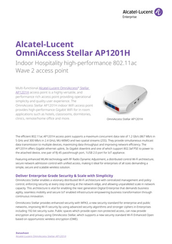
User's GuideSWRU359D – September 2013 – Revised March 2015WL1835MODCOM8B WLAN MIMO and Bluetooth ModuleEvaluation Board for TI Sitara PlatformThis user's guide describes how to use the TI WL1835MODCOM8B board to evaluate the performance ofthe TI WL18MODGB module.1234567ContentsIntroduction . 31.1Features . 41.2Applications . 51.3TI Module Key Benefits . 5Board Pin Assignment . 62.1Pin Descriptions . 7Electrical Characteristics . 9Antenna Characteristics. 94.1VSWR . 94.2Efficiency . 10Antenna Characteristics . 105.1Radio Pattern . 10Circuit Design . 146.1Schematic . 146.2Bill of Materials (BOM) . 15Layout Guidelines . 167.1Board Layout . 16List of Figures1WL1835MODCOM8B Top View . 32Board Top View . 63Board Bottom View . 64Antenna VSWR . 95Antenna Efficiency6Radio Pattern . 107ANT1 Polarization . 118ANT1 Polarization . 119ANT1 Polarization . 1210ANT2 Polarization . 1211ANT2 Polarization . 1312ANT2 Polarization . 1313Schematic . 1414Layer 1 . 1615Layer 2 . 1616Layer 3 . 17.10Sitara, WiLink8 are trademarks of Texas Instruments.Bluetooth is a registered trademark of Bluetooth SIG, Inc.Android is a trademark of Google Inc.Linux is a registered trademark of Linux Foundation.Wi-Fi is a registered trademark of Wi-Fi Alliance.SWRU359D – September 2013 – Revised March 2015Submit Documentation FeedbackWL1835MODCOM8B WLAN MIMO and Bluetooth Module Evaluation Boardfor TI Sitara PlatformCopyright 2013–2015, Texas Instruments Incorporated1
www.ti.com17Layer 4 . 1718Module Layout Guidelines (Top Layer) . 1819Module Layout Guidelines (Bottom Layer) . 1820Trace Design for the PCB Layout . 1921Layer 1 Combined With Layer 2. 1922Top Layer – Antenna and RF Trace Routing Layout Guidelines24.Bottom Layer – Antenna and RF Trace Routing Layout Guidelines.MIMO Antenna Spacing .1BOM . 152Module Layout Guidelines3Antenna and RF Trace Routing Layout Guidelines . 1923202021List of Tables.17WarningThe WL1835MODCOM8B board is tested to comply with ETSI/R&TTE over temperatures from –40 C to85 C.This board should not be modified to operate in other frequency bands other than what they are designedfor.FCC Licensing Requirements for the Wi-Fi and Bluetooth Radio Module of the EVM:For evaluation only; not FCC approved for resale. This kit is designed to allow:1. Product developers to evaluate electronic components, circuitry, or software associated with the kit todetermine whether to incorporate such items in a finished product2. Software developers to write software applications for use with the end product. This kit is not afinished product and when assembled may not be resold or otherwise marketed unless all requiredFCC equipment authorizations are first obtained. Operation is subject to the condition that this productnot cause harmful interference to licensed radio stations and that this product accept harmfulinterference. Unless the assembled kit is designed to operate under part 15, part 18, or part 95 of thischapter, the operator of the kit must operate under the authority of an FCC license holder or mustsecure an experimental authorization under part 5 of this chapter.Per TI’s Regulatory Compliance Information located in the WL1835ModCOMB8B User’s Guide’s“Evaluation Board/Kit/Module (EVM) Additional Terms,” this EVM cannot be used for production purposesand is explicitly restricted from end-product introduction.Use of this EVM requires the developer to provide a minimum distance of at least 20 cm from the antennato all persons in order to minimize risk of potential radiation hazards.CAUTIONDo not leave the EVM powered when unattended.2WL1835MODCOM8B WLAN MIMO and Bluetooth Module Evaluation Boardfor TI Sitara PlatformSWRU359D – September 2013 – Revised March 2015Submit Documentation FeedbackCopyright 2013–2015, Texas Instruments Incorporated
Introductionwww.ti.com1IntroductionThe WL1835MODCOM8B device is a Wi-Fi MIMO, Bluetooth, and Bluetooth Low Energy (BLE) moduleboard with the TI WL18MODGB module. WL18MODGB is built-in TI WL1835 IEEE 802.11 b/g/n andBluetooth 4.0 solutions to provide the best Wi-Fi and Bluetooth coexistence interoperability and powersaving technologies from TI.Figure 1. WL1835MODCOM8B Top ViewFCC/IC Regulatory ComplianceFCC Part 15 Class A CompliantIC ICES-003 Class A CompliantSWRU359D – September 2013 – Revised March 2015Submit Documentation FeedbackWL1835MODCOM8B WLAN MIMO and Bluetooth Module Evaluation Boardfor TI Sitara PlatformCopyright 2013–2015, Texas Instruments Incorporated3
Introductionwww.ti.com(continued)FCC ID: Z64-WL1835COMThis device complies with part 15 of theFCC Rules. Operation is subject to thefollowing two conditions: (1) This devicemay not cause harmful interference, and(2) this device must accept anyinterference received, includinginterference that may cause undesiredoperation.IC ID: 451I-WL1835COMThis device complies with IndustryCanada licence-exempt RSSstandard(s). Operation is subject to thefollowing two conditions: (1) this devicemay not cause interference, and (2) thisdevice must accept any interference,including that may cause undesiredoperation of the device.1.1Features 4WLAN, Bluetooth, BLE on a module board100-pin board cardDimension 76.0 mm(L) x 31.0 mm(W)WLAN 2.4 GHz SISO (20- and 40-MHz channels), 2.4-GHz MIMO (20-MHz channels)Support for BLE dual modeSeamless integration with TI Sitara and other application processorsDesign for TI AM335X general-purpose EVMWLAN and Bluetooth, BLE cores are software and hardware compatible with prior WL127x, WL128xand CC256x offerings, for smooth migration to device.Shared HCI transport for Bluetooth and BLE over UART and SDIO for WLAN.Wi-Fi / Bluetooth single antenna co-existenceBuilt-in chip antennaOptional U.FL RF connector for external 2.4-GHz band antennaDirect connection to battery using external switching mode power supply supporting 4.8-V to 2.9-VoperationVIO in the 1.8-V domainWL1835MODCOM8B WLAN MIMO and Bluetooth Module Evaluation Boardfor TI Sitara PlatformSWRU359D – September 2013 – Revised March 2015Submit Documentation FeedbackCopyright 2013–2015, Texas Instruments Incorporated
Introductionwww.ti.com1.2Applications 1.3Internet of Things MultimediaHome ElectronicsHome Appliances and White GoodsIndustrial and Home AutomationSmart Gateway and MeteringVideo ConferencingVideo Camera and SecurityTI Module Key Benefits Reduces Design Overhead: Single WiLink8 Module Scales Across Wi-Fi and Bluetooth.WLAN High Throughput: 80 Mbps (TCP), 100 Mbps (UDP)Bluetooth 4.0 BLE (Smart Ready)Wi-Fi-Bluetooth Single Antenna CoexistenceLow Power (30–50% Less than Previous Generation)Available as Easy-to-Use FCC, ETSI, and Telec Certified ModuleLower Manufacturing Costs, Saving Board Space and Minimizing RF ExpertiseAM335x Linux and Android Reference Platform Accelerates Customer Development and Time toMarketSWRU359D – September 2013 – Revised March 2015Submit Documentation FeedbackWL1835MODCOM8B WLAN MIMO and Bluetooth Module Evaluation Boardfor TI Sitara PlatformCopyright 2013–2015, Texas Instruments Incorporated5
Board Pin Assignment2www.ti.comBoard Pin AssignmentU1WL18MODGBFigure 2. Board Top ViewFigure 3. Board Bottom View6WL1835MODCOM8B WLAN MIMO and Bluetooth Module Evaluation Boardfor TI Sitara PlatformSWRU359D – September 2013 – Revised March 2015Submit Documentation FeedbackCopyright 2013–2015, Texas Instruments Incorporated
Board Pin Assignmentwww.ti.com2.1Pin DescriptionsNo.Name1SLOW CLKTypeIDescriptionSlow clock input2GNDGGround3GNDGGround4WL ENIWLAN Enable5VBATPPower supply input6GNDGGround7VBATPPower supply input8VIOPPower supply input for I/O pin9GNDGGround10N.C.11WL RS232 TX12N.C.13WL RS232 RX14N.C.15WL UART DBG16N.C.17N.C.18GNDGGround19GNDGGround20SDIO CLKIWLAN SDIO clock21N.C.22GND23N.C.24SDIO CMD25N.C.26SDIO D027N.C.28SDIO D129N.C.30SDIO D231N.C.32SDIO D333N.C.34WLAN IRQ35N.C.36N.C.37GND38N.C.No connection39N.C.No connection40N.C.No connection41N.C.42GND43N.C.No connection44N.C.No connection45N.C.No connection46N.C.47GNDNo connectionOWLAN tool RS232 outputNo connectionIWLAN tool RS232 inputNo connectionOWLAN Logger outputNo connectionNo connectionNo connectionGGroundNo connectionI/OWLAN SDIO commandNo connectionI/OWLAN SDIO data bit 0No connectionI/OWLAN SDIO data bit 1No connectionI/OWLAN SDIO data bit 2No connectionI/OWLAN SDIO data bit 3No connectionOWLAN SDIO interrupt outNo connectionNo connectionGGroundNo connectionGGroundNo connectionGSWRU359D – September 2013 – Revised March 2015Submit Documentation FeedbackGroundWL1835MODCOM8B WLAN MIMO and Bluetooth Module Evaluation Board forTI Sitara PlatformCopyright 2013–2015, Texas Instruments Incorporated7
Board Pin Assignment8www.ti.comNo.NameType48N.C.No connection49N.C.No connection50N.C.No connection51N.C.No connection52PCM IF CLK53N.C.54PCM IF FSYNC55N.C.56PCM IF DIN57N.C.58PCM IF d65N.C.66BT UART IF TX67N.C.68BT UART IF RX69N.C.70BT UART IF CTS71N.C.72BT UART IF RTS73N.C.74BT FUNC175N.C.76BT UART DEBUGOBluetooth Logger UART output77GNDGGround78GPIO9I/OGeneral-purpose I/O79N.C.No connection80N.C.No connection81N.C.No connection82N.C.83GND84N.C.No connection85N.C.No connection86N.C.87GND88N.C.89BT EN90N.C.No connection91N.C.No connection92GNDGGround93BT FUNC2IBT WAKE UP Bluetooth wakeup from host94N.C.95GNDGGround96GPIO11I/OGeneral-purpose I/OI/ODescriptionBluetooth PCM clock input or outputNo connectionI/OBluetooth PCM frame sync input or outputNo connectionIBluetooth PCM data inputNo connectionOBluetooth PCM data outputNo connectionGGroundNo connectionNo connectionNo connectionOBluetooth HCI UART transmit outputNo connectionIBluetooth HCI UART receive inputNo connectionIBluetooth HCI UART Clear to Send inputNo connectionOBluetooth HCI UART Request to Send outputNo connectionOBT HOST WAKE UP Signal to wake up the host from BluetoothNo connectionNo connectionGGroundNo connectionGGroundNo connectionIBluetooth EnableNo connectionWL1835MODCOM8B WLAN MIMO and Bluetooth Module Evaluation Board forTI Sitara PlatformSWRU359D – September 2013 – Revised March 2015Submit Documentation FeedbackCopyright 2013–2015, Texas Instruments Incorporated
Electrical GNDGGround98GPIO12I/OGeneral-purpose I/O99N.C.100GPIO10General-purpose I/OI/OGeneral-purpose I/OElectrical CharacteristicsRefer to the detailed data in the WL18MODGB data sheet (SWRS152) for electrical characteristics.4Antenna Characteristics4.1VSWRFigure 4 shows the antenna VSWR.Figure 4. Antenna VSWRSWRU359D – September 2013 – Revised March 2015Submit Documentation FeedbackWL1835MODCOM8B WLAN MIMO and Bluetooth Module Evaluation Boardfor TI Sitara PlatformCopyright 2013–2015, Texas Instruments Incorporated9
Antenna Characteristics4.2www.ti.comEfficiencyFigure 5 shows the antenna efficiency.Figure 5. Antenna Efficiency5Antenna Characteristics5.1Radio PatternFigure 6 shows the radio pattern of the WL1835MODCOM8B device.Figure 6. Radio Pattern10WL1835MODCOM8B WLAN MIMO and Bluetooth Module Evaluation Boardfor TI Sitara PlatformSWRU359D – September 2013 – Revised March 2015Submit Documentation FeedbackCopyright 2013–2015, Texas Instruments Incorporated
Antenna Characteristicswww.ti.com5.1.1ANT1Figure 7 shows the ANT1 polarization of the WL1835MODCOM8B device.Figure 7. ANT1 PolarizationFigure 8. ANT1 PolarizationSWRU359D – September 2013 – Revised March 2015Submit Documentation FeedbackWL1835MODCOM8B WLAN MIMO and Bluetooth Module Evaluation Boardfor TI Sitara PlatformCopyright 2013–2015, Texas Instruments Incorporated11
Antenna Characteristicswww.ti.comFigure 9. ANT1 Polarization5.1.2ANT2Figure 10 shows the ANT2 polarization of the WL1835MODCOM8B device.Figure 10. ANT2 Polarization12WL1835MODCOM8B WLAN MIMO and Bluetooth Module Evaluation Boardfor TI Sitara PlatformSWRU359D – September 2013 – Revised March 2015Submit Documentation FeedbackCopyright 2013–2015, Texas Instruments Incorporated
Antenna Characteristicswww.ti.comFigure 11. ANT2 PolarizationFigure 12. ANT2 PolarizationSWRU359D – September 2013 – Revised March 2015Submit Documentation FeedbackWL1835MODCOM8B WLAN MIMO and Bluetooth Module Evaluation Boardfor TI Sitara PlatformCopyright 2013–2015, Texas Instruments Incorporated13
Circuit Designwww.ti.com6.1SchematicWLAN EN SOCBT EN SOCWL UART DBGR10R 0402R20R 0402R4BT UART DBGR3J1HEADER 1x2H-1X2 2MM0R 040221Circuit DesignTP21TP110R 0402VBAT IN1TP8VIO INC210uF0603C11uF0402R320R0402C30.1uF0402SLOW 28291TP32930281TP43132343SLOW CLKR60R04022OUTGNDENVCCVIO INVBAT IN14C40.1uF0402WL RS232 TXWL RS232 RXGND2G4 ANT2 NDGND2G4 ANT1 WBThese two TPs for test modewhen WL IRQ pull high.R120R0402WL RS232 TX33R130R0402WL RS232 RX3536373824394023414222R170R0402BT FUNC2434421R190R0402BT 566676869707172737475767778798081822726251TP5182G4 ANT2 HEADER 1x2H-1X2 2MMShort PIN Header (1-2)for entering test mode.Open for function mode.WLAN EN SOCVIO INSDIO CLK WLSDIO CMD WLSDIO D0 WLSDIO D1 WLSDIO D2 WLSDIO D3 WLR100R0402WLAN IRQBT AUD CLKBT AUD FSYNCBT AUD INBT AUD OUTBT HCI TXBT HCI RXBT HCI CTSBT HCI RTSBT FUNC1BT UART DGNDGNDGNDGNDGNDGNDGNDGNDWLAN IRQGND3212343533GNDGNDGND363738VIOGNDEXT 32K4140434239GNDWLAN EN SOCBT EN SOCBT UART DBGWL UART 29G30G31G32G33G34G35G36GNDRESERVED31464GNDWL SDIO D363RESERVED1WL SDIO D2621GNDRESERVED2WL SDIO D1TP6GNDBT AUD CLK1361GPIO 4GND12600R 0402BT AUD FSYNC11R18BT AUD OUTWL SDIO D059BT AUD CLKU1WL1835MODGBE-13.4X13.3-N100 0.75-TOPBT AUD INGND589570R 0402GPIO 2100R 0402R16GNDWL SDIO CLKR15BT AUD FSYNCGPIO 1GNDBT AUD OUTGNDWL SDIO CMD56GND80R 0402BT HCI RX7R14GND655BT AUD INBT HCI TXGPIO1254GNDGPIO10530402BT HCI CTS5520RVBATGND0R 0402R11GNDGPIO9R9BT HCI RX2G4 ANT1 WBBT HCI RTSGPIO11BT HCI TXGNDGND514500R 040230R 0402R82R7BT HCI CTSVBAT4847WL UART DBGBT HCI RTSNU 0R04023OSC11V8 / 32.768kHzOSC-3.2X2.5J3HEADER 1x2H-1X2 2MM49R51R310R0402216VIO IN8384GPIO11R210R 0402WLAN IRQ8586GPIO9R220R 0402R230R0402SDIO D3 WL8788GPIO10R240R 0402R250R0402SDIO D2 WL8990GPIO12R260R 0402R270R0402SDIO D1 WL9192R290R0402SDIO D0 WL9394R300R0402SDIO CLK WL9596R280R0402SDIO CMD WL979899100R2010k0402BT EN SOCBT FUNC2GPIO11GPIO12GPIO10J2NU 100pin Micro Edge MEC6SD-100PEDGE CONNECTOR - MALEWL BG 1ANT-N3-1.6X0.8MM-BAFEEDC92pF04022.4G5GB2C7NU 10pF0402C610pF04022G4 ANT2 WA2G4 ANT1 WBC8NU 10pF0402C10NU pF0402B1C510pF0402B1WL BG/BT e 13. Schematic14WL1835MODCOM8B WLAN MIMO and Bluetooth Module Evaluation Board forTI Sitara PlatformCopyright 2013–2015, Texas Instruments IncorporatedSWRU359D – September 2013 – Revised March 2015Submit Documentation Feedback
Circuit Designwww.ti.com6.2Bill of Materials (BOM)Table 1 lists the bill of materials.Table 1. BOM1TI WL1835 Wi-Fi/Bluetooth ModuleWL18MODGBU12XOSC 3225 / 32.768 kHz / 1.8 V / 50 ppm7XZ3200005OSC13ANT / Chip / 2.4 GHz, 5 GHz / Peak Gain 5 dBiANT016008LCD2442MA1ANT1, ANT24CON Male 1x2 / PitchP301-SGP-040/028-02J1, J3, J45DC JUMPER / PITCH 2.0 mmCMJ-20BBJ1, J36Mini RF Header ReceptacleU.FL-R-SMT-1(10)J5, J67IND 0402 / 1.1 nH / 0.05 nH / SMDLQP15MN1N1W02L18IND 0402 / 1.5 nH / 0.05 nH / SMDLQP15MN1N5W02L29CAP 0402 / 1.2 pF / 50 V / C0G / 0.1 pFGJM1555C1H1R2BB01C1110CAP 0402 / 2.2 pF / 50 V / C0G / 0.1 pFGJM1555C1H2R2BB01C911CAP 0402 / 4 pF / 50 V / C0G / 0.1 pFGJM1555C1H4R0BB01C1412CAP 0402 / 8 pF / 50 V / C0G / 0.1 pFGJM1555C1H8R0BB01C1313CAP 0402 / 10 pF / 50 V / NPO / 5%0402N100J500LTC7, C814CAP 0402 / 0.1 µF / 6.3 V / X7R / 10%0402B104K100CTC3, C415CAP 0402 / 1 µF / 6.3 V / X5R / 10% / HFGRM155R60J105KE19DC116CAP 0603 / 10 µF / 6.3 V / X5R / 20%C1608X5R0J106MC217RES 0402 / 0R / 5%WR04X000 PTLR1, R2, R3, R4, R5, R6, R7, R8, R9,R10, R11, R12, R13, R14, R15,R16, R17, R18, R19, R21, R22,R23, R24, R25, R26, R27, R28,R29, R30, R31, R3218RES 0402 / 10K / 5%WR04X103 JTLR20SWRU359D – September 2013 – Revised March 2015Submit Documentation FeedbackWL1835MODCOM8B WLAN MIMO and Bluetooth Module Evaluation Boardfor TI Sitara PlatformCopyright 2013–2015, Texas Instruments Incorporated15
Layout Guidelines7Layout Guidelines7.1Board Layoutwww.ti.comFigure 14 shows the WL1835MODCOM8B 4-layer board. Table 2, Figure 15, Figure 16, Figure 17,Figure 18, and Figure 19 show instances of good layout practices.Figure 14. Layer 1Figure 15. Layer 216WL1835MODCOM8B WLAN MIMO and Bluetooth Module Evaluation Boardfor TI Sitara PlatformSWRU359D – September 2013 – Revised March 2015Submit Documentation FeedbackCopyright 2013–2015, Texas Instruments Incorporated
Layout Guidelineswww.ti.comFigure 16. Layer 3Figure 17. Layer 4Table 2. Module Layout GuidelinesReferenceGuideline Description1The proximity of ground vias must be close to the pad.2Signal traces must not be run underneath the module on the layer where the module is mounted.3Have a complete ground pour in layer 2 for thermal dissipation.4Have a solid ground plane and ground vias under the module for stable system and thermal dissipation.5Increase the ground pour in the first layer and have all of the traces from the first layer on the inner layers, ifpossible.6Signal traces can be run on a third layer under the solid ground layer, which is below the module mountinglayer.SWRU359D – September 2013 – Revised March 2015Submit Documentation FeedbackWL1835MODCOM8B WLAN MIMO and Bluetooth Module Evaluation Boardfor TI Sitara PlatformCopyright 2013–2015, Texas Instruments Incorporated17
Layout Guidelineswww.ti.comFigure 18. Module Layout Guidelines (Top Layer)Figure 19. Module Layout Guidelines (Bottom Layer)Figure 20 shows the trace design for the PCB. A 50-Ω impedance match on the trace to the antennashould be used. Also, 50-Ω traces are recommended for the PCB layout.18WL1835MODCOM8B WLAN MIMO and Bluetooth Module Evaluation Boardfor TI Sitara PlatformSWRU359D – September 2013 – Revised March 2015Submit Documentation FeedbackCopyright 2013–2015, Texas Instruments Incorporated
Layout Guidelineswww.ti.comFigure 20. Trace Design for the PCB LayoutFigure 21 shows layer 1 with the trace to the antenna over ground layer 2.Figure 21. Layer 1 Combined With Layer 2Table 3, Figure 22, and Figure 23 describe instances of good layout practices for the antenna and RFtrace routing.Table 3. Antenna and RF Trace Routing Layout GuidelinesReferenceGuideline Description1The RF trace antenna feed must be as short as possible beyond the ground reference. At this point, the tracestarts to radiate.2The RF trace bends must be gradual with an approximate maximum bend of 45 degrees with trace mitered. RFtraces must not have sharp corners.3RF traces must have via stitching on the ground plane beside the RF trace on both sides4RF traces must have constant impedance (microstrip transmission line).5For best results, the RF trace ground layer must be the ground layer immediately below the RF trace. Theground layer must be solid.6There must be no traces or ground under the antenna section.7RF traces must be as short as possible. The antenna, RF traces, and modules must be on the edge of the PCBproduct. The proximity of the antenna to the enclosure and the enclosure material must also be considered.SWRU359D – September 2013 – Revised March 2015Submit Documentation FeedbackWL1835MODCOM8B WLAN MIMO and Bluetooth Module Evaluation Boardfor TI Sitara PlatformCopyright 2013–2015, Texas Instruments Incorporated19
Layout Guidelineswww.ti.comFigure 22. Top Layer – Antenna and RF Trace Routing Layout GuidelinesFigure 23. Bottom Layer – Antenna and RF Trace Routing Layout Guidelines20WL1835MODCOM8B WLAN MIMO and Bluetooth Module Evaluation Boardfor TI Sitara PlatformSWRU359D – September 2013 – Revised March 2015Submit Documentation FeedbackCopyright 2013–2015, Texas Instruments Incorporated
Layout Guidelineswww.ti.comFigure 24 describes the MIMO antenna spacing. The distance of ANT1 and ANT2 must be greater thanhalf of wavelength (62.5 mm at 2.4 GHz).Figure 24. MIMO Antenna SpacingThe supply routing guidelines are as follows: For power supply routing, the power trace for VBAT must be at least 40-mil wide. The 1.8-V trace must be at least 18-mil wide. Make VBAT traces as wide as possible to ensure reduced inductance and trace resistance. If possible, shield VBAT traces with ground above, below, and beside the traces.The digital signals routing guidelines are as follows: SDIO signals traces (CLK, CMD, D0, D1, D2, and D3) should be routed in parallel to each other andas short as possible (less than 12 cm). In addition, every trace length must be the same as the others.There should be enough space between traces – greater than 1.5 times the trace width or ground – toensure signal quality, especially for the SDIO CLK trace. Remember to keep them away from theother digital or analog signal traces. TI recommends adding ground shielding around these buses. SDIO Clock, PCM clock These digital clock signals are a source of noise. Keep the traces of thesesignals as short as possible. Whenever possible, maintain a clearance around them.SWRU359D – September 2013 – Revised March 2015Submit Documentation FeedbackWL1835MODCOM8B WLAN MIMO and Bluetooth Module Evaluation Boardfor TI Sitara PlatformCopyright 2013–2015, Texas Instruments Incorporated21
Revision Historywww.ti.comThis user's guide revision history highlights the technical changes made to the SWRU359 device-specific user'sguide.Revision HistoryRevisionDateSWRS359CJanuary 2014SWRS359DMarch 2015Description / ChangesChanged all references of the module fromWL1835MODGB to WL18MODGB.In : Changed tested-temperature range from 0 – 70, to–20 – 70.Changed supply routing guidelines from 40-mm to 40-mil,18-mm to 18-milReformatted sections22Revision HistorySWRU359D – September 2013 – Revised March 2015Submit Documentation FeedbackCopyright 2013–2015, Texas Instruments Incorporated
IMPORTANT NOTICETexas Instruments Incorporated and its subsidiaries (TI) reserve the right to make corrections, enhancements, improvements and otherchanges to its semiconductor products and services per JESD46, latest issue, and to discontinue any product or service per JESD48, latestissue. Buyers should obtain the latest relevant information before placing orders and should verify that such information is current andcomplete. All semiconductor products (also referred to herein as “components”) are sold subject to TI’s terms and conditions of salesupplied at the time of order acknowledgment.TI warrants performance of its components to the specifications applicable at the time of sale, in accordance with the warranty in TI’s termsand conditions of sale of semiconductor products. Testing and other quality control techniques are used to the extent TI deems necessaryto support this warranty. Except where mandated by applicable law, testing of all parameters of each component is not necessarilyperformed.TI assumes no liability for applications assistance or the design of Buyers’ products. Buyers are responsible for their products andapplications using TI components. To minimize the risks associated with Buyers’ products and applications, Buyers should provideadequate design and operating safeguards.TI does not warrant or represent that any license, either express or implied, is granted under any patent right, copyright, mask work right, orother intellectual property right relating to any combination, machine, or process in which TI components or services are used. Informationpublished by TI regarding third-party products or services does not constitute a license to use such products or services or a warranty orendorsement thereof. Use of such information may require a license from a third party under the patents or other intellectual property of thethird party, or a license from TI under the patents or other intellectual property of TI.Reproduction of significant portions of TI information in TI data books or data sheets is permissible only if reproduction is without alterationand is accompanied by all associated warranties, conditions, limitations, and notices. TI is not responsible or liable for such altereddocumentation. Information of third parties may be subject to additional restrictions.Resale of TI components or services with statements different from or beyond the parameters stated by TI for that component or servicevoids all express and any implied warranties for the associated TI component or service and is an unfair and deceptive business practice.TI is not responsible or liable for any such statements.Buyer acknowledges and agrees that it is solely responsible for compliance with all legal, regulatory and safety-related requirementsconcerning its products, and any use of TI components in its applications, notwithstanding any applications-related information or supportthat may be provided by TI. Buyer represents and agrees that it has all the necessary expertise to create and implement safeguards whichanticipate dangerous consequences of failures, monitor failures and their consequences, lessen the likelihood of failures that might causeharm and take appropriate remedial action
Video Conferencing Video Camera and Security 1.3 TI Module Key Benefits . 74 BT_FUNC1 O BT_HOST_WAKE_UP Signal to wake up the host from Bluetooth 75 N.C. No connection 76 BT_UART_DEBUG O Bluetooth Logger UART output 77 GND G Ground 78 GPIO9 I/O General-purpose I/O 79 N.C. No connection


![[MS-CDP-Diff]: Connected Devices Platform Protocol Version 3](/img/35/5bms-cdp-5d-220429-diff.jpg)