Transcription
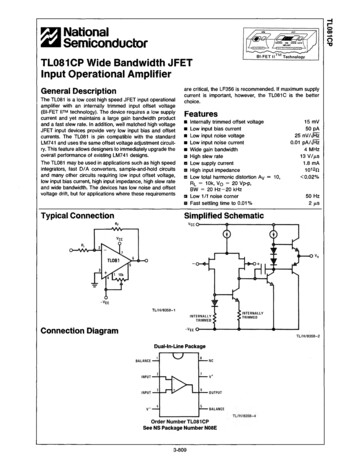
TL081 Wide Bandwidth JFETInput Operational AmplifierGeneral DescriptionThe TL081 is a low cost high speed JFET input operationalamplifier with an internally trimmed input offset voltage(BI-FET IITM technology). The device requires a low supplycurrent and yet maintains a large gain bandwidth productand a fast slew rate. In addition, well matched high voltageJFET input devices provide very low input bias and offsetcurrents. The TL081 is pin compatible with the standardLM741 and uses the same offset voltage adjustment circuitry. This feature allows designers to immediately upgrade theoverall performance of existing LM741 designs.The TL081 may be used in applications such as high speedintegrators, fast D/A converters, sample-and-hold circuitsand many other circuits requiring low input offset voltage,low input bias current, high input impedance, high slew rateand wide bandwidth. The devices has low noise and offsetvoltage drift, but for applications where these requirementsare critical, the LF356 is recommended. If maximum supplycurrent is important, however, the TL081C is the betterchoice.FeaturesYYYYYYYYYYYInternally trimmed offset voltageLow input bias currentLow input noise voltageLow input noise currentWide gain bandwidthHigh slew rateLow supply currentHigh input impedanceLow total harmonic distortion AV e 10,RL e 10k, VO e 20 Vp-p,BW e 20 Hzb20 kHzLow 1/f noise cornerFast settling time to 0.01%15 mV50 pA25 nV/0Hz0.01 pA/0Hz4 MHz13 V/ms1.8 mA1012Xk 0.02%50 Hz2 msSimplified SchematicTypical ConnectionTL/H/8358 – 1Connection DiagramTL/H/8358 – 2Dual-In-Line PackageTL/H/8358 – 4Order Number TL081CPSee NS Package Number N08EBI-FET IITM is a trademark of National Semiconductor Corp.C1995 National Semiconductor CorporationTL/H/8358RRD-B30M125/Printed in U. S. A.TL081 Wide Bandwidth JFET Input Operational AmplifierDecember 1995
Absolute Maximum RatingsIf Military/Aerospace specified devices are required,please contact the National Semiconductor SalesOffice/Distributors for availability and specifications.Supply Voltageg 18VPower Dissipation (Notes 1 and 6)Operating Temperature RangeTj(MAX)Differential Input VoltageInput Voltage Range (Note 2)g 15VOutput Short Circuit DurationContinuousStorage Temperature Rangeb 65§ C to a 150§ CLead Temp. (Soldering, 10 seconds)ijA670 mW0§ C to a 70§ C115§ Cg 30V260§ C120§ C/WESD rating to be determined.DC Electrical Characteristics (Note 20VOSInput Offset VoltageRS e 10 kX, TA e 25§ COver TemperatureDVOS/DTAverage TC of Input OffsetVoltageRS e 10 kXIOSInput Offset CurrentTj e 25§ C, (Notes 3, 4)Tj s 70§ C251004pAnAIBInput Bias CurrentTj e 25§ C, (Notes 3, 4)Tj s 70§ C502008pAnARINInput ResistanceTj e 25§ CLarge Signal Voltage GainVS e g 15V, TA e 25§ CVO e g 10V, RL e 2 kX25Over Temperature15AVOLVOOutput Voltage SwingVCMInput Common-Mode VoltageRangeCMRRVS e g 15V, RL e 10 kX10mVmVmV/§ C1012X100V/mVV/mVg 12g 13.5VVS e g 15Vg 11a 15b 12VVCommon-Mode Rejection RatioRS s 10 kX70100dBPSRRSupply Voltage Rejection Ratio(Note 5)70100ISSupply Current1.8dB2.8mAAC Electrical Characteristics (Note lew RateVS e g 15V, TA e 25§ C13V/msGBWGain Bandwidth ProductVS e g 15V, TA e 25§ C4MHzenEquivalent Input Noise VoltageTA e 25§ C, RS e 100X,f e 1000 Hz25nV/0HzinEquivalent Input Noise CurrentTj e 25§ C, f e 1000 Hz0.01pA/0HzNote 1: For operating at elevated temperature, the device must be derated based on a thermal resistance of 120§ C/W junction to ambient for N package.Note 2: Unless otherwise specified the absolute maximum negative input voltage is equal to the negative power supply voltage.Note 3: These specifications apply for VS e g 15V and 0§ C s TA s a 70§ C. VOS, IB and IOS are measured at VCM e 0.Note 4: The input bias currents are junction leakage currents which approximately double for every 10§ C increase in the junction temperature, Tj. Due to the limitedproduction test time, the input bias currents measured are correlated to junction temperature. In normal operation the junction temperature rises above the ambienttemperature as a result of internal power dissipation, PD. Tj e TA a ijA PD where ijA is the thermal resistance from junction to ambient. Use of a heat sink isrecommended if input bias current is to be kept to a minimum.Note 5: Supply voltage rejection ratio is measured for both supply magnitudes increasing or decreasing simultaneously in accordance with common practice fromVS e g 5V to g 15V.Note 6: Max. Power Dissipation is defined by the package characteristics. Operating the part near the Max. Power Dissipation may cause the part to operateoutside guaranteed limits.2
Typical Performance CharacteristicsInput Bias CurrentInput Bias CurrentSupply CurrentPositive Common-Mode InputVoltage LimitNegative Common-Mode InputVoltage LimitPositive Current LimitNegative Current LimitVoltage SwingOutput Voltage SwingGain BandwidthBode PlotSlew RateTL/H/8358 – 53
Typical Performance CharacteristicsDistortion vs Frequency(Continued)Undistorted Output VoltageSwingCommon-Mode RejectionRatioPower Supply RejectionRatioOpen Loop Voltage Gain (V/V)Output ImpedanceOpen Loop FrequencyResponseEquivalent Input NoiseVoltageInverter Settling TimeTL/H/8358 – 64
Pulse ResponseSmall Signal InvertingSmall Signal Non-InvertingTL/H/8358 – 7TL/H/8358 – 13Large Signal InvertingLarge Signal Non-InvertingTL/H/8358 – 14TL/H/8358 – 15Current Limit (RL e 100X)TL/H/8358 – 16Application Hintswill cause large currents to flow which can result in a destroyed unit.Exceeding the negative common-mode limit on either inputwill force the output to a high state, potentially causing areversal of phase to the output.Exceeding the negative common-mode limit on both inputswill force the amplifier output to a high state. In neither casedoes a latch occur since raising the input back within theThe TL081 is an op amp with an internally trimmed inputoffset voltage and JFET input devices (BI-FET II). TheseJFETs have large reverse breakdown voltages from gate tosource and drain eliminating the need for clamps across theinputs. Therefore, large differential input voltages can easilybe accommodated without a large increase in input current.The maximum differential input voltage is independent ofthe supply voltages. However, neither of the input voltagesshould be allowed to exceed the negative supply as this5
Application Hints (Continued)resulting forward diode within the IC could cause fusing ofthe internal conductors and result in a destroyed unit.common-mode range again puts the input stage and thusthe amplifier in a normal operating mode.Exceeding the positive common-mode limit on a single inputwill not change the phase of the output; however, if bothinputs exceed the limit, the output of the amplifier will beforced to a high state.The amplifier will operate with a common-mode input voltage equal to the positive supply; however, the gain bandwidth and slew rate may be decreased in this condition.When the negative common-mode voltage swings to within3V of the negative supply, an increase in input offset voltagemay occur.The TL081 is biased by a zener reference which allows normal circuit operation on g 4V power supplies. Supply voltages less than these may result in lower gain bandwidth andslew rate.The TL081 will drive a 2 kX load resistance to g 10V overthe full temperature range of 0§ C to a 70§ C. If the amplifieris forced to drive heavier load currents, however, an increase in input offset voltage may occur on the negativevoltage swing and finally reach an active current limit onboth positive and negative swings.Precautions should be taken to ensure that the power supply for the integrated circuit never becomes reversed in polarity or that the unit is not inadvertently installed backwardsin a socket as an unlimited current surge through theBecause these amplifiers are JFET rather than MOSFETinput op amps they do not require special handling.As with most amplifiers, care should be taken with leaddress, component placement and supply decoupling in order to ensure stability. For example, resistors from the output to an input should be placed with the body close to theinput to minimize ‘‘pick-up’’ and maximize the frequency ofthe feedback pole by minimizing the capacitance from theinput to ground.A feedback pole is created when the feedback around anyamplifier is resistive. The parallel resistance and capacitance from the input of the device (usually the inverting input) to AC ground set the frequency of the pole. In manyinstances the frequency of this pole is much greater thanthe expected 3 dB frequency of the closed loop gain andconsequently there is negligible effect on stability margin.However, if the feedback pole is less than approximately 6times the expected 3 dB frequency a lead capacitor shouldbe placed from the output to the input of the op amp. Thevalue of the added capacitor should be such that the RCtime constant of this capacitor and the resistance it parallelsis greater than or equal to the original feedback pole timeconstant.Detailed SchematicTL/H/8358 – 86
Typical ApplicationsSupply Current Indicator/LimiterHi-ZIN Inverting AmplifierTL/H/8358 – 9TL/H/8358 – 10# VOUT switches high when RSIS l VDParasitic input capacitance C1 j (3 pF for TL081 plus any additionallayout capacitance) interacts with feedback elements and creates undesirable high frequency pole. To compensate, add C2 such that:R2C2 j R1C1.Ultra-Low (or High) Duty Cycle PulseGeneratorLong Time IntegratorTL/H/8358–11# tOUTPUT HIGH & R1C fin4.8 b 2VS4.8 b VSTL/H/8358 – 12* Low leakage capacitor2V b 7.8# tOUTPUT LOW & R2C fin SVS b 7.8# 50k pot used for less sensitive VOS adjustwhere VS e V a a l Vb l*low leakage capacitor7
TL081 Wide Bandwidth JFET Input Operational AmplifierPhysical Dimensions inches (millimeters)Molded Dual-In-Line Package (N)Order Number TL081CPNS Package Number N08ELIFE SUPPORT POLICYNATIONAL’S PRODUCTS ARE NOT AUTHORIZED FOR USE AS CRITICAL COMPONENTS IN LIFE SUPPORTDEVICES OR SYSTEMS WITHOUT THE EXPRESS WRITTEN APPROVAL OF THE PRESIDENT OF NATIONALSEMICONDUCTOR CORPORATION. As used herein:1. Life support devices or systems are devices orsystems which, (a) are intended for surgical implantinto the body, or (b) support or sustain life, and whosefailure to perform, when properly used in accordancewith instructions for use provided in the labeling, canbe reasonably expected to result in a significant injuryto the user.National SemiconductorCorporation1111 West Bardin RoadArlington, TX 76017Tel: 1(800) 272-9959Fax: 1(800) 737-70182. A critical component is any component of a lifesupport device or system whose failure to perform canbe reasonably expected to cause the failure of the lifesupport device or system, or to affect its safety oreffectiveness.National SemiconductorEuropeFax: (a49) 0-180-530 85 86Email: cnjwge @ tevm2.nsc.comDeutsch Tel: (a49) 0-180-530 85 85English Tel: (a49) 0-180-532 78 32Fran3ais Tel: (a49) 0-180-532 93 58Italiano Tel: (a49) 0-180-534 16 80National SemiconductorHong Kong Ltd.13th Floor, Straight Block,Ocean Centre, 5 Canton Rd.Tsimshatsui, KowloonHong KongTel: (852) 2737-1600Fax: (852) 2736-9960National SemiconductorJapan Ltd.Tel: 81-043-299-2309Fax: 81-043-299-2408National does not assume any responsibility for use of any circuitry described, no circuit patent licenses are implied and National reserves the right at any time without notice to change said circuitry and specifications.
The TL081 is biased by a zener reference which allows nor-mal circuit operation on g4V power supplies. Supply volt-ages less than these may result in lower gain bandwidth and slew rate. The TL081 will drivea2kXload resistance to g10V over the full temperature range of 0§Ctoa70§C. If the amplifier is forced to drive heavier load currents .