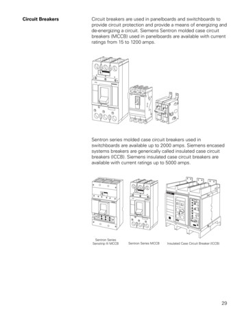
Transcription
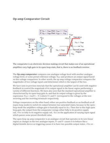
Op-amp Comparator CircuitThe comparator is an electronic decision making circuit that makes use of an operationalamplifiers very high gain in its open-loop state, that is, there is no feedback resistor.The Op-amp comparator compares one analogue voltage level with another analoguevoltage level, or some preset reference voltage, VREF and produces an output signal basedon this voltage comparison. In other words, the op-amp voltage comparator compares themagnitudes of two voltage inputs and determines which is the largest of the two.We have seen in previous tutorials that the operational amplifier can be used with negativefeedback to control the magnitude of its output signal in the linear region performing avariety of different functions. We have also seen that the standard operational amplifier ischaracterised by its open-loop gain AO and that its output voltage is given by theexpression: VOUT AO(V – V-) where V and V- correspond to the voltages at the noninverting and the inverting terminals respectively.Voltage comparators on the other hand, either use positive feedback or no feedback at all(open-loop mode) to switch its output between two saturated states, because in the openloop mode the amplifiers voltage gain is basically equal to AVO. Then due to this high openloop gain, the output from the comparator swings either fully to its positive supplyrail, Vcc or fully to its negative supply rail, -Vcc on the application of varying input signalwhich passes some preset threshold value.The open-loop op-amp comparator is an analogue circuit that operates in its non-linearregion as changes in the two analogue inputs, V and V- causes it to behave like adigital bistable device as triggering causes it to have two possible output states, Vcc or -
Vcc. Then we can say that the voltage comparator is essentially a 1-bit analogue to digitalconverter, as the input signal is analogue but the output behaves digitally.With reference to the op-amp comparator circuit above, lets first assume that VIN is lessthan the DC voltage level at VREF, ( VIN VREF ). As the non-inverting (positive) input of thecomparator is less than the inverting (negative) input, the output will be LOW and at thenegative supply voltage, -Vcc resulting in a negative saturation of the output.If we now increase the input voltage, VIN so that its value is greater than the referencevoltage VREF on the inverting input, the output voltage rapidly switches HIGH towards thepositive supply voltage, Vcc resulting in a positive saturation of the output. If we reduceagain the input voltage VIN, so that it is slightly less than the reference voltage, the op-amp’soutput switches back to its negative saturation voltage acting as a threshold detector.Then we can see that the op-amp voltage comparator is a device whose output isdependant on the value of the input voltage, VIN with respect to some DC voltage level asthe output is HIGH when the voltage on the non-inverting input is greater than the voltageon the inverting input, and LOW when the non-inverting input is less than the invertinginput voltage. This condition is true regardless of whether the input signal is connected tothe inverting or the non-inverting input of the comparator.We can also see that the value of the output voltage is completely dependent on the opamps power supply voltage. In theory due to the op-amps high open-loop gain themagnitude of its output voltage could be infinite in both directions, ( ). Howeverpractically, and for obvious reasons it is limited by the op-amps supply railsgiving VOUT Vcc or VOUT -Vcc.We said before that the basic op-amp comparator produces a positive or negative voltageoutput by comparing its input voltage against some preset DC reference voltage. Generally,a resistive voltage divider is used to set the input reference voltage of a comparator, but abattery source, zener diode or potentiometer for a variable reference voltage can all beused as shown.Comparator Reference Voltages
In theory the comparators reference voltage can be set to be anywhere between 0v and thesupply voltage but there are practical limitations on the actual voltage range depending onthe op-amp comparator being device used.Positive and Negative Voltage ComparatorsA basic op-amp comparator circuit can be used to detect either a positive or a negativegoing input voltage depending upon which input of the operational amplifier we connectthe fixed reference voltage source and the input voltage too. In the examples above we haveused the inverting input to set the reference voltage with the input voltage connected to thenon-inverting input.But equally we could connect the inputs of the comparator the other way around invertingthe output signal to that shown above. Then an op-amp comparator can be configured tooperate in what is called an inverting or a non-inverting configuration.Positive Voltage ComparatorThe basic configuration for the positive voltage comparator, also known as a non-invertingcomparator circuit detects when the input signal, VIN is ABOVE or more positive than thereference voltage, VREF producing an output at VOUT which is HIGH as shown.Non-inverting Comparator CircuitIn this non-inverting configuration, the reference voltage is connected to the invertinginput of the operational amplifier with the input signal connected to the non-invertinginput. To keep things simple, we have assumed that the two resistors forming the potentialdivider network are equal and: R1 R2 R. This will produce a fixed reference voltagewhich is one half that of the supply voltage, that is Vcc/2, while the input voltage is variablefrom zero to the supply voltage.
When VIN is greater than VREF, the op-amp comparators output will saturate towards thepositive supply rail, Vcc. When VIN is less than VREF the op-amp comparators output willchange state and saturate at the negative supply rail, 0v as shown.Negative Voltage ComparatorThe basic configuration for the negative voltage comparator, also known as an invertingcomparator circuit detects when the input signal, VIN is BELOW or more negative than thereference voltage, VREF producing an output at VOUT which is HIGH as shown.Inverting Comparator CircuitIn the inverting configuration, which is the opposite of the positive configuration above, thereference voltage is connected to the non-inverting input of the operational amplifier whilethe input signal is connected to the inverting input. Then when VIN is less than VREF the opamp comparators output will saturate towards the positive supply rail, Vcc.Likewise the reverse is true, when VIN is greater than VREF, the op-amp comparators outputwill change state and saturate towards the negative supply rail, 0v.Then depending upon which op-amp inputs we use for the signal and the reference voltage,we can produce an inverting or non-inverting output. We can take this idea of detectingeither a negative or positive going signal one step further by combining the two op-ampcomparator circuits above to produce a window comparator circuit.Window ComparatorA Window Comparator is basically the inverting and the non-inverting comparatorsabove combined into a single comparator stage. The window comparator detects inputvoltage levels that are within a specific band or window of voltages, instead of indicatingwhether a voltage is greater or less than some preset or fixed voltage reference point.
This time, instead of having just one reference voltage value, a window comparator willhave two reference voltages implemented by a pair of voltage comparators. One whichtriggers an op-amp comparator on detection of some upper voltagethreshold, VREF(UPPER) and one which triggers an op-amp comparator on detection of a lowervoltage threshold level, VREF(LOWER). Then the voltage levels between these two upper andlower reference voltages is called the “window”, hence its name.Using our idea above of a voltage divider network, if we now use three equal value resistorsso that R1 R2 R3 R we can create a very simple window comparator circuit as shown.Also as the resistive values are all equal, the voltage drops across each resistor will also beequal at one-third the supply voltage, 1/3Vcc. So for ease in this simple windowcomparator example, we can set the upper reference voltage to 2/3Vcc and the lowerreference voltage to 1/3Vcc.Consider the window comparator circuit below.Window Comparator CircuitThe inital switching condition of the circuit is the open-collector output of op-amp A1 “OFF”with the open-collector output of op-amp A2, “ON” (sinking current) so VOUT is equal to 0V.When VIN is below the lower voltage level, VREF(LOWER) which equates to 1/3Vcc, VOUT will beLOW. When VIN exceeds this 1/3Vcc lower voltage level, the first op-amp comparatordetects this and switches its open-collector output HIGH. This means that both op-ampshave their outputs HIGH at the same time. No current flows through the pull-upresistor RL so VOUT is equal to Vcc.As VIN continues to increase it passes the upper voltage level, VREF(UPPER) at 2/3Vcc. At thispoint the second op-amp comparator detects this and switches its output LOW andVOUT becomes equal to 0V.
Then the difference between VREF(UPPER) and VREF(LOWER) (which is 2/3Vccc – 1/3Vcc in thisexample) creates the switching window for the positive going signal.Lets now assume that VIN is at its maximum value and equal to Vcc. As VIN decreases itpasses the upper voltage level VREF(UPPER) of the second op-amp comparator which switchesthe output HIGH. As VIN continues to decrease it passes the lower voltagelevel, VREF(LOWER) of the first op-amp comparator once again switching the output LOW.Then the difference between VREF(UPPER) and VREF(LOWER) creates the window for the negativegoing signal. So we can see that as VIN passes above or passes below the upper and lowerreference levels set by the two op-amp comparators, the output signal VOUT will be HIGH orLOW.In this simple example we have set the upper trip level at 2/3Vcc and the lower trip level at1/3Vcc (because we used three equal value resistors), but can be any values we choose byadjusting the input thresholds. As a result, the window width can be customized for a givenapplication.If we used a dual power supply and set the upper and lower trip levels to say 10 voltsand VIN was a sinusoidal waveform, then we could use this window comparator circuit as azero crossing detector of the sine wave which would produce an output, HIGH or LOWevery time the sine wave crossed the zero volts line from positive to negative or negative topositive.We can take this idea of detecting voltage levels further by connecting a number ofdifferent op-amp comparators together with them all using a common input signal, butwith each comparator using a different reference voltage set by our now familiar voltagedivider network across the supply. Consider the voltage level detector circuit below.Comparator Voltage Level Detector
As above, the voltage divider network provides a set of reference voltages for the individualop-amp comparator circuits. To produce the four reference voltages will require fiveresistors. The junction at the bottom pair of resistors will produce a reference voltage thatis one-fifth the supply voltage, 1/5Vcc using equal value resistors. The second pair 2/5Vcc,a third pair 3/5Vcc and so on, with these reference voltages increasing by a fixed amount ofone-fifth (1/5) towards 5/5Vcc which is actually Vcc.As the common input voltage increases, the output of each op-amp comparator circuitswitches in turn thereby turning OFF the connected LED starting with the lowercomparator, A4 and upwards towards A1 as the input voltage increases. So by setting thevalues of the resistors in the voltage divider network, the comparators can be configured todetect any voltage level. One good example of the use of voltage level detection andindication would be for a battery condition monitor by reversing the LED’s and connectingthem to 0V (ground) instead of VCC.Also by increasing the number of op-amp comparators in the set, more trigger points canbe created. So for example, if we had eight op-amp comparators in the chain and fed theoutput of each comparator to an 8-to-3 line Digital Encoder, we could make a very simpleanalogue-to-digital converter, (ADC) that would convert the analogue input signal into a 3bit binary code (0-to-7).Op-amp Comparator with Positive Feedback
We have seen here that operational amplifiers can be configured to operate as comparatorsin their open-loop mode, and this is fine if the input signal varies rapidly or is not too noisy.However if the input signal, VIN is slow to change or electrical noise is present, then the opamp comparator may oscillate switching its output back and forth between the twosaturation states, Vcc and -Vcc as the input signal hovers around the referencevoltage, VREF level. One way to overcome this problem and to avoid the op-amp fromoscillating is to provide positive feedback around the comparator.As its name implies, positive feedback is a technique for feeding back a part or fraction ofthe output signal that is in phase to the non-inverting input of the op-amp via a potentialdivider set up by two resistors with the amount of feedback being proportional to theirratio.The use of positive feedback around an op-amp comparator means that once the output istriggered into saturation at either level, there must be a significant change to the inputsignal VIN before the output switches back to the original saturation point. This differencebetween the two switching points is called hysteresis producing what is commonly calleda Schmitt trigger circuit. Consider the inverting comparator circuit below.Inverting Op-amp Comparator with HysteresisFor the inverting comparator circuit above, VIN is applied to the inverting input of the opamp. Resistors R1 and R2 form a voltage divider network across the comparator providingthe positive feedback with part of the output voltage appearing at the non-inverting input.The amount of feedback is determined by the resistive ratio of the two resistors used andwhich is given as:Voltage Divider EquationWhere: β (beta) can be used to indicate the feedback fraction.When the input signal is less than the reference voltage, VIN VREF, the output voltage willbe HIGH, VOH and equal to the positive saturation voltage. As the output is HIGH and
positive, the value of the reference voltage on the non-inverting input will beapproximately equal to: β*Vcc called the Upper Trip Point or UTP.As the input signal, VIN increases it becomes equal too this upper trip pointvoltage, VUTP level at the non-inverting input. This causes the comparators output to changestate becoming LOW, VOL and equal to the negative saturation voltage as before.But the difference this time is that a second trip point voltage value is created because anegative voltage now appears at the non-inverting input which is equal to: -β*Vcc as aresult of the negative saturation voltage at the output. Then the input signal must now fallbelow this second voltage level, called the Lower Trip Point or LTP for the voltagecomparators output to change or switch back to its original positive state.So we can see that when the output changes state, the reference voltage at the noninverting input also changes creating two different reference voltage values and twodifferent switching points. One called the Lower Upper Trip Point (UTP) and the other beingcalled the Lower Trip Point (LTP). The difference between these two trip points iscalled Hysteresis.The amount of hysteresis is determined by the feedback fraction, β of the output voltagefed back to the non-inverting input. The advantage of positive feedback is that the resultingcomparator Schmitt trigger circuit is immune to erratic triggering caused by noise orslowly changing input signals within the hysteresis band producing a cleaner output signalas the op-amp comparators output is only triggered once.So for positive output voltages, VREF β*Vcc, but for negative output voltages, VREF β*Vcc. Then we can say that the amount of voltage hysteresis will be given as:We can also produce a non-inverting op-amp comparator circuit with built in hysteresis bychanging the input and reference terminals as shown:Non-inverting Op-amp Comparator with Hysteresis
Note that the arrows on the hysteresis graph indicate the direction of switching at theupper and lower trip points.Comparator Example No1An operational amplifier is to be used with positive feedback to produce a Schmitt triggercircuit. If resistor, R1 10kΩ and resistor, R2 90kΩ, what will be the values of the upperand lower switching points of the reference voltage and the width of the hysteresis if theop-amp is connected to a dual 10v power supply.Given: R1 10kΩ, R2 90kΩ. Power supply Vcc 10v and -Vcc 10v.Feedback Fraction:Upper Voltage Trip Point, VUTPLower Voltage Trip Point, VLTP
Hysteresis width:Then the reference voltage VREF, switches between 1V and -1V as the output saturatesfrom one level to the other. Hopefully we can see from this simple example that the widthof this hysteresis, 2 volts in total, can be made larger or smaller simply by adjusting thevoltage divider ratio of the feedback resistors R1 and R2.The Voltage ComparatorAlthough we can use operational amplifiers such as the 741 as a basic comparator circuit,the problem with this is that op-amps are only optimised for linear operation. That iswhere the input terminals are at virtually the same voltage level and its output stage isdesigned to produce a linear output voltage that is not saturated for long periods of time.Also standard operational amplifiers are designed to be used in closed-loop applicationswith negative feedback from its output to its inverting input.A dedicated voltage comparator on the other hand is a non-linear device that allows forheavy saturation, due to its very high gain, when the input signals differs by a relativelysmall amount. The difference between an op-amp comparator and a voltage comparator isin the output stage as a standard op-amp has an output stage that is optimized for linearoperation, while the output stage of a voltage comparator is optimized for continuoussaturated operation as it is always intended to be close to one supply rail or the other andnot in between.Commercial comparators such as the LM311 single comparator, the LM339 quadcomparator or the LM393 dual differential comparator, are voltage comparators whichcome in a standard IC package operating from a single or dual supply. These dedicatedvoltage comparators are designed for the sole purpose of switching the output very quicklyfrom one saturated state the another as the transistors used for a voltage comparatorsoutput stage are generally switching transistors.Since voltage comparators convert a linear input signal into a digital output signal, they arecommonly used to connect two dissimilar electrical signals with different supply orreference voltages. As a result the output stage of the voltage comparator is generallyconfigured as a single open collector (or Drain) transistor switch with open or closed statesrather than actual output voltages as shown.
Voltage Comparator CircuitHere, the open collector output from the voltage comparator is connected to a voltagesource via a single pull-up resistor (and an LED for indication) which pulls the singleoutput high to the power supply. When the output switch is HIGH it creates a highimpedance path, therefore no current flows as VOUT Vcc.When the comparator changes state and the output switch is LOW, it creates a lowimpedance path to ground and current flows through the pull-up resistor (and LED)causing a voltage drop across itself with the output being pulled to the lower supply level,ground in this case.Then we can see that there is very little difference between the schematic symbol of an opamp comparator and a voltage comparator or their internal circuits. The main difference isin the output stage with the open collector or drain configuration is useful for drivingrelays, lamps, etc. By driving a transistor from the output allows for a greater switchingcurrent capacity than that of the comparators output alone.Op-amp Comparator SummaryIn this tutorial about the Op-amp Comparator we have seen that a comparator circuit isbasically an operational amplifier without feedback, that is, the op-amp is used in its openloop configuration, and when the input voltage, VIN exceeds a preset reference voltage, VREF,the output changes state.Due to the very high open-loop gain of the operational amplifier, using it with positivefeedback or even with no feedback at all causes the output to saturate to its supply railproducing one of two distinct output voltages depending on the relative values of its twoinputs. This bistable behaviour is non-linear and forms the basis of op-amp comparator andSchmitt trigger circuits.The output stages of dedicated comparators, such as the single LM311, the dual LM393 orthe quad LM339 are designed to operate in their saturation regions allowing these voltagecomparator circuits to be widely used in analogue-to-digital converter applications and forvarious types of voltage level detection circuits.
The erratic switching behaviour of an open-loop comparator can be easily overcome byadding positive feedback between the output and input of the comparator. With positivefeedback, the circuit has hysteresis with the output switching occurring between twodifferent switching points, UTP and LTP.Op-amp window comparators are a type of voltage comparator circuit which uses two opamp comparators to produce a two-state output that indicates whether or not the inputvoltage is within a particular range or window of values by using two reference voltages.An upper reference voltage and a lower reference voltage.While operational amplifiers and comparators may look similar, they are very different anddesigned to be used in different applications as an op-amp may be used as a comparator, avoltage comparator can not be used as an op-amp due to its non-linear output stage.We know from previous tutorials that an operational amplifier is an analogue device with adifferential analogue input and an analogue output and if operated in its open-loopconfiguration its output acts like a comparator output. But dedicated voltage comparators(LM311, LM393, LM339) are widely available which will perform much better than astandard op-amp comparator.Zero Crossing Detector using 741 ICThe zero crossing detector circuit is an important application of the op-amp comparatorcircuit. It can also be called as the sine to square wave converter. Anyone of the invertingor non-inverting comparators can be used as a zero-crossing detector. The only change tobe brought in is the reference voltage with which the input voltage is to be compared, mustbe made zero (Vref 0V). An input sine wave is given as Vin. These are shown in the circuitdiagram and input and output waveforms of an inverting comparator with a 0V referencevoltage.
Zero-Crossing Detector Using UA741 op-amp ICAs shown in the waveform, for a reference voltage 0V, when the input sine wave passesthrough zero and goes in positive direction, the output voltage Vout is driven into negativesaturation. Similarly, when the input voltage passes through zero and goes in the negativedirection, the output voltage is driven to positive saturation. The diodes D1 and D2 are alsocalled clamp diodes. They are used to protect the op-amp from damage due to increase ininput voltage. They clamp the differential input voltages to either 0.7V or -0.7V.In certain applications, the input voltage may be a low frequency waveform. This meansthat the waveform only changes slowly. This causes a delay in time for the input voltage tocross the zero-level. This causes further delay for the output voltage to switch between theupper and lower saturation levels. At the same time, the input noises in the op-amp maycause the output voltage to switch between the saturation levels. Thus zero crossing aredetected for noise voltages in addition to the input voltage. These difficulties can beremoved by using a regenerative feedback circuit with a positive feedback that causesthe output voltage to change faster thereby eliminating the possibility of any false zerocrossing due to noise voltages at the op-amp input.
Zero-Crossing Detector Using 741IC -WaveformsZero Crossing DetectorA zero crossing detector is the simplest circuit configurations of op-amp switching circuits.In this configuration, the input signal is applied to one of the input terminals while theother input is connected to ground. This circuit needs no feedback connection.Non-Inverting Zero Crossing DetectorIf the input signal source is connected to the non-inverting input terminal of the op-ampand the inverting input terminal is grounded, the circuit is called a Non-inverting zerocrossing detector. The circuit diagram is shown in the figure below.
Non-Inverting Zero Crossing DetectorWhen the input signal is above ground level, the output of the circuit is saturated at itspositive extreme. When the input goes below ground level, the output voltage of the circuitimmediately switches to its negative saturation level. Every time when the input signalcrosses the zero voltage level, the output switches between one saturation level and theother. Since the output of the above circuit goes into positive saturation when the appliedinput voltage is positive, the circuit is categorized as a non-inverting zero crossing detector.The input and output waveforms of a typical non-inverting zero crossing detector is shownin the above figure. Regardless of the shape of the input wave, the output is always arectangular wave.Inverting Zero Crossing DetectorIf the input signal is applied to the inverting input terminal of the op-amp, and the noninverting input terminal is connected to ground, the circuit is called an inverting zerocrossing detector. The circuit is shown in the figure below.
Inverting Zero Crossing DetectorWhen the input is above ground level, the output is saturated at the negative extremevoltage. When the input voltage goes below ground level, the output immediately switchesto positive saturation voltage. Since the output is saturated at negative voltage when theinput is positive, this circuit is called as an inverting zero crossing detector. The input andoutput waveforms of an inverting zero crossing detector is shown in the figure above.Schmitt Trigger CircuitA Zero Crossing detector circuit with a feedback connection, usually positive, constitutesthe Schmitt trigger. The Schmitt trigger circuit has definite predefined upper and lowerinput voltage levels that trigger the output to switch from one saturation level to the other.
The circuit of a typical Schmitt trigger is as shown in the figure above. The input voltage,Vin, is applied to the inverting input terminal and a part of the output voltage is connectedas feedback to the non-inverting input terminal, through a potential divider network. Theinput voltage Vin triggers the output voltage Vout to change from one saturation level to theother, every time when the input voltage exceeds a certain predefined voltage levels. Thesevoltage levels are called as upper threshold voltage (VUT) and lower threshold voltage (VLT).Input and Output Waveforms of Schmitt TriggerThe input and output waveforms of the Schmitt trigger circuit are shown in the figureabove. It can be seen that, as long as the input voltage Vin is less than upper thresholdvoltage VUT, the output voltage is saturated at its positive extreme Vsat. When the inputvoltage goes beyond VUT, the output immediately switches to its negative saturation level Vsat.The upper and lower trigger points (threshold voltages) can be mathematically obtained byusing the relation,VUT [R2.( Vsat)]/(R1 R2) and VLT R2.(-Vsat)/(R1 R2)If R2/(R1 R2) β, then VUT β ( Vsat) and VLT β (-Vsat)Above equations indicate that by appropriately choosing the values of resistor R1 & R2, theupper and lower threshold levels can be adjusted and controlled accurately.
The Op-amp comparator compares one analogue voltage level with another analogue voltage level, or some preset reference voltage, V REF and produces an output signal based on this voltage comparison. In other words, the op-amp voltage comparator compares the magnitudes of two voltage inputs and determines which is the largest of the two.