Transcription
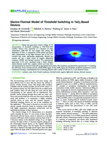
Research Articlewww.acsami.orgElectro-Thermal Model of Threshold Switching in TaOx‑BasedDevicesJonathan M. Goodwill,*,† Abhishek A. Sharma,‡ Dasheng Li,† James A. Bain,‡and Marek Skowronski*,††Department of Materials Science and Engineering, Carnegie Mellon University, Pittsburgh, Pennsylvania 15213, United StatesDepartment of Electrical and Computer Engineering, Carnegie Mellon University, Pittsburgh, Pennsylvania 15213, United States‡S Supporting Information*ABSTRACT: Pulsed and quasi-static current voltage (I V)characteristics of threshold switching in TiN/TaOx/TiNcrossbar devices were measured as a function of stagetemperature (200 495 K) and oxygen flow during thedeposition of TaOx. A comparison of the pulsed and quasistatic characteristics in the high resistance part of the I Vrevealed that Joule self-heating significantly affected thecurrent and was a likely source of negative differentialresistance (NDR) and thermal runaway. The experimentalquasi-static I V’s were simulated using a finite elementelectro-thermal model that coupled current and heat flowand incorporated an external circuit with an appropriate load resistor. The simulation reproduced the experimental I V includingthe OFF-state at low currents and the volatile NDR region. In the NDR region, the simulation predicted spontaneous currentconstriction forming a small-diameter hot conducting filament with a radius of 250 nm in a 6 μm diameter device.KEYWORDS: tantalum oxide, Poole Frenkel conduction, threshold switch, negative differential resistance, thermal runaway1. INTRODUCTIONThe ever-increasing need for faster and more energy- andspace-efficient ways to store data has driven the interest inpassive crossbar memory arrays. This design offers excellentscalability with the smallest possible cell size of 4F2, where F isthe minimum feature size, but suffers from the so-called sneakpath problem where all cells along the word and bit linescorresponding to the selected cell are half-selected. Theparasitic current flowing through these cells can cause readerrors and severely limits the array size. One way to reduce thesneak path problem is to incorporate a highly nonlinearselection device in series with the memory element.1 3Threshold switching devices are one of the candidates forthis application.4,5 This report is focused on one class of suchdevices, namely, structures based on transition metal oxideswith highly temperature dependent conductivity, and theunderlying mechanism of their operation.The current voltage (I V) characteristics of a thresholdswitch resemble the letter “S” and consist of three branches.The branch with the lowest current is referred to as the highresistance OFF-state, which continues until the slope of the I V becomes infinite at the threshold voltage (VTH). At highercurrents, the slope of the I V becomes negative, giving rise tothe intermediate branch known as the negative differentialresistance (NDR) region. The last region, the low resistanceON-state, is defined as the high-current region above the NDRregion where the slope of the I V becomes positive once again. 2017 American Chemical SocietyWhile the conductivity in OFF- and ON-states is thought to bemostly uniform, the NDR region exhibits formation of highcurrent density filaments.6 A number of mechanisms have beensuggested to give rise to NDR in different materials/devices.For example, in amorphous chalcogenides, the proposedmechanisms include double injection,7 field-induced filling oftraps,8 energy gain by electrons hopping between defect sites,9electric field-induced secondary phase nucleation,10 and eventhermal runaway,11,12 among others. In addition to amorphouschalcogenides, threshold switching has been extensively studiedin VO2 and NbO2 where it was generally interpreted as due to afield- or Joule heating-induced insulator-to-metal transition.13 18 There are only a few reports of threshold switchingin dielectric oxides such as TiOx, TaOx, or HfOx, and themechanism behind this phenomenon is not well established.19 21Three recent reports on NbOx offer some insight into theproposed mechanism of threshold switching in dielectricoxides, namely, thermal runaway.22 24 The three publicationsreport the quasi-static I V’s of NbOx-based devices and fit thedata with a Poole Frenkel-type formula to obtain conductivityas a function of temperature and electric field. Simulationsincluding self-heating showed that, at a certain voltage, theReceived: December 23, 2016Accepted: March 15, 2017Published: March 15, 201711704DOI: 10.1021/acsami.6b16559ACS Appl. Mater. Interfaces 2017, 9, 11704 11710
Research ArticleACS Applied Materials & InterfacesFigure 1. (a) Quasi-static I V measured at 300 K for a device with a 7.5% O2 flow TaOx film. The inset shows the low voltage characteristics. (b)Low field conductivities of devices fabricated with three different flow rates of oxygen during sputtering. (c) A comparison between the pulsed I V(triangles) and quasi-static I V (continuous lines) at different stage temperatures for a 7.5% oxygen film and (d) pulsed I V for the same film(triangles) versus the fit of the Poole Frenkel formula (lines) at different stage temperatures.fraction is not the same as the percentage of oxygen in the TaOx layer,nor are these two proportional. The devices fabricated with these filmswill be referred to by the respective O2 percentages of the ambient inwhich they were sputtered. The lateral size of the devices was 5 5μm, and they were patterned in a ground-signal-ground configurationallowing for short pulse measurements. The quasi-static I V’s wereobtained using a circuit consisting of the source and load resistor alongwith the device under test connected in series. The transient data wereobtained using Time Domain Transmissometry.27 The details of thefabrication, device layout, and experimental setups can be found in ourearlier publications.21,28 30 All data are plotted versus the voltageacross the device rather than source voltage.devices undergo thermal runaway. The estimated functionallayer temperature increase right before the threshold wasestimated to be 35 K24 and 150 K22 above the stagetemperature of 300 K. Both of these are far below theinsulator-to-metal transition in NbO2 at 1081 K.25,26 Thedevices discussed in these publications needed to be electroformed, a procedure that leads to the formation of a smalldiameter permanent filament consisting of a conductivereduced oxide. Neither the size nor the composition of thefilament is known. Moreover, the inhomogeneous material doesnot allow for observation and/or simulation of the salientfeature of a threshold switch, specifically, the spontaneouscurrent constriction in a structurally uniform device.In this work, we present experimental data on I Vcharacteristics of TiN/TaOx/TiN devices as a function ofstage temperature and deposition conditions of the TaOx film.These were simulated using a finite element modelincorporating coupled heat and current flow. The modelcorrectly describes the S-NDR characteristics and predicts thespontaneous current constriction to a small-diameter filamentof elevated current density and temperature. These insightsreveal some of the limitations of TaOx-based threshold switchesas selectors.3. RESULTSA typical experimental quasi-static I V of a tantalum oxidedevice structure is shown in Figure 1a. These data wereobtained at a stage temperature of 300 K on a 7.5% oxygendevice with a series load resistor of 26.7 kΩ. The devices werenot electroformed, and the current and dissipated power wereintentionally limited to 1 mA and 3 mW to prevent permanentchanges to the device. The initial characteristics remainedunchanged throughout the entire series of experiments, whichwas confirmed by measuring the high resistance statecharacteristics before and after the transition to the NDRregion. The I V shows the OFF-state at low voltages/currentswith gradually increasing slope until eventually becomingvertical at 10 V. The functional I(V) dependence in the OFFstate is discussed in detail below. At higher current, the slope ofthe I V becomes negative as the device enters the NDR region.Between 9.5 and 3.5 V, the I V shows a straight linecorresponding to a transition between two points in the NDRregion along the load line. Above the transition, the devicecurrent increases rapidly with small changes in voltage. Theinset in Figure 1a shows the I V at low voltages where theinitial current dependence is linear. This slope was used todetermine the low field conductivity for the simulationsdiscussed in the section below.The slope of the linear part of the I V as a function of thestage temperature and oxygen fraction is shown in Figure 1b.2. MATERIALS AND METHODSDevices with a TiN/TaOx/TiN structure were fabricated on a siliconwafer with 1 μm of thermal oxide. The metal insulator metalstructure consisted of 30 nm thick sputtered TiN electrodes and 150nm of functional reactively sputtered TaOx layer. Since the functionallayer was deposited on a nonplanar surface with a patterned bottomelectrode, the relative variations in film thickness over the edges of theelectrode are expected to be large. In order to minimize the effect ofsuch variations, a relatively large thickness of the functional layer waschosen. The TiN electrodes were sputtered at room temperature withan argon flow rate of 60 sccm and a chamber pressure of 3 mTorr. TheTaOx films were sputtered at room temperature with a chamberpressure of 3 mTorr, an oxygen flow of 3, 4.5, and 6 sccm, and aconstant total flow of Ar and O2 at 60 sccm. This corresponds to 5,7.5, and 10% of oxygen fraction in the sputtering ambient. This11705DOI: 10.1021/acsami.6b16559ACS Appl. Mater. Interfaces 2017, 9, 11704 11710
Research ArticleACS Applied Materials & InterfacesThe three functional layers spanned a conductivity range ofover 2 orders of magnitude at room temperature. Theconductivity of each device shows thermally activated behaviorwith activation energies ranging from 0.26 0.01 eV at lowoxygen content to 0.44 0.005 eV at high oxygen content.This suggests that the Fermi level in TaOx layers, which islocated close to the middle of the band gap in a stoichiometricmaterial, moves closer to the conduction band with decreasingoxygen content. The change is likely due to creation of trapsassociated with oxygen deficiency. The presence of traps inTaOx with energies of 0.2, 0.3, and 0.6 eV below theconduction band edge has been reported in thermallystimulated current measurements.31 Similar energies of trapshave been extracted from fitting the leakage current in TaOxbased structures with the Poole Frenkel formula.32,33The effect of Joule self-heating on the I V characteristics of atypical device can be assessed based on data shown in Figure1c. All data in this figure have been obtained on the same 7.5%O2 device at three different stage temperatures. The continuouslines represent experimental quasi-static voltage sweeps at aramp rate of 0.4 V/s, while the triangles denote pulsed I Vcharacteristics. The dwell time for each voltage step was ordersof magnitude longer than the device thermal time constant τo(estimated in our earlier publication to be 3 μs),28 and thedevice was able to reach a steady state temperature at everypoint on the curve. In contrast, the pulsed I V’s were measuredwith 30 ns long rectangular pulses with the readings taken at 10ns. A single pulse was applied every few seconds. The RC timeconstant determined by the device capacitance and itsresistance was about 3 ns, much shorter than the length ofthe pulse. The short pulse length Δt τo ensured the devicedid not heat up during the pulse as attested by current andvoltage remaining constant during the pulse for most datapoints. Only at large applied voltages did the current increaseslightly with a temperature rise calculated to be less than 10 K.As seen in Figure 1c, the quasi-static curves follow the pulsedones at low voltages but then increase faster with voltage. Thedivergence is due to Joule heating and the conductivityincreasing with temperature. Additionally, by overlaying pulsedI V characteristics obtained at different stage temperaturesonto a single quasi-static I V curve, it is possible to estimatethe increase of device temperature; the method was outlined byGala et al.34 As an example, the quasi-static I V curve at thestage temperature of 400 K diverges from the pulsed I V atapproximately 2.5 V. By the end of the quasi-static curve at 4 V,the current coincides with that obtained in a pulsed I Vcorresponding to a stage temperature of 435 K (not shown).Thus, we can infer that the device temperature increased by 35K due to Joule heating before the device reached VTH. It is alsoapparent that, even in the absence of Joule heating, the currentincreases superlinearly with voltage.The I(V) dependence of metal/TaOx/metal structures istypically interpreted as due to either a Schottky effect in thininterfacial barriers,35,36 field-enhanced emission from traps(Poole Frenkel model),23,37 40 or polaronic conductivity.24,41Most of the work to date indicates the Poole Frenkel model asbest describing the observations. We adopt this model here,taking the functional dependence of conductivity on field andtemperature as23,42σPF(F ,T ) σo(T )2 2 β F β F σo(T ) kBT 1 exp 1 F β kBT kBT (1)where Nd 2 Ed Et σo(T ) qμNc exp 2kBT Nt q3 1/2 β πεoεi (2)and constants Nd, Ed and Nt, Et correspond to the densities andionization energies of donors and traps, respectively, Nc is theeffective density of states in the conduction band, σo(T) is thelow field conductivity, μ is the electron mobility, kB is theBoltzmann constant, q is the elementary charge, εo is thepermittivity of free space, εi is the relative dielectric constant ofthe material, F is the electric field, and T is the stagetemperature. The σo(T) in the formula was determined fromthe experimental data in Figure 1b (energies (Ed Et)/2 ineach sample are equal to the activation energies). An additionalparameter, the dielectric constant, was used as an adjustableparameter, and the best fit was obtained for its value of 22. Thiscorresponds to the value of the low frequency constant, inagreement with other reports.32,33,43,44 It should be noted,however, that many publications argue for use of the highfrequency constant.35,38,39,45 The experimental data and fittingresults are shown in Figure 1d for the 7.5% O2 TaOx film atthree different stage temperatures. The fits are in goodagreement with experiment for all three types of functionallayers (not shown), stage temperatures, and fields.The finite element simulation assumed a 6 μm diametercylindrical device as part of the circuit consisting of the voltagesource and load resistor with the coupled current and heat flow.For electrical conductivity, we have used σPF(F,T) obtainedfrom fitting pulsed I V’s and extrapolated the experimentaldata range to higher temperatures as needed. The details of thesimulation are given in the Supporting Information. Theprocedure generated I V curves that reproduce the experimental quasi-static I V, including the superlinear behavior inthe OFF-state and the NDR region. The results are plotted inFigure 2 for three different stage temperatures and the deviceswith the functional layer deposited with 7.5% O2. The blue, red,and green lines represent the experimental data, while the blackdotted lines correspond to the simulation. The same data areplotted in the inset on a logarithmic scale to show the I V’s atlow current values. The simulation reproduced the exper-Figure 2. Experimental I V characteristics of TaOx based devices witha film deposited with 7.5% O2 in the chamber (thick color lines) andfinite element simulation of the same device (dotted lines) as afunction of voltage and stage temperature.11706DOI: 10.1021/acsami.6b16559ACS Appl. Mater. Interfaces 2017, 9, 11704 11710
Research ArticleACS Applied Materials & Interfacesresistance to 0.5 K/μW. Also worth noticing is that the currentdensity at the lateral edge is an order of magnitude lowercompared to the current density at the same location at VTH.This drop is due to the lower voltage across the device at point“2” than at VTH (as apparent in Figure 2). The temperature atthe center of the filament at this point is 1200 K. With a furtherincrease of total current, the calculated temperature isincreasing linearly with current with the fwhm increasing onlyslightly. The simulation is not reliable much beyond point “2”.The temperature is over 700 K past the highest stagetemperature used in the calibration shown in Figure 1, andthe Poole Frenkel formula likely deviates from the real valuesof electrical conductivity. Also, the thermal properties, whichare assumed independent of temperature, could have changedsignificantly.At this point, we would like to stress that the observedcurrent constriction to form the conducting filament is purelycaused by local Joule heating of the functional layer. The devicecharacteristics have not changed as the result of testing,indicating that no physical changes occurred in the structure. Ifchanges such as crystallization of the initially amorphousmaterial have occurred,46 they have not affected the electricalcharacteristics. This is different than in similar memory-typecells which undergo ion redistribution.47,48 Permanent physicalchanges do occur in these structures at current densities andtime-at-voltage just slightly above those used in this work.These were intentionally avoided during testing.imental data quite well: the curve in the OFF-state at alltemperatures overlaps with and/or is parallel to theexperimental curve, the threshold voltage is within 5% of theexperimental value, and the NDR regions coincide. Similaragreement was obtained for devices with different oxygen flowrates.More insight into the characteristics of threshold switchingcan be obtained from evolution of temperature and currentdensity with voltage. The 3-D temperature distribution mapsfor the two points marked “1” and “2” in Figure 2 for a devicewith a 7.5% O2 layer at a stage temperature of 300 K are shownin Figure 3a. Figure 3b shows the corresponding line profiles of4. DISCUSSIONFor all biasing conditions and stage temperatures, the electricalconductivity of the functional layer is much lower than theconductivity of the metallic electrodes, resulting in a laterallyuniform voltage across the electrodes. This results in a uniformcurrent flow and uniform heating at low dissipated power.Upon approaching VTH, the temperature in the center of thedevice increases and the functional layer becomes a littlewarmer and more conductive than the lateral boundaries of thedevice. The current and temperature form a positive feedbackloop where increases in current cause increases in temperature,and this, in turn, increases current further. The conditions forthe runaway can be estimated in a simple model in which theelectrical resistivity as a function of temperature is approximated by the linear term in the Taylor seriesFigure 3. (a) Temperature and (b) current density distribution in the7.5% O2 device corresponding to points “1” (at VTH, continuous blueline) and “2” (within NDR region, dotted red line) in Figure 2.current density along the radius of the device. Point “1”corresponds to the knee of current at VTH. The averagetemperature of the functional layer increased by about 50 Kabove the stage temperature of 300 K with the center of thedevice being 30 K higher than the lateral edges. Thecorresponding current density ratio is a factor of 2. Thevariations across the device at this point are due to lateral heatflow. At point “2” in the NDR region, the current density andtemperature distribution are highly nonuniform even thoughthe voltage across the device is the same everywhere. Thecurrent density in the center of the device is about 4 orders ofmagnitude higher than the current density at the lateral edgewith the full width at half-maximum (fwhm) of 250 nm. It isinteresting to note that the thermal resistances of the OFF-stateand NDR regions are different from each other. In the OFFstate, the current and power dissipation is more or less uniformacross the diameter of the device, corresponding to a thermalresistance of 0.05 K/μW. In the NDR region, power dissipationis confined to a much smaller area, increasing the thermal 1 σV IRo 1 IVRTH ··· σ(To) T (3)where Ro is the resistance at the stage temperature, σ is theelectrical conductivity, and RTH is the thermal resistancebetween the functional layer and the heat sink. The runawaywill occur when V/ I is zero, leading toIV σ(To) σ 1 2RTH T (4)This gives the value of resistance at runaway R(T) Ro/2.Thus, runaway will occur when the Joule heating causes theresistance to drop by a factor of 2 and can occur at verydifferent temperatures of the filament depending on the stagetemperature. It is easy to notice that the quasi-static current atvoltages approaching VTH is, in fact, about twice that of thecurrent in the pulsed I V’s (Figure 1c).11707DOI: 10.1021/acsami.6b16559ACS Appl. Mater. Interfaces 2017, 9, 11704 11710
Research ArticleACS Applied Materials & Interfacesand load resistor, and heat and current flow. The currentdensity as a function of electric field and temperature wasobtained from short pulse I V measurements. It was shownthat the threshold switching in TaOx could be well accountedfor by a thermal runaway process leading to the formation of asmall-diameter hot filament. The thermal runaway is shown tobe a direct consequence of the strong dependence ofconductivity on temperature.There are two possible scenarios for the end of a runaway. Ifthe circuit includes a small load resistor, the voltage across thedevice will remain approximately constant during the runaway.The filament will expand and its temperature will keepincreasing until the device is destroyed. On the other hand, ifthe load resistance is significantly larger than the resistance ofthe filament, the voltage drop across the device will decrease,limiting the total dissipated power. The device will come to thesteady state with a small-diameter hot filament.Figure 4a compares the experimental and simulated values ofthe threshold voltage for three different functional layers as a ASSOCIATED CONTENTS Supporting Information*The Supporting Information is available free of charge on theACS Publications website at DOI: 10.1021/acsami.6b16559.Device structure and material parameters and justification used in COMSOL simulation of experimental I Vcurves (PDF) AUTHOR INFORMATIONCorresponding Authors*E-mail: jgoodwil@andrew.cmu.edu (J.M.G.).*E-mail: Mareks@cmu.edu (M.S.).ORCIDJonathan M. Goodwill: 0000-0002-3466-3350Marek Skowronski: 0000-0002-2087-0068Author ContributionsThe manuscript was written through contributions of allauthors. All authors have given approval to the final version ofthe manuscript.NotesThe authors declare no competing financial interest. Figure 4. Comparison between the experimentally measured (solidlines) and simulated (dashed lines) threshold voltage (a) andthreshold power (b) for devices with three different O2 flows.ACKNOWLEDGMENTSThis work was supported in part by FAME, one of six centersof STARnet, a Semiconductor Research Corporation programsponsored by MARCO and DARPA and by NSF Grant DMR1409068.function of stage temperature. There are two apparent trends:VTH is decreasing with increasing oxygen deficiency and stagetemperature. It should be kept in mind that the conductivitiesof all devices are increasing with stage temperature and thecurrent at VTH is increasing even though VTH is decreasing. Thepower at the beginning of the runaway (Figure 4b) is increasingwith the stage temperature for both experiment and simulation.The decrease of VTH at lower O2 content in the ambient isassociated with the decreasing activation energy of theconductivity. It results in a lower σ/ T, which means that agreater change of temperature is necessary to halve the initialresistance and, hence, higher dissipated power is required forthe runaway. At low stage temperatures and oxygendeficiencies, the only way to increase dissipated power is toincrease the VTH. A similar decrease of VTH with an increase ofstage temperature was reported in our earlier work on TaOx34and other oxides.22,23,49 Lastly, it is important to notice that thepredicted size of the hot filament, while small, is much biggerthan the size of the access devices to be used in memory arrays.The 10 nm-size devices retain the general shape of their I Vcharacteristics (simulated), i.e., exhibit NDR and thresholdswitching. The scaling behavior is somewhat complex and willbe described in a separate publication. REFERENCES(1) Zhou, J.; Kim, K.-H.; Lu, W. Crossbar RRAM Arrays: SelectorDevice Requirements During Read Operation. IEEE Trans. ElectronDevices 2014, 61 (5), 1369 1376.(2) Zhang, L.; Cosemans, S.; Wouters, D. J.; Groeseneken, G.;Jurczak, M.; Govoreanu, B. Selector Design Considerations andRequirements for 1S1R RRAM Crossbar Array. In IEEE 6thInternational Memory Workshop; IEEE Computer Society, 2014.(3) Kim, S.; Zhou, J.; Lu, W. D. Crossbar RRAM Arrays: SelectorDevice Requirements During Write Operation. IEEE Trans. ElectronDevices 2014, 61 (8), 2820 2826.(4) Jo, S. H.; Kumar, T.; Narayanan, S.; Lu, W. D.; Nazarian, H. 3DStackable Crossbar Resistive Memory Based on Field AssistedSuperlinear Threshold (FAST) Selector. In IEEE International ElectronDevices Meeting; IEEE, 2014.(5) Song, J.; Woo, J.; Prakash, A.; Lee, D.; Hwang, H. ThresholdSelector With High Selectivity and Steep Slope for Cross-PointMemory Array. IEEE Electron Device Lett. 2015, 36 (7), 681 683.(6) Ridley, B. K. Specific Negative Resistance in Solids. Proc. Phys.Soc., London 1963, 82 (6), 954 966.(7) Adler, D.; Henisch, H. K.; Mott, N. The Mechanism of ThresholdSwitching in Amorphous Alloys. Rev. Mod. Phys. 1978, 50 (2), 209 220.(8) Adler, D.; Shur, M. S.; Silver, M.; Ovshinsky, S. R. ThresholdSwitching in Chalcogenide-Glass Thin Films. J. Appl. Phys. 1980, 51(6), 3289 3309.5. CONCLUSIONSThe quasi-static I V characteristics of different compositions ofTaOx were experimentally measured and simulated by a finiteelement model that included power distribution between device11708DOI: 10.1021/acsami.6b16559ACS Appl. Mater. Interfaces 2017, 9, 11704 11710
Research ArticleACS Applied Materials & InterfacesProcess in TiO2 Based Resistive Switching Devices. Appl. Phys. Lett.2013, 102 (2), 023507.(29) Noman, M.; Sharma, A. A.; Lu, Y. M.; Kamaladasa, R.;Skowronski, M.; Salvador, P. A.; Bain, J. A. Mechanism of LocalizedElectrical Conduction at the Onset of Electroforming in TiO2 BasedResistive Switching Devices. Appl. Phys. Lett. 2014, 104 (11), 113510.(30) Sharma, A. A.; Noman, M.; Skowronski, M.; Bain, J. A. HighSpeed In-Situ Pulsed Thermometry in Oxide RRAMs. In Proceedings ofthe Technical Program - International Symposium on VLSI Technology,Systems and Application (VLSI-TSA); IEEE, 2014.(31) Lau, W. S.; Tan, T. S.; Sandler, N. P.; Page, B. S.Characterization of Defect States Responsible for Leakage Currentin Tantalum Pentoxide Films for Very-High-Density DynamicRandom Access Memory (DRAM) Applications. Jpn. J. Appl. Phys.1995, 34 (Pt. 1, No. 2B), 757 761.(32) Wu, X. M.; Soss, S. R.; Rymaszewski, E. J.; Lu, T.-M. DielectricConstant Dependence of Poole-Frenkel Potential in Tantalum OxideThin Films. Mater. Chem. Phys. 1994, 38 (3), 297 300.(33) Ezhilvalavan, S.; Tseng, T.-Y. Conduction Mechanisms inAmorphous and Crystalline Ta2O5 Thin Films. J. Appl. Phys. 1998, 83(9), 4797 4801.(34) Gala, D. K.; Sharma, A. A.; Li, D.; Goodwill, J. M.; Bain, J. A.;Skowronski, M. Low Temperature Electroformation of TaOx-BasedResistive Switching Devices. APL Mater. 2016, 4 (1), 016101.(35) Blonkowski, S.; Regache, M.; Halimaoui, A. Investigation andModeling of the Electrical Properties of Metal-Oxide-Metal StructuresFormed from Chemical Vapor Deposited Ta2O5 Films. J. Appl. Phys.2001, 90 (3), 1501 1508.(36) Zeng, W.; Eisenbraun, E.; Frisch, H.; Sullivan, J. J.; Kaloyeros, A.E.; Margalit, J.; Beck, K. CVD of Tantalum Oxide Dielectric ThinFilms for Nanoscale Device Applications. J. Electrochem. Soc. 2004, 151(8), F172 F177.(37) Young, P. L. DC Electrical Conduction in Thin Ta2O5 Films. I.Bulk-Limited Conduction. J. Appl. Phys. 1976, 47 (1), 235 241.(38) Oehrlein, G. S. Oxidation Temperature Dependence of the DcElectrical Conduction Characteristics and Dielectric Strength of ThinTa2O5 Films on Silicon. J. Appl. Phys. 1986, 59 (5), 1587 1595.(39) Choi, W. K.; Ling, C. H. Analysis of the Variation in the FieldDependent Behavior of Thermally Oxidized Tantalum Oxide Films. J.Appl. Phys. 1994, 75 (8), 3987 3990.(40) Spassov, D.; Atanassova, E.; Virovska, D. Electrical Characteristics of Ta2O5 Based Capacitors with Different Gate Electrodes. Appl.Phys. A: Mater. Sci. Process. 2006, 82 (1), 55 62.(41) Bryksin, V. V.; Goltsev, A. V.; Khanin, S. D.; Novotelnova, A. V.;Vasilev, A. N. Nonlinear Current-Voltage Characteristics of Ta2O5 andNb2O5 Amorphous Oxides. Phys. Status Solidi B 1990, 161 (2), 777 781.(42) Hartke, J. L. The Three-Dimensional Poole-Frenkel Effect. J.Appl. Phys. 1968, 39 (10), 4871 4873.(43) Hughes, D. M.; Jones, M. W. Electrical Conduction inReactively Sputtered Tantalum Oxide Thin Films. J. Phys. D: Appl.Phys. 1974, 7, 2081 2096.(44) Chiu, F.; Wang, J.; Lee, J. Y.; Wu, S. C. Leakage Currents inAmorphous Ta2O5 Thin Films. J. Appl. Phys. 1997, 81 (10), 6911 6915.(45) Oehrlein, G. S.; Reisman, A. Electrical Properties of AmorphousTantalum Pentoxide Thin Films on Silicon. J. Appl. Phys. 1983, 54(11), 6502 6508.(46) Kwon, J.; Sharma, A. A.; Chen, C. Y.; Fantini, A.; Jurczak, M.;Herzing, A. A.; Bain, J. A.; Picard, Y. N.; Skowronski, M. TransientThermometry and High-Resolution Transmission Electron Microscopy Analysis of Filamentary Resistive Switches. ACS Appl. Mater.Interfaces 2016, 8 (31), 20176 20184.(47) Wong, H.-S. P.; Lee, H.-Y.; Yu, S.
Electro-Thermal Model of Threshold Switching in TaO x‑Based Devices Jonathan M. Goodwill,*,† Abhishek A. Sharma,‡ Dasheng Li,† James A. Bain,‡ and Marek Skowronski*,† †Department of Materials Science and Engineering, Carnegie Mellon University, Pittsburgh, Pennsylvania 15213, United States ‡Department of Electrical and Computer Engineering, Carnegie Mellon University .