Transcription
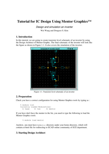
Tutorial for IC Design Using Mentor Graphics Design and simulation an inverterWei Wang and Dongsoo S. Kim1. IntroductionIn this tutorial, we are going to create transistor level schematic of an inverter by usingthe Design Architect of Mentor Graphic. The final schematic of the inverter will look likethe figure as shown in Figure 1-1. It also covers the simulation of the inverter.Figure 1-1. Transistor level schematic of an inverter2. PreparationCheck you have a correct configuration for using Mentor Graphics tools by typing as :% module listCurrently Loaded Modulefiles:1) base2) tex3) mentorIf you have don't have the mentor in the list, you need to type the following to load theMentor Graphics tools:% module load mentorAnyhow, you must have MyMentor directory under your home directory, which willcontain a n html file for redirecting to ECAD online community of ECE department.3. Starting Design Architect
1. Invoke Design Manager by typing: adk daic &The Design Manager window will appear as shown in Figure 3-1.Figure 3-1. The Design Manager window3. Double click da ic icon in the 'Tools' window and wait for a couple ofseconds, the Design Architect window will appear. Select Schematic inthe Session Palette window. A dialog box pops up as shown in Figure 32.Figure 3-2 Dialog box for open new sheet4. In the box labeled Component Name , type the schematic name inverterat the end of default path. If you want to indicate the another directory, usethe Navigator, select the directory name, and type inverter at the end.5. Leave other boxes untouched and click OK. For an existing design, you
may use the navigator to locate the component in your directories.4. Schematic Entry4.1 Adding components and ports to the schematicSelect the parts for your schematic of the inverter by choosing from a libraryof components.1. In the schematic edit palette, select Library. Click on Device Lib toplace the transistors - an NMOS(4-pin) and a PMOS(4-pin).2. Click on Generic Lib to place Portin, Portout, VDD, and Ground asshown in Figure 4-1.Figure 4-1 The required components in schematic diagram4.2 Add Text/Change Labels To add text on the sheet:1. Click Text on the right side palette, then select Comment Text.2. Enter the text in the prompt bar, then click on OK.3. Move cursor and click to place the text on the sheet. To change the text or name of the ports:1. Place the cursor on the port name. Press Shift key and F7 simultaneously.2. A Display Prompt Bar appears in the bottom of the the schematicwindow. Input the new name in the New Value box, then click OK asshown in Figure 4-2.
Figure 4-2. The port name.4.3 WiringIn the schematic edit palette, select WIRE (or press F3). For adding a wire betweentwo points click once at the starting point and at all intermediate points to define thenet route and double click at the end point to complete the routing.Figure 4-3. Add wires.4.4 Change the instance name of the componentsTo change the reference number (INST), select the component, click right mouse button,and then select Properties Modify Multiple. In the box of Instance, change theASIM MODEL, INST, L, and W values as shown in Figure 4-4.To change the reference number automatically highlight all components, click the rightmouse button, Instance Alter. The reference numbers will be automatically generatedby the tool.
Fig 4-4. Change the properties5. Check/Save the sheet1. The schematic you have created needs to be checked for connection errors beforeit is saved into a file. Press Check& Save from the schematic edit palette tocheck and save your sheet. If your sheet does not pass the check, you cannot getthe result of simulation of the design. Check the log if errors are listed.2. To prepare a Viewpoint for simulation in DA IC, click Simulation in the palette,click OK, and then click EndSim. (To make sure the Netlist is SPICE Netlisterand Viewpoint name is eldonet by click option as shown in Figure 5-1.)
Figure 5-1. Setup Default Viewpoint6. Generate Symbol1. After your schematic is completed, you may want to create a block symbol torepresent this circuit. This symbol can be used in other schematics to perform thesame function as this circuit, and you do not need to draw the same circuit again.2. Make sure that the schematic is checked and saved before making the symbol. Togenerate a symbol, select:M iscellaneous - Generate Symbol.from the pull-down menu bar.3. In General Symbol dialog box, select Choose Shape , and select Buffer, clickOK , and click OK. A Symbol is created automatically and is displayed in a newwindow as shown in Figure 6-1.Fig 6-1. The symbol of Inverter.
4. Edit symbol if necessary. Use the same skill as in editing the schematic.5. To save the symbol, press Check& Save from the schematic edit palette tocheck and save your sheet.7. Simulation7.1 Create a test circuit1. Close your inverter and symbol, open a new sheet, and name it test inverter.2. Add one instantiation of inverter cell by selectingAdd - Instrance - Choose SymbolChoose Inverter and click OK, we will get the symbol of the inverter as shown inFigure 7-1.Figure 7-1. One instantiation of an inverter3. Add DC source at the input of inverter, add Portout at the output, createpower supply for the circuit, and change the value of DC source and Pulsesource from 1 V to 3.3 V.4. Check & Save7.2 Set up the model1. Click Simulation in the schematic edit palette to invoke the simulation, andclick OK.2. Include TSMC0.35 m BSIM3 model, click Library in schematic sim palette,and type ‘ ADK/technology/accusim/tsmc035.mod’ in Library path and thenclick OK.7.3 DC AnalysisYou will run a DC sweep of the input and view the results.1. Cliick Analysis in Setup Sim header inside schematic sim palette, select D Cand click Setup.In the setup box that appears, type ‘IN’ for ‘Voltage Source’, ’0’ for 'Start' boxand '3.3' for 'Stop' field, click OK, and then click OK as shown in Figure 7-2.
Figure 7-2. Setup Voltage Source2. To view the input and output of your inverter, highlight IN and OUT,click Setup Results Plots. Select DC, select Voltage, and then click OKClick Setup Results Probes. Check DC, select Voltage, and then click OK3. To run the simulation, click Netlist Write and Simulation- Run.4. To view the results of your dc sweep, click Results View Invoke Viewe r. ClickResult Xprobe Voltages-Default.5. Drag cover input port and output port.6. Press the right mouse bottom and from the popup menu select Chart Addcursor.Then type Cursor name: T0 OKPress the left mouse button on the cursor and drag the cursor to the voltage pointyou wantto measure.To obtain another cursor to measure between points, press the right mouse bottomand fromthe popup menu select Chart Add cursor. Then type Curs or name: T1 OKPress the left mouse button on the cursor and drag the cursor to the second voltagepoint youwant to measure.7. Another method to view the results of the analysis is by listing the signal values.Select Vin Vout and the right mouse botto m, and select LIST . A LIST windowwill appearwith a list of values for Vin and Vout.8. Print your waveform by selecting the trace window, and selecting File PrintChart with ICPrint from the menu. Type laser for the printer name.7.4 Transient AnalysisIn this section, you will provide a pulse at the input and view the results.1. Instead of using DC Source by using Pulse Source, connect to the input ofinverter as shown in Figure 7-3.
Figure 7-3. The schematic for Transient Analysis2. Click Setup Sim - Analysis, select Transient, click Setup. In the setup box thatappears, type 10u for Stop Time field and 50n for Time Step box. Then click onOK.3. To view the input and output of your inverter, highlight IN and OUT, and clickSetup Results Plots. Check TRAN, select Voltage, and then click OK.Click Setup Results Probes. Check TRAN, select Voltage, and then click OK4. To run the simulation, click Netlist Write and Simulation- Run.5. View the results by clicking Results View Invoke Viewe r. Click Result Xprobe Voltages-Defaultas shown in Figure 7-4.6. You can probe, measure and view your results as in the previous section.Figure 7-4. The results of Transient Analysis7.5 DC Operating point AnalysisIn this section, you will find the DC operating point of several nodes in the circuitand look at the transfer function of the input.1. Setting up the simulationClick Setup Sim - Analysis.Select DCOP in the dialog box that appears,then click OK2. Running the simulationClick Netlist Write and Simulation- Run.3. Viewing the results
The next step is to view the results of your simulation run.To see all the DC voltages and currents in your schematic,Click DCOP Show Both
1. Invoke Design Manager by typing: adk_daic & The Design Manager window will appear as shown in Figure 3-1. Figure 3-1. The Design Manager window 3. Double click da_ic icon in the 'Tools' window and wait for a couple of seconds, the Design Architect window will appear.Select Schematic in the Session Palette window.A dialog box pops up as shown in Figure 3-