Transcription
sensorsArticleOptical Planar Waveguide Sensor with IntegratedDigitally-Printed Light Coupling-in andReadout ElementsJorge Alamán 1,2 , María López-Valdeolivas 1 , Raquel Alicante 1 andCarlos Sánchez-Somolinos 1,3, *123*Instituto de Ciencia de Materiales de Aragón (ICMA), CSIC-Universidad de Zaragoza, Departamento deFísica de la Materia Condensada, 50009 Zaragoza, SpainBSH Electrodomésticos España, S.A., Polígono Industrial de PLA-ZA, Ronda del Canal Imperial de Aragón,50197 Zaragoza, SpainCentro de Investigación Biomédica en Red de Bioingeniería, Biomateriales y Nanomedicina (CIBER-BBN),C Mariano Esquillor s.n., 50018 Zaragoza, SpainCorrespondence: carlos.s@csic.es; Tel.: 34-8765-53770Received: 17 May 2019; Accepted: 25 June 2019; Published: 27 June 2019 Abstract: Optical planar waveguide sensors, able to detect and process information from theenvironment in a fast, cost-effective, and remote fashion, are of great interest currently in differentapplication areas including security, metrology, automotive, aerospace, consumer electronics, energy,environment, or health. Integration of networks of these systems together with other optical elements,such as light sources, readout, or detection systems, in a planar waveguide geometry is greatlydemanded towards more compact, portable, and versatile sensing platforms. Herein, we reportan optical temperature sensor with a planar waveguide architecture integrating inkjet-printedluminescent light coupling-in and readout elements with matched emission and excitation. The firstluminescent element, when illuminated with light in its absorption band, emits light that is partiallycoupled into the propagation modes of the planar waveguide. Remote excitation of this elementcan be performed without the need for special alignment of the light source. A thermoresponsiveliquid crystal-based film regulates the amount of light coupled out from the planar waveguide at thesensing location. The second luminescent element partly absorbs the waveguided light that reachesits location and emits at longer wavelengths, serving as a temperature readout element throughluminescence intensity measurements. Overall, the ability of inkjet technology to digitally printluminescent elements demonstrates great potential for the integration and miniaturization of lightcoupling-in and readout elements in optical planar waveguide sensing platforms.Keywords: integrated optical planar waveguide sensors; flexible sensors; organic-inorganic hybridmaterials; liquid crystalline thermoresponsive materials; inkjet printing; luminescent materials1. IntroductionSensors are often described as platforms able to detect information, for example temperature,pressure, humidity, or the presence of chemical compounds, from the environment and transform thisinformation into different signals. Most common sensors usually respond to an external stimulus withan electrical signal that is later transmitted and processed by other electronic systems to which theyare interfaced. The language spoken between sensors and devices in these cases is therefore basedon the flux of electrons; however, the flux of photons can similarly be used to transfer informationin sensing platforms. Optical sensors present attractive features when compared with electricalones, since, for example, they are not subjected to electromagnetic interference, so they can be usedSensors 2019, 19, 2856; doi:10.3390/s19132856www.mdpi.com/journal/sensors
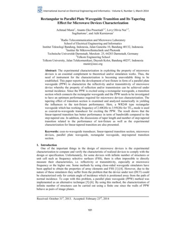
Sensors 2019, 19, 28562 of 14in a harsh environment with high voltages or intense magnetic fields. Besides, the possibility totransfer information through optical waveguides enables the generation of sensor networks that canbe connected and monitored remotely without the need to transform the detected information intoan electrical signal at each sensing site. The use of light with different properties (e.g., wavelength)also provides the possibility to multiplex several signals in a single waveguide easily. Even more, theemployed waveguides can be lightweight, flexible, and inexpensive. All these characteristics makeoptical sensing platforms of great interest in different application areas including metrology, qualityand process control, security, or (bio)medicine [1–5].An optical sensor typically entails different components such as photonic sources to generate theprobing light, optical elements to condition and direct this light towards the sensing region, as well asreadout devices to obtain the analysis results. In this field, optical fiber sensors have reached a highdegree of development. Coupling of light from lasers or light-emitting diodes (LEDs) is routinelyperformed currently by means of optical fiber couplers, and progress in sensing materials has enabledthe implementation of sensors with improved sensitivity, portability, and reduced size [6,7].Besides sensors relying on optical fibers, optical sensing systems integrated in planar waveguidegeometries have also been extensively explored as they can integrate networks of sensing elementsover large areas [8–10]. In these planar systems, it is highly desirable to miniaturize and integrateoptical elements of the sensing platform such as detection and readout systems or light sources inthe planar waveguide [11–14]. Moreover, for application areas such as biomedicine, microfluidics,or electronic skin, other specific requirements such as the compatibility with materials of differentnatures (e.g., glass, polymer, or metal), conformability, bendability, or stretchability need to beproperly addressed to contribute to the overall sensing device performance [15–18]. Besides, theuse of easily scalable, flexible, and reliable high-throughput fabrication techniques to synergisticallycombine photonic and sensing elements in thin films is required for the further development ofthese technologies. In this direction, a large effort is currently being made towards the developmentof materials and compatible manufacturing technologies enabling the large-scale, high-speed, andlow-cost production and preparation of microoptical elements, as well as planar photonic systems onpolymer foils. Waveguides have been generated in flexible substrates through, for example, laminationor inkjet-printing methods [19–25]. Interestingly, luminescent acrylate formulations have been appliedthrough inkjet printing on polymeric waveguides generated on poly(methyl methacrylate) (PMMA)substrates by Bollgruen and coworkers to create remotely-addressable light sources that can couplelight into flexible waveguides [26]. Moreover, regarding the sensing method, it is well known that theuse of luminescence intensity measurements to perform magnitude readout advantageously leads tosensitivity improvement when there is no overlap between the exciting and emitted light spectra [27].Even more, in a waveguide geometry, the light not absorbed in the readout element can be guided awayfrom the detection region, further facilitating discrimination of the luminescence from the excitationlight, leading to improved quality of the detectable signal.In this paper, we present an optical temperature sensor having a planar waveguide architectureand including two luminescent layers with matched emission properties. These two emissive elementsallow integrating light coupling-in and readout functions in the planar waveguide structure (Figure 1).Illumination of the first luminescent element with light in its absorption band induces emission of lightthat is partially coupled into the guided modes of the planar waveguide. Excitation of this element canbe remotely performed without the need for special alignment of the light source. As temperaturesensing materials, we include liquid crystalline polymers (LCP). The changes of molecular order in thesesystems, in response to temperature variations, make them suitable materials for this purpose [28–31].Changes in light scattering of the liquid crystalline (LC) polymeric film with temperature enable theregulation of the light coupled out from the waveguide at this location. Besides temperature sensing,used in this paper as a simple example, LC materials could be tailored to be responsive to other stimulisuch as moisture, pH, or chemical compounds as well [32–37]. After passing the region of the sensingelement, light remaining in the waveguide reaches the second luminescent element. The emission
Sensors 2019, 19, x3 of 13well [32–37]. After passing the region of the sensing element, light remaining in the waveguideSensors 2019, 19, 28563 of 14reaches the second luminescent element. The emission wavelength range of the first element ischosen to overlap with the excitation band of the second one, so the light generated in the firstwavelengthrangeof the firstelementintois chosento overlapserveswith theexcitation forbandthe secondone,element,whichis partiallycoupledthe waveguide,as excitationtheofsecondelementso thelightlightgeneratedin thefirst element,which is partiallyinto theoutwaveguide,servestheasthatemitsat longerwavelengths.Temperaturereadoutcoupledcan be carriedby measuringexcitation for thesecondofelementthat emitsat longer wavelengths.Temperaturereadoutcan beluminescenceintensitythis element.For lightthe implementationof the twoluminescentfunctionalcarried outmeasuringintensity of this element.the implementationof the twolayers,weby makeusetheofluminescenceour recently-developedinkjet Forprintingplatform 8]. organic-inorganicInkjet printing, hybridenablingthe digitaldepositionof materials,has [24,38].beenInkjet printing,toenablingthe digitalof materials,been demonstratedto bea powerfuldemonstratedbe a powerfultooldepositionfor the preparationandhasintegrationof functionalelementsandtool for mentsandtechnologydevices in aallowsflat geometry[25,39–46].devicesin apreparationflat geometrycase, inkjetprintingthe integrationinIn our case,inkjet printingtechnologythe integrationin planarwaveguidestructuresof lightplanarwaveguidestructuresof lightallowscoupling-inand readoutelements.Withthe presentedcoupling-in andreadoutelements.Withthe presentedphotonicelementssuch asfromlightarchitecture,photonicelementssuchas lightsources orarchitecture,detectors canbe physicallyseparatedsourcesor detectorscanallowingbe physicallyseparatedsensing device,still allowingremote andthesensingdevice, stillremoteand easyfromlightthecoupling-inand readout;and therefore,theeasyoflightcoupling-inand readout;and therefore,theexample,use of thesensor humidityin adverseorenvironmentswith,usethe sensorin adverseenvironmentswith, forextremehigh electricalorfor example,extremeor high electricalfields.Theandimplementationof the sensorsmagneticfields.Thehumidityimplementationof theor magneticsensors inrigidflexible waveguidesisalsodemonstrated.in rigidand flexible waveguides is also demonstrated.Figure 1.1. OpticalOptical planarplanar waveguidewaveguide sensorsensor withwith integratedintegrated digitally-printeddigitally-printed luminescentluminescent lightlightFigurecoupling-in andof ofthethefirstluminescentelement,by usingan LEDcoupling-inand tionexcitationfirstluminescentelement,by eguide.LightisguidedtowardsthethermoresponsiveLED for example, enables coupling of light into the waveguide. Light is guided towards theLCP element that regulatesthe lighttowards transmittedthe end of thewaveguidewherethethermoresponsiveLCP elementthatintensityregulatestransmittedthe light intensitytowardsthe endof ide where the second luminescent element is placed. (a) Scattering/non-transmissive state, atis scatteredout of thewaveguideat ivelowtemperature:lightis scatteredoutof the waveguideat smissive state, at high temperature: light is not scattered at the stimuli-responsivepropagatesandin thewaveguideandfurtherreaches propagatesthe second luminescentlayer. Remoteelement,therefore,lightin the waveguideand luminescencereaches the intensitysecondmeasurements allow quantifying the temperature in the sensor range.luminescent layer. Remote luminescence intensity measurements allow quantifying the temperaturein the sensor2. Materialsandrange.Methods2.Materialsand Methods2.1.Planar WaveguidesCleaningprocedure: Microscope glass slides (Thermo ScientificTM SuperFrost , extra-white2.1. PlanarWaveguidessoda-lime glass, dimensions: 76 mm 26 mm, 1 mm thick, n 1.517 at 546 nm) were employed asCleaningprocedure:Microscopeglass slides(Thermo ScientificTMextra-whiteplanarwaveguidesin someof the experiments.Pre-cleaningof these glassSuperFrost ,slides using soapywatersoda-limeglass,dimensions:76mm 26mm,1mmthick,n 1.517at546nm)wereemployedaswas carried out by gently rubbing the glass surface, using nitrile gloves. The slides were rinsed withplanarwaveguidesin somethe experiments.theseglassAfterslidesthis,usingwater andintroducedin an ofultrasonicbath withPre-cleaningsoapy wateroffor10 min.thesoapyglass e refluxed with Milli-Q water and ultrasonicated again in Milli-Q water for 10 min. The ywaterfor10min.Afterthis,theglassslideswere then flushed with isopropyl alcohol. A third ultrasonic bath was carried out, in this case withwererefluxedwithandtheultrasonicatedagainin withMilli-Qwater for air.10 min. The slidesisopropylalcoholforMilli-Q10 min.waterFinally,substrates weredriedcompressedwere Cyclicthen scarriedout,this atcaseolefin polymer (COP) foil from Zeonor (188 µm-thick polymer foil, n in1.53589withnm,isopropylalcoholfor 10 andmin. microscopeFinally, the substratesweredried withDusseldorf,Germany)COP slides,suppliedfromcompressedBeonCHIP air.(Zaragoza, Spain),olefinpolymer(COP) foil COPfrom rigidZeonor(188wereμm-thickpolymerfoil,n used1.53 asat received.589 nm,wereCyclicused BeonCHIP(Zaragoza,Spain),The flexible foil substrate was provided with a protective foil that was removed just before processing.
Sensors 2019, 19, 28564 of 142.2. Substrate TreatmentsUV ozone treatment was performed on a UV ozone reactor UVO 342 (Jelight company Inc., Irvine,CA, USA) to remove any contamination in the glass substrates, leaving silanol groups exposed on thesurface [38]. As a result, important changes in the wettability and in the adhesion were obtained [24].2.3. Surface Functionalization with FluorosilaneThe glass substrates, cleaned as described above, and UV ozone treated for 1 hour, were placed in adesiccator containing a glass slide with 50 µL of 1H,1H,2H,2H-perfluorooctyltrichlorosilane (PFOTClS)from Aldrich. A vacuum was applied in the desiccator until a pressure of 100 mbar was achieved.After 30 min, the substrates were taken out, thoroughly rinsed with isopropyl alcohol, dried withcompressed air, and heated for 10 min at 110 C in air [47].2.4. Temperature-Responsive Liquid Crystalline Material6-(4-Cyano-biphenyl-40 -yloxy)hexyl acrylate (A6OCB, also known as RM 105), a pro-mesogenicmolecule functionalized with one reactive acrylate group, was acquired from Synthon GmbH underthe reference STO3474. A6OCB presents a crystalline phase at room temperature (RT) and melts at70–71 C. ethylbenzene (RM82) from Merck isa mesogen functionalized with two acrylate end groups. 1-Hydroxycyclohexyl phenyl ketone, alsoknown as Irgacure 184 (IRG184), was used as a UV photoinitiator. A mixture comprising 99 wt% ofA6OCB and 1 wt% of RM82 was prepared as a precursor of the thermoresponsive LCP. Besides, 3 wt%of IRG184 photoinitiator was added. To help mixture homogenization, dichloromethane (CH2 Cl2 ) inan equivalent wt% to the weight of the solid material was added. The solids immediately dissolvedjust after a mild shaking of the containing flask. Afterwards, the flask remained open overnight in afume hood, and the weight was controlled the day after, confirming that all the dichloromethane hadbeen eliminated from the mixture.2.5. Ink MaterialsThe following materials were used for the formulation of the inks: 3-glycidoxypropyltrimethoxysilane(GPTMS), a hybrid organic-inorganic monomer bearing an epoxy and a trialkoxysilane group purchasedfrom Alfa Aesar; the epoxy resin Epikote 157, with an average of eight aromatic benzene rings and eightepoxide reactive groups, acquired from Momentive; dimethoxydiphenylsilane (dPDMS), a disilanemonomer with two aromatic rings, supplied by Aldrich; a photoacid generator (PAG), triarylsulfoniumhexafluorophosphate salt (50% in propylene carbonate), from Aldrich that, upon excitation with UVactinic light, triggers the polymerization reaction of the organic epoxides and, concurrently, catalyzesthe hydrolysis and condensation of the alkoxide groups; besides, BYK-333, a polyether-modifiedpolydimethylsiloxane from BYK Chemie, was used to regulate the surface tension of the inks and topromote surface wetting.To provide the inks with luminescent properties, two different dyes were employed: (i) fluorescein27 (F27), a luminescent dye having an emission centered at 520 nm (green light) [48,49]; and (ii)Rhodamine B, which strongly absorbs in the green and emits light in the orange-red region of thespectrum, centered at 585 nm [50]. F27 and Rhodamine B were purchased from Lambda Physicunder the references Lambdachrome LC 5530 and LC6100, respectively. All the materials were usedas received.2.6. Ink PreparationThe two photopolymerizable luminescent formulations employed in this work were based on theaddition of a small amount of emissive dye to a jettable ink, previously developed in our laboratory,incorporating different monomers. Namely, 50 wt% of GPTMS, 25 wt% of Epikote 157, and 25 wt% ofdPDMS were the components of the basic formulation. To the weight of these reactive monomers,
Sensors 2019, 19, 28565 of 14a percentage of 2 wt% of triarylsulfonium hexafluorophosphate salts was added to the mixture.Additionally, 0.05 wt% of BYK-333 was added to improve the wetting of the inks in the substrate [51]and to introduce viscoelasticity in the inks [24]. The first luminescent ink, named HRI-F27-02,contained fluorescein 27 (F27), and it was based on the abovementioned basic formulation [24]. Then,0.2 wt% of F27 was added to the total weight to provide the printed layers with luminescence inthe region of 520 nm upon excitation with light in the UV or blue regions. The second luminescentformulation, containing Rhodamine B and named HRI-RhodB-02, had the same composition exceptfor the luminescent dye. To provide HRI-RhodB-02 with orange-red luminescence when excited in thegreen, 0.2 wt% of Rhodamine B was added to the basic formulation.2.7. Inkjet PrintingInkjet printing was carried out using a custom-made inkjet printer system (In-2 Printing Solutions,Navarra, Spain) with Xaar-126/80 piezoelectric printheads (Xaar, Cambridge, U.K.). The printheadhad 126 nozzles (50 µm in diameter) arranged in a line with a distance of 137 µm between them.The line of nozzles was perpendicular to the direction of the substrate motion, which moved alonga line under the fixed printhead. As a result, the vertical resolution (in the direction of the line ofnozzles, perpendicular to the substrate motion) was 185 dots per inch (dpi). The horizontal resolution(in the direction of the substrate movement) depended on the firing frequency and the relative speedof the substrate with respect to the printhead. The printhead was commanded by a Xaar XUSB driveelectronics, controlled with a PC. The software (from Xaar) enables the control of the parametersof the printhead, synchronization of the different elements, and transfer of patterns to be printed(bitmap file) to the printhead. The movement of the substrate while printing was at a constant speedof 20 mm/s by using an eTrack linear stage from Newmark systems Inc. (Mission Viejo, CA, USA)commanded by IMS-Terminal software (Marlborough, MO, USA). The printhead was mounted in ametallic block, provided with a heater and thermocouple connected to a temperature control unit thatfixed the printhead temperature at the set point (32 C) [24,38].2.8. Thermoresponsive LCP Film PreparationThe photopolymerizable mixture together with spherical silica spacers (50 µm) was applied ontop of the waveguide plate. The waveguide was heated at 75 C, and the photopolymerizable mixturewas molten at this temperature. A fluorinated glass plate (previously heated to 75 C) was applied andpressed on top of the photopolymerizable mixture provided with spacers that defined the thickness ofthe final film. Careful application of this glass cover resulted in a liquid layer free of bubbles ready forphotopolymerization. A UV lamp Exfo OmniCure S2000 UV (Gentec, Nivelles, Belgium) was usedwith a UV bandpass filter (wavelength range of 320–390 nm) for this purpose. Photocuring of thephotopolymerizable mixture was carried out by heating the sample at 75 C and then exposing to UVlight with a power of 140 mW/cm2 for 30 s. A subsequent post-curing step was carried out by exposingthe film with a power of 10 mW/cm2 for 5 min. The fluorinated glass was carefully removed, leavingthe photopolymerized film in contact with the air.2.9. Ink PhotocuringFor the UV photopolymerizable inks, after inkjet deposition, the samples were exposed to UVlight, using the same light source as in the thermoresponsive curing, with a power of 10 mW/cm2 for5 min. The curing process was carried out under mild vacuum conditions placing the printed samplesinside a chamber with an optical access. A vacuum of 100 mBar was attained inside the chamberby using a vacuum pump [38]. To reduce the evaporation of the components of the ink while thevacuum reach the desired pressure, UV exposure was immediately activated once this pressure levelwas reached.
Sensors 2019, 19, 28566 of 142.10. CharacterizationLuminescence of the deposited films was characterized using a Perkin Elmer LS 50B spectrometer.Polarization optical microscope (POM) images of the liquid crystalline textures were taken using anoptical microscope OLYMPUS Eclipse i80 provided with crossed polarizers. For temperature-dependentobservations, the microscope was equipped with a Linkam LTSE420 heating stage.Thermogravimetric analysis (TGA) was performed using a Netzsch TG 209 Libra F1 Instrumentto obtain the temperature of the onset of the decomposition weight loss curve and the maximum of thederivative of the TGA curve.3. ResultsPrior to integrating, through digital inkjet printing, the light coupling-in and readout luminescentelements depicted in Figure 1, we integrated, as a first step, the temperature sensing element in aplanar waveguide geometry. As mentioned in the Introduction, a stimuli-responsive LCP elementthat changes its scattering properties in response to temperature was incorporated into the centralpart of the planar waveguide structure. A microscope glass slide was initially used as the planarwaveguide structure in this work. This type of simple thick planar waveguide has been used forexample in the implementation of different biosensing devices [9]; however, the different describedelements, thermoresponsive and luminescent films, could be easily integrated in more sophisticatedplanar waveguiding structures. The thin layer of LCP presented a highly scattering morphology atlow temperature and a transition to an isotropic state at higher temperature, at the clearing point (Tc).To apply this layer on top of the waveguide, first, a photopolymerizable mixture comprising 99 wt% ofA6OCB monoacrylate and 1 wt% of RM82 diacrylate was prepared. The monofunctional promesogenicmonomer A6OCB was chosen as the main component of the mixture since the resultant side chainliquid crystal polymer (SCLCP), obtained after radical polymerization, presented liquid crystallinebehavior [52]. The small amount of mesogenic diacrylate added to the mixture was incorporatedto stabilize the resultant film and to hinder dewetting upon heating at high temperature. To enablephotopolymerization, a small amount (3 wt%) of UV photoinitiator was added. The prepolymermixture presented a transition from the crystalline solid to an isotropic liquid at 70 C, as determinedby POM, essentially at the same temperature as the majority monomer component A6OCB. A thinfilm with a fixed square-shape geometry of the photopolymerizable mixture was applied on top ofthe waveguide, in its central part, as schematically shown in Figure 1. Film thickness was fixed byusing 50-µm spacers dispersed in the mixture and a second fluorinated glass plate, as described inthe Section 2. Exposure at 75 C to UV light led to a noticeable change in the transmission propertiesof the material. The sample, which was transparent at 75 C before UV exposure, became turbidin seconds just after actinic light was switched on, keeping the sample at a constant temperature of75 C. Excitation of the photoinitiator with UV light produced radicals that initiated the chain growthpolymerization of the acrylate monomers. Once the photocuring process (see the Section 2) wascompleted, the sample was cooled down to RT keeping the same turbid appearance (see Figure 2a), andthe fluorinated glass was carefully removed, leaving a highly scattering solid polymeric film attachedto the waveguide.
isotropization temperature and then cooled back to the mesophase range. The heating and coolingprocess was repeated several times ( 20 times), showing the same optical qualitative behavior withno performance degradation. Indeed, the material showed good thermal stability at temperatureswell above this transition temperature to the isotropic state, as assessed by TGA, giving an onset ofthedecompositionweight loss curve at temperatures above 300 C (see Figure S1 in7 oftheSensors2019, 19, 285614Supplementary Information).Figure 26Figure 2.2. (a)(a) PhotographPhotograph ofof aa 5050 μm-thickµm-thick samplesample ofof LCPLCP (26(26 mmmm 26 mm)mm) appliedapplied inin thethe centralcentral partpartofaglassmicroscopeslide(76mm 26mm).TheLCPfilmshowshighturbidityatRT whenof a glass microscope slide (76 mm 26 mm). The LCP film shows high turbidity at RT when comparedcomparedthe (atbaretheoftwothePOMLCP).(b) POMof anLCPthin filmsampleto the baretoglasstheglasstwo (atsidesthesidesLCP).of(b)imageof animageLCP thinfilmsampleat RT.at RT.As mentioned before, cyanobiphenyl acrylate monomers tend to lead to polymers showing liquidIn orderto characterizethe issionof the constructedcrystallinebehavior[52]. POMa thin LCP offilma functionof temperaturerevealed ththeLCPlayer,wasplacedontop ofinaa birefringent grainy texture in the cured samples at the curing temperature (75 C), as shown temperature-controlledmetallicIn thissimplifiedconfiguration(Figure3a,b), lightFigure 2b. The birefringenttexture,block.observedat thePOM, totallydisappearedwhen heatingat 134wasC,coupledthe waveguideby placingandownLEDbelow(520-nmwavelength)at theessentiallyedge of theat which intoisotropizationtakes place.Coolingthe peakclearingpoint recoveredwaveguide.This isfineangrainyefficientway asto thecoupleenergy into film.waveguidesthat caneven furthersame birefringenttextureas-polymerizedThis recoverywasbeascribedto theoptimizedby the useof oflensesor reflectorsat the ofLED-waveguideinterface[9]. toA theSislightly cross-linkednaturethe system.The presencecrosslinking sitesedgeprovidedmemoryphotodetectorplacedat the otherof the stem, typicalwasof LCelastomers,whenextremeit was heatedisotropizationtemperatureand thenthelightbackreachingside. Therange.inset ofTheFigure3b showsa plot ofprocessthe lightintensitymeasuredthecooledto thethismesophaseheatingand coolingwasrepeatedseveral attimesedgeof the waveguidea functionthe temperatureof withthe sensingregion. Itdegradation.can be seen thatthe( 20 times),showing theassameopticalofqualitativebehaviorno emainedlowattemperaturesbelow126 Candgraduallythe material showed good thermal stability at temperatures well above this transition temperatureincreasedas temperatureswent abovethisgivingtemperature.belowweight126 C,withinto the isotropicstate, as assessedby TGA,an onsetAtof temperaturesthe decompositionlosscurvetheatliquidcrystal abovemesophase,travellingthe LED throughthe waveguide reached thetemperatures300 C the(seelightFigureS1 in thefromSupplementaryInformation).highlyLCP film, couplingout light,as can be identifiedbytransmissionits green glowingIn scatteringorder to characterizethe temperaturedependenceof the lightof the appearanceconstructed(seeFigure 3a). Glowstronglytheattenuatesto rightwithin aveguide,sensing fromarea, leftprovidedtheLCP layer,wastheplacedon topLCPextracting light fromthe waveguide.Assimplifiedtemperatureincreased (Figurefrom 126–134 C, thetemperature-controlledmetallicblock. In thisconfiguration3a,b), lightwasintensitycoupledoftransmittedlight bygraduallyas the scatteringof the LCPlayerprogressivelydecreased.intothe waveguideplacing increasedan LED (520-nmpeak wavelength)at thee
sensors Article Optical Planar Waveguide Sensor with Integrated Digitally-Printed Light Coupling-in and Readout Elements Jorge Alamán 1,2, María López-Valdeolivas 1, Raquel Alicante 1 and Carlos Sánchez-Somolinos 1,3,* 1 Instituto de Ciencia de Materiales de Aragón (ICMA), CSIC-Universidad de Zaragoza, Departamento de Física de la Materia Condensada, 50009 Zaragoza, Spain