Transcription
Letterpubs.acs.org/NanoLettBroadband Sharp 90-degree Bends and T‑Splitters in PlasmonicCoaxial WaveguidesWonseok Shin,† Wenshan Cai,‡ Peter B. Catrysse,† Georgios Veronis,§ Mark L. Brongersma, and Shanhui Fan*,††E. L. Ginzton Laboratory, Stanford University, Stanford, California 94305, United StatesElectrical and Computer Engineering, Georgia Institute of Technology, Atlanta, Georgia 30332, United States§Electrical and Computer Engineering, Louisiana State University, Baton Rouge, Louisiana 70803, United States Geballe Laboratory for Advanced Materials, Stanford University, Stanford, California 94305, United States‡ABSTRACT: We demonstrate numerically that sharp 90 bends and T-splitters can be designed in plasmonic coaxialwaveguides at deep-subwavelength scale to operate withoutreflection and radiation over a broad range of wavelengths,including the telecommunication wavelength of 1.55 μm. Weexplain the principles of the operation using a transmission linemodel of the waveguide in the quasi-static limit. The compactbends and T-splitters open up a new avenue for the design ofdensely integrated optical circuits with minimal crosstalk.KEYWORDS: plasmonics, coaxial waveguide, transmission line, bend, splitter, integrated optical circuitRV-grooves are another type of plasmonic waveguides forwhich nearly perfect transmission of optical waves throughsharp 90 bends was reported.16 However, the losslesstransmission through the bends in the V-grooves is narrowbanded because it relies on an interference phenomenon.17Moreover, unless the taper angles of the V-grooves are verynarrow, the modes of the V-grooves may not be at deepsubwavelength scale.5,18,19In this Letter, we propose to use a different type of plasmonicwaveguides, namely, plasmonic coaxial waveguides, forimplementing sharp 90 bends and T-splitters. The plasmoniccoaxial waveguides have been studied both theoretically20,21and experimentally,22 and they have been applied to achieve avariety of novel functions such as deep-subwavelengthfocusing,23,24 enhanced transmission,25 28 and negative refraction.29 31 In addition to this repertoire of applications, wedemonstrate that the plasmonic coaxial waveguides are alsouseful for building sharp 90 bends and T-splitters thatexperience nearly no loss other than the inherent Ohmic loss ofthe straight waveguide itself over a broad range of wavelengths,including the telecommunication wavelength of 1.55 μm. Thestructures of a bend and T-splitter are described in Figure 1aand b.Unlike most of the previous works,20 24,26 31 we use coaxialwaveguides with square rather than circular cross sectionsbecause they are easier to fabricate using lithography-basedfabrication techniques. The cross section of the “referenceouting of light in arbitrary directions inside a submicrometer-scale volume is one of the most basic functionssought after in nanophotonics.1 3 Plasmonic waveguides,despite Ohmic loss inherent in metals, have therefore beenconsidered important components of nanophotonics due totheir capability of guiding light through deep-subwavelengthmode areas.4 9 A natural question arose as to whether basicwaveguide components such as sharp 90 bends and T-splitterscan be constructed in plasmonic waveguides in a simple andcompact manner. In two-dimensional (2D) metal dielectric metal (MDM) waveguides, it was numerically demonstratedthat these components can bend and split input power almostperfectly without introducing additional reflection and radiationloss on top of the inherent Ohmic loss of the straightwaveguide.10In realistic three-dimensional (3D) plasmonic waveguides,however, it turns out to be significantly more difficult to designsharp 90 bends and T-splitters without additional loss intoundesirable channels such as reflection and radiation. Forexample, plasmonic slot waveguides,11 which are 3D analoguesof the 2D MDM waveguides, suffer from substantial reflectionof about 16% when bent sharply by 90 for near-infraredwavelengths.12 The reflection can be suppressed by roundingthe sharp corner and hence increasing the bending radius ofcurvature slightly,12,13 but there always exists loss into radiationand surface waves.14 These extra loss channels also induceunwanted crosstalk between optical components; such crosstalkcan be especially detrimental in densely integrated opticalcircuits, where optical components are placed close to eachother.15 2013 American Chemical SocietyReceived: June 26, 2013Revised: August 23, 2013Published: August 27, 20134753dx.doi.org/10.1021/nl402335x Nano Lett. 2013, 13, 4753 4758
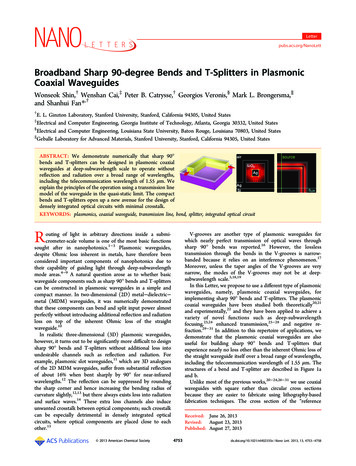
Nano LettersLetterFigure 1. Structures of a sharp 90 bend and T-splitter in plasmoniccoaxial waveguides. (a and b) Structures of a bend and T-splitter withthe propagation directions of light indicated by red arrows. (c) Crosssection of the reference plasmonic coaxial waveguide. Silver is used asthe metal, but it is substituted by perfect electric conductor (PEC) toillustrate some of the physics.Figure 2. Properties of the reference waveguide. (a) Dispersionrelations of the fundamental modes of the reference waveguides madeof silver and PEC. The data points are obtained from the FDFD modesolver.11,36 The blue solid line is the light line in silica, and itsalignment with the blue open dots proves the accuracy of the modesolver results. The red open dots and cross hairs are for the waveguideswith 25-nm-thick and infinitely thick outer silver layers, respectively,and their coincidence proves the effectiveness of the 25-nm-thick outersilver layer. The red dashed line connects the origin and the data pointfor λ0 1.55 μm, for which the guide wavelength is λg 0.68 μm, andits alignment with the red open dots shows that the mode is quasiTEM. The propagation length11 for λ0 1.55 μm is Lp 6.82 μm. (band c) Magnitudes (colors) and directions (arrows) of the transverseE- and H-fields of the fundamental mode of the reference waveguidemade of silver for λ0 1.55 μm. The longitudinal components are notshown because they are much smaller than the transverse components.The dielectric constants of silicon,37 silica,37 and silver34 are takenfrom tabulated data.waveguide” examined in this Letter is described in Figure 1c.The waveguide is placed on top of a silicon (Si) substrate, andthe space between inner and outer coaxial metals is filled withsilica (SiO2). Throughout this Letter, we use silver (Ag) as themetal. We also use the perfect electric conductor (PEC) toillustrate some of the physics. The choice of the metal used willbe specified explicitly for each numerical result.To study the properties of the reference waveguide as well asthe bends and splitters implemented in it, we use the 3D finitedifference frequency-domain (FDFD) method to solveMaxwell’s equations numerically for each vacuum wavelengthλ0.32,33 The FDFD method allows us to use tabulated dielectricconstants of dispersive materials such as silver34 directly,including both the real and the imaginary parts. For accurateyet efficient solution, we use nonuniform spatial grids whosecells are as small as 1 nm inside the waveguide region and aslarge as 20 nm further outside. To simulate infinitely longwaveguides, we surround the entire simulation domain by thestretched-coordinate perfectly matched layer (SC-PML), which,for frequency-domain solvers, was proven to be much superiorto the more commonly used uniaxial PML.35The fundamental mode of the reference waveguide made ofsilver is a quasi-transverse-electromagnetic (quasi-TEM) mode.The quasi-TEM mode inherits many desirable properties of thetrue TEM mode of the same coaxial waveguide made ofPEC.11,20 First, it has a nearly linear dispersion relation asshown in Figure 2a. Therefore, the waveguide has a nearlyconstant group velocity over a broad range of wavelengths andhas no cutoff wavelength; the latter means that it can guide lightwith wavelengths much larger than the cross-sectionaldimensions of the coaxial waveguide. Second, the E- and Hfields of the quasi-TEM mode are tightly confined between thetwo metals, as shown in Figure 2b and c for a vacuumwavelength λ0 1.55 μm. Remarkably, we find that only a 25nm-thick outer metal layer is sufficient for confining the fieldswithin the waveguide, because the opposite electric charges andcurrents carried by the inner and outer metals cancel the fieldsoutside the coaxial waveguide efficiently. Note that the area ofthe silica region, where most of the fields are confined, is lessthan (1.55 μm/10)2, which is at deep-subwavelength scale forthe vacuum wavelength λ0 1.55 μm. In fact, because of theabove-mentioned field cancellation effect, the area of confinement stays almost the same even if λ0 increases from 1.55 μm,so the confinement becomes even stronger for longerwavelengths.Now, we examine the performance of the sharp 90 bend inthe reference waveguide made of silver shown in Figure 1a. Foreach vacuum wavelength λ0 between 1 and 5 μm, we excite thefundamental mode of the waveguide by an electric currentsource plane located 0.5 μm before the bend; in reality thefundamental mode can be excited by coupling the lowest-ordertransverse magnetic (TM01) mode of optical fibers38 or thequasi-TEM mode of plasmonic coaxial lasers.39 We thenmeasure the transmitted power through a flux plane located 0.5μm after the bend.Figures 3a and b shows the solutions of Maxwell’s equationsfor such measurement for λ0 1 μm and λ0 1.55 μm; noticethat for λ0 1 μm a strong standing wave pattern is formed in4754dx.doi.org/10.1021/nl402335x Nano Lett. 2013, 13, 4753 4758
Nano LettersLetterthe quasi-static limit also occurs in a bend in the referencewaveguide made of PEC as shown in Figure 3c, which isconsistent with the result in the classical microwave literature.41Figure 4. Performance of the sharp 90 bend in the PEC coaxialwaveguide with various cross-sectional dimensions. The parameters aand b are indicated in the inset figure. The transmittance is measuredwhile varying a for b 50 nm (open dots), varying b for a 150 nm(solid dots), and varying b for a b 20 nm (cross hairs). Note thatthe high transmittance for b 50 nm is not very sensitive to thevariation of a. On the other hand, the variation of b affects thetransmittance significantly.Figure 3. Performance of the sharp 90 bend. (a and b) Plots of theamplitude of the H-field component normal to the plane containingthe axes of the input and output waveguides for λ0 1 μm and λ0 1.55 μm. Silver is used as the metal. The distances from the center ofthe junction to the electric current source plane (green) and the fluxmeasurement plane (cyan) are both 0.5 μm. Notice the strongstanding wave pattern in the input waveguide in (a) due to significantreflection of the input wave at the junction. (c) Transmittance spectrathrough the bend. The transmittance is higher for the PEC waveguidethan the silver waveguide, but both converge to 100% as the vacuumwavelength λ0 increases. For the silver waveguide, T 97.5% isobtained at λ0 1.55 μm. The nearly perfect transmission is achievedfor λ0 1.55 μm, a broad range of wavelengths; note that thehorizontal axis is on a logarithmic scale.We note that the nearly perfect transmission is a broadbandphenomenon achieved from λ0 1.55 μm to mid-infrared,because the quasi-static approximation applies to anysufficiently long wavelengths. The closed structure of thecoaxial waveguide that prohibits coupling with other leakagechannels such as radiation is crucial for the nearly perfecttransmission; in other conventional 3D plasmonic waveguidesthat are open to the leakage channels, the transmission does notbecome perfect in the quasi-static limit because additional lossinto the leakage channels is unavoidable.Even though the quasi-static approximation holds in generalwhen the cross-sectional dimensions of the coaxial waveguideare much smaller than the wavelength, we find that the size ofthe inner metal is the most critical among all cross-sectionaldimensions. In Figure 4, we measure the transmittance throughthe PEC coaxial waveguide bend for a vacuum wavelength λ0 1.55 μm as varying cross-sectional dimensions of the waveguidewhile maintaining one of the following three parameters thesame: a, b, and a b (see the inset of Figure 4). The figureshows that the transmittance stays high as long as b is muchsmaller than the wavelength, whereas it decreases fast as bincreases even if the other two parameters are at deepsubwavelength scale. The strong impact of b, that is, the size ofthe inner metal, on the transmittance can be explained by theelectromagnetic field distributions of the waveguide modeshown in Figure 2b and c: the fields are strongest near the innermetal, so the size of the inner metal is likely to affecttransmission properties significantly. We note, however, thatthe nearly perfect transmission is still quite tolerant of thechanges in parameter values; for example, when b changes by10% from 50 nm, the transmittance stays above 98% for both a 150 nm and a b 20 nm.Next, we examine the performance of the T-splitter in thereference waveguide made of silver shown in Figure 1b. By thethe input waveguide by the interference between the input andreflected waves, whereas for λ0 1.55 μm the pattern isdiminished significantly, which means that most of the inputpower is transmitted through the bend without reflection. Weperform a similar measurement of the power transmitted over(0.5 0.5) μm in a straight waveguide. The ratio of themeasurement in the bend with respect to the measurement inthe straight waveguide is the transmittance of the bend. Such adefinition of transmittance is intended to capture loss that isadded on top of the propagation loss of the straight waveguide;the additional loss can be due to additional Ohmic lossintroduced by the bend or due to reflection and radiation lossat the bend.The measured transmittance is shown as a spectrum inFigure 3c. It shows that the transmittance approaches 100% asthe wavelength increases. Especially, a transmittance of 97.5% isachieved for λ0 1.55 μm without any optimization of thegeometry of the bend. This remarkable phenomenon can beexplained as follows. For wavelengths much larger than thecross-sectional dimensions of the waveguide, the quasi-staticapproximation applies, and hence the junction between theinput and output waveguides at the bend can be accuratelymodeled as a junction between two transmission lines.40Because the input and output waveguides have the same crosssectional shape, the two transmission lines have the samecharacteristic impedance. Therefore, the transmittance shouldbe 100% in the quasi-static limit. The perfect transmission in4755dx.doi.org/10.1021/nl402335x Nano Lett. 2013, 13, 4753 4758
Nano LettersLetterFigure 5. Performance of the T-splitter. (a) Transmittance into one ofthe two output waveguides of the splitter shown in Figure 1b. Silver isused as the metal. Both the output waveguides are the referencewaveguides, while the input waveguide is either the reference or theoptimal (see Figure 6) waveguide. For the reference input waveguidethe transmittance reaches 44.4% as the vacuum wavelength λ0increases, whereas for the optimal input waveguide it reaches theideal 50.0% over a broad range of wavelengths of λ0 1.55 μm; notethat the horizontal axis is on a logarithmic scale. (b) Flow of electriccurrent in the T-junction, in which the three reference waveguides aremodeled as three transmission lines with the same characteristicimpedance Z0. When the voltage difference Vin is applied between theinner and outer metals, the current I is launched in the inputwaveguide and equally divided into the two output waveguides at thejunction. Note that the three seemingly separate outer metal piecesshown in the figure are actually a single connected outer metal layer.same method used for the bend, we measure the transmittancethrough one of the two output waveguides. An ideal splittershould transmit 50% of the input power into each outputwaveguide. However, for the splitter shown in Figure 1b forwhich the input and output waveguides have the same crosssectional shape, it turns out that the transmittance reaches only44.4% even for long wavelengths as shown in Figure 5a. Thisasymptotic value of the transmittance can be also explained bymodeling the T-junction as a junction between threetransmission lines in the quasi-static limit. Because all of thethree waveguides connected at the T-junction have the samecross-sectional shape, the characteristic impedance Zin of theinput transmission line and Zout of each of the two outputtransmission lines have the same value Z0, that is, Zin Zout Z0. The two output transmission lines form a parallelcombination of impedances with respect to the inputtransmission line, because the current flowing through theinput transmission line is equally divided into the two outputtransmission lines as indicated in Figure 5b. Therefore, the loadimpedance seen by the input transmission line is ZL Zout/2,and the reflectance is calculated asR ZL Z in 2ZL Z in2 Z0/2 Z0 2Z0/2 Z02 1.9Figure 6. Optimization of the T-splitter. (a) Structure of the T-splitteron the vertical cross section containing the axis of the input waveguide.The inner metal size bin of the input waveguide is increased from theoriginal size 50 nm to eliminate the reflection of the input wave at theT-junction. The red arrow and bullseye indicate the propagationdirection of light. (b) Spectra of the actual reflectance in the 3D FDFDsolution of Maxwell’s equations (open dots) and the reflectancepredicted by the transmission line model (solid dots) for the T-splitterin the silver coaxial waveguide. The actual reflectance almost vanishesfor bin 90 nm, but the transmission line model slightlyunderestimates the optimal bin. (c) Similar spectra for the T-splitterin the PEC coaxial waveguide, but the prediction by the transmissionline model is made using the analytic formula of the characteristicimpedance of the PEC coaxial waveguide. (d and e) Amplitude of theH-field component normal to the plane containing the axes of theinput and output waveguides of the splitters with the reference (bin 50 nm) and optimal (bin 90 nm) input waveguides. Only a half of thesplitter is shown by virtue of the mirror symmetry. Silver is used as themetal, and the distances from the center of the junction to the electriccurrent source plane (green) and the flux measurement plane (cyan)are both 0.5 μm. Notice the strong standing wave pattern in (d) due tosignificant reflection of the input wave at the T-junction.It is important to emphasize that the plasmonic coaxialwaveguides and 2D MDM waveguides have very differenttopologies in their transmission line models for the T-splitters,despite a close connection between these two classes ofwaveguides in terms of the modal properties of the straightwaveguides.21To eliminate the reflection, we decrease Zin gradually byincreasing the size bin of the inner metal of the input waveguideas described in Figure 6a and measure the reflectance for λ0 1.55 μm. Figure 6b shows that indeed the reflection almostvanishes for bin 90 nm, for which the reflectance is only0.17%. We note that the nearly vanishing reflection is quitetolerant of the change in bin; for example, even if bin changes by10% from the optimal value, the reflectance stays below 2%.(1)The remaining 1 R portion of the input power that is notreflected should be equally divided into each output transmission line, because no leakage channels such as radiation arecoupled at the junction. Therefore, the transmittance into eachoutput transmission line should be T (1 R)/2 4/9 44.4% in the quasi-static limit, which is exactly the asymptoticvalue in Figure 5a.Equation 1 suggests one way of eliminating the reflection,which is to decrease Zin from Z0 to Z0/2. We note that for the Tsplitter in the 2D MDM waveguide the recipe was opposite,that is, to increase Zin, because the two output waveguidesformed a series rather a parallel combination of impedances.104756dx.doi.org/10.1021/nl402335x Nano Lett. 2013, 13, 4753 4758
Nano LettersLettersophisticated methods utilizing silver nanowire bends49,50 anddielectric-coated silver nanowires.51 53 Another interestingapproach is to use metal-coated semiconductor nanowires54,55as conductive inner pieces of plasmonic coaxial waveguides;because the semiconductor nanowires can be grown intovarious structures such as bends,56 branches,57,58 and combs,59they can be useful for building networks of plasmonic coaxialwaveguides. We believe that our theoretical study will inspirefurther experimental works on actual fabrication and characterization of complex optical circuits based on plasmonicwaveguides.Figure 6d and e shows the solutions of Maxwell’s equations forbin 50 nm and bin 90 nm for λ0 1.55 μm. Notice thepresence of a strong standing wave pattern in the inputwaveguide in Figure 6d and the absence of such a standingwave pattern in Figure 6e, which confirms that the choice of bin 90 nm indeed results in nearly perfect transmission.Even though the splitter is optimized for λ0 1.55 μm, thesame splitter turns out to exhibit nearly perfect transmissionover a broad range of wavelengths spanning from λ0 1.55 μmto mid-infrared as shown in Figure 5a. The broadband perfecttransmission is also explained by the transmission line model asfollows. Because the mode of each plasmonic coaxial waveguideis quasi-TEM, its characteristic impedance is nearly independent of wavelength. Therefore, for sufficiently long wavelengthsfor which the transmission line model holds, eq 1 predicts thenearly constant transmittance, which is T 50% for theoptimized splitter.To assess the validity of the transmission line model morequantitatively, we predict the reflectance by substitutingnumerically calculated impedances Z in the formula for R ineq 1; Z is calculated as V/I, where the voltage difference Vbetween the inner and the outer metals and the electric currentI flowing through the inner metal are calculated by numericallyintegrating the E- and H-fields of the fundamental mode of thewaveguide.12,42 In Figure 6b, the predicted reflectance iscompared with the actual reflectance in the 3D FDFD solutionof Maxwell’s equations. In Figure 6c we make a similarcomparison between the predicted and actual reflectances forthe splitter in the PEC coaxial waveguide, for which the analyticexpression for Z exists.43 46 For both the silver and the PECcoaxial waveguides, the prediction from the transmission linemodel correctly describes the overall trend of the actualreflectance as a function of bin, but we find that the modelslightly underestimates the optimal bin for vanishing reflectance.In addition to its dependence on the impedances of the inputand output waveguides, the reflectance also depends on thedetailed shape of the junction between the input and outputwaveguides: it turns out that the reflectance does not reduce tozero unless the thicker inner metal of the input waveguideextends into the junction and reaches the central axis of theoutput waveguide as shown in Figure 6a. Such dependence onthe detailed shape of the junction is of course not incorporatedin the simple transmission line model above. Following theliterature of microwave circuits one could develop a moresophisticated model that includes additional lumped circuitelements47,48 to describe the properties of the junction moreaccurately. Nevertheless, as we can see here the simple modelabove does provide very important guidance for the overalldesign of the T-splitter.In conclusion, we have proposed and analyzed compact andrealistic designs of sharp 90 bends and T-splitters in plasmoniccoaxial waveguides, which can be useful in delivering opticalsignals into a submicrometer-scale volume such as a nanophotonic detector. The bends and splitters transmit opticalwaves nearly perfectly without parasitic reflection and radiation,so they help to minimize undesirable crosstalk in integratedoptical circuits. Also, because the nearly perfect transmissionoccurs over a broad range of wavelengths, the performance ofour bends and splitters should be tolerant of fabrication errors,thermal expansion, and wavelength detuning than previouslyproposed bend and splitter designs based on interference andresonance. The proposed designs can be fabricated either bystandard lithography-based fabrication methods, or by more AUTHOR INFORMATIONCorresponding Author*E-mail: shanhui@stanford.edu.NotesThe authors declare no competing financial interest. ACKNOWLEDGMENTSThis work was supported by the National Science Foundation(Grant No. DMS 09-68809), the MARCO Interconnect FocusCenter, and the AFOSR MURI programs (Grant Nos. FA955009-1-0704 and FA9550-12-1-0024). W.S. also acknowledges thesupport of Samsung Scholarship. REFERENCES(1) Joannopoulos, J. D.; Johnson, S. G.; Winn, J. N.; Meade, R. D.Photonic Crystals: Molding the Flow of Light, 2nd ed.; PrincetonUniversity Press: Princeton, NJ, 2008.(2) Manolatou, C.; Johnson, S. G.; Fan, S.; Villeneuve, P. R.; Haus,H. A.; Joannopoulos, J. D. J. Lightwave Technol. 1999, 17, 1682 1692.(3) Miller, D. A. B. Proc. IEEE 2000, 88, 728 749.(4) Barnes, W. L.; Dereux, A.; Ebbesen, T. W. Nature 2003, 424,824 830.(5) Ozbay, E. Science 2006, 311, 189 193.(6) Maier, S. IEEE J. Sel. Top. Quantum Electron. 2006, 12, 1671 1677.(7) Oulton, R. F.; Sorger, V.; Genov, D.; Pile, D. F. P.; Zhang, X. Nat.Photonics 2008, 2, 496 500.(8) Brongersma, M. L.; Shalaev, V. M. Science 2010, 328, 440 441.(9) Gramotnev, D. K.; Bozhevolnyi, S. I. Nat. Photonics 2010, 4, 83 91.(10) Veronis, G.; Fan, S. Appl. Phys. Lett. 2005, 87, 131102.(11) Veronis, G.; Fan, S. J. Lightwave Technol. 2007, 25, 2511 2521.(12) Cai, W.; Shin, W.; Fan, S.; Brongersma, M. L. Adv. Mater. 2010,22, 5120 5124.(13) Liu, L.; Han, Z.; He, S. Opt. Express 2005, 13, 6645 6650.(14) Shin, W.; Raman, A.; Fan, S. J. Opt. Soc. Am., B 2012, 29, 1048 1054.(15) Veronis, G.; Fan, S. Opt. Express 2008, 16, 2129 2140.(16) Pile, D. F. P.; Gramotnev, D. K. Opt. Lett. 2005, 30, 1186 1188.(17) Volkov, V. S.; Bozhevolnyi, S. I.; Devaux, E.; Ebbesen, T. W.Appl. Phys. Lett. 2006, 89, 143108.(18) Pile, D. F. P.; Gramotnev, D. K. Opt. Lett. 2004, 29, 1069 1071.(19) Moreno, E.; Garcia-Vidal, F. J.; Rodrigo, S. G.; Martin-Moreno,L.; Bozhevolnyi, S. I. Opt. Lett. 2006, 31, 3447 3449.(20) Baida, F. I.; Belkhir, A.; Van Labeke, D.; Lamrous, O. Phys. Rev.B 2006, 74, 205419.(21) Catrysse, P. B.; Fan, S. Appl. Phys. Lett. 2009, 94, 231111.(22) de Waele, R.; Burgos, S. P.; Polman, A.; Atwater, H. A. NanoLett. 2009, 9, 2832 2837.(23) Rusina, A.; Durach, M.; Nelson, K. A.; Stockman, M. I. Opt.Express 2008, 16, 18576 18589.(24) Weber-Bargioni, A.; Schwartzberg, A.; Cornaglia, M.; Ismach,A.; Urban, J. J.; Pang, Y.; Gordon, R.; Bokor, J.; Salmeron, M. B.;4757dx.doi.org/10.1021/nl402335x Nano Lett. 2013, 13, 4753 4758
Nano LettersLetterOgletree, D. F.; Ashby, P.; Cabrini, S.; Schuck, P. J. Nano Lett. 2011,11, 1201 1207.(25) Moreau, A.; Granet, G.; Baida, F. I.; Van Labeke, D. Opt. Express2003, 11, 1131 1136.(26) Baida, F. I.; Van Labeke, D.; Granet, G.; Moreau, A.; Belkhir, A.Appl. Phys., B: Lasers Opt. 2004, 79, 1 8.(27) Baida, F. I. Appl. Phys., B: Lasers Opt. 2007, 89, 145 149.(28) Rybczynski, J.; Kempa, K.; Herczynski, A.; Wang, Y.; Naughton,M. J.; Ren, Z. F.; Huang, Z. P.; Cai, D.; Giersig, M. Appl. Phys. Lett.2007, 90, 021104.(29) Rodríguez-Fortuño, F. J.; García-Meca, C.; Ortuño, R.; Martí, J.;Martínez, A. Opt. Lett. 2009, 34, 3325 3327.(30) Burgos, S. P.; de Waele, R.; Polman, A.; Atwater, H. A. Nat.Mater. 2010, 9, 407 412.(31) de Waele, R.; Burgos, S. P.; Atwater, H. A.; Polman, A. Opt.Express 2010, 18, 12770 12778.(32) Veronis, G.; Fan, S. In Surface Plasmon Nanophotonics;Brongersma, M., Kik, P., Eds.; Springer: Dordrecht, Netherlands,2007; pp 169 182.(33) Shin, W.; Fan, S. Opt. Express 2013, 21, 22578 22595.(34) Lide, D. R., Ed. CRC Handbook of Chemistry and Physics, 88thed.; CRC Press: Boca Raton, FL, 2007.(35) Shin, W.; Fan, S. J. Comput. Phys. 2012, 231, 3406 3431.(36) Pereda, J. A.; Vegas, A.; Prieto, A. Microwave Opt. Technol. Lett.2003, 38, 331 335.(37) Palik, E. D., Ed. Handbook of Optical Constants of Solids;Academic Press: San Diego, CA, 1985.(38) Ramachandran, S.; Kristensen, P.; Yan, M. F. Opt. Lett. 2009, 34,2525 2527.(39) Khajavikhan, M.; Simic, A.; Katz, M.; Lee, J. H.; Slutsky, B.;Mizrahi, A.; Lomakin, V.; Fainman, Y. Nature 2012, 482, 204 207.(40) Marcuvitz, N. Waveguide Handbook; The Institution ofEngineering and Technology: London, U.K., 2009.(41) Navarro, E. A.; Wu, C.; Chung, P. Y.; Litva, J. Microwave Opt.Technol. Lett. 1995, 8, 138 140.(42) Huang, J. S.; Feichtner, T.; Biagioni, P.; Hecht, B. Nano Lett.2009, 9, 1897 1902.(43) Conning, S. W. IEEE Trans. Microwave Theory Tech. 1964, 12,468 468.(44) Anderson, G. M. Trans. Am. Inst. Elect. Eng. 1950, 69, 728 731.(45) Bowman, F. Introduction to Elliptic Functions with Applications;Dover: New York, 1961.(46) Wadel, B. C. Transmission Line Design Handbook; Artech House:Norwood, MA, 1991; Sec. 3.2.4.(47) Montgomery, C. G., Dicke, R. H., Purcell, E. M., Eds. Principlesof Microwave Circuits; McGraw-Hill: New York, 1948; Sec. 9.6.(48) Garg, R. In Encyclopedia of RF and Microwave Engineering;Chang, K., Ed.; John Wiley & Sons: Hoboken, NJ, 2005; pp 653 658.(49) Sanders, A. W.; Routenberg, D. A.; Wiley, B. J.; Xia, Y.;Dufresne, E. R.; Reed, M. A. Nano Lett. 2006, 6, 1822 1826.(50) Wang, W.; Yang, Q.; Fan, F.; Xu, H.; Wang, Z. L. Nano Lett.2011, 11, 1603 1608.(51) Yin, Y.; Lu, Y.; Sun, Y.; Xia, Y. Nano Lett. 2002, 2, 427 430.(52) Sun, X.; Li, Y. Adv. Mater. 2005, 17, 2626 2630.(53) Luo, L.-B.; Yu, S.-H.; Qian, H.-S.; Zhou, T. J. Am. Chem. Soc.2005, 127, 2822 2823.(54) Fang, Y. J.; Sha, S.; Wang, Z. L.; Wan, Y. T.; Xia, W. W.; Wang,Y. W. Appl. Phys. Lett. 2011, 98, 033103.(55) Pyne, S.; Sahoo, G. P.; Bhui, D. K.; Bar, H.; Sarkar, P.; Samanta,S.; Maity, A.; Misra, A. Spectrochim. Acta, Part A: M
The fundamental mode of the reference waveguide made of silver is a quasi-transverse-electromagnetic (quasi-TEM) mode. The quasi-TEM mode inherits many desirable properties of the true TEM mode of the same coaxial waveguide made of PEC.11,20 First, it has a nearly linear dispersion relation as shown in Figure 2a. Therefore, the waveguide has a .