Transcription
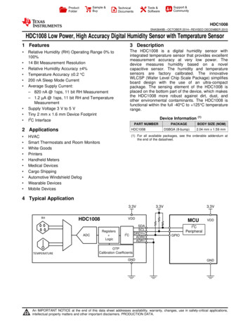
Sample &BuyProductFolderTools &SoftwareTechnicalDocumentsSupport &CommunityHDC1008SNAS649B – OCTOBER 2014 – REVISED DECEMBER 2015HDC1008 Low Power, High Accuracy Digital Humidity Sensor with Temperature Sensor1 Features3 Description The HDC1008 is a digital humidity sensor withintegrated temperature sensor that provides excellentmeasurement accuracy at very low power. Thedevice measures humidity based on a novelcapacitive sensor. The humidity and temperaturesensors are factory calibrated. The innovativeWLCSP (Wafer Level Chip Scale Package) simplifiesboard design with the use of an ultra-compactpackage. The sensing element of the HDC1008 isplaced on the bottom part of the device, which makesthe HDC1008 more robust against dirt, dust, andother environmental contaminants. The HDC1008 isfunctional within the full -40 C to 125 C temperaturerange.1 Relative Humidity (RH) Operating Range 0% to100%14 Bit Measurement ResolutionRelative Humidity Accuracy 4%Temperature Accuracy 0.2 C200 nA Sleep Mode CurrentAverage Supply Current:– 820 nA @ 1sps, 11 bit RH Measurement– 1.2 µA @ 1sps, 11 bit RH and TemperatureMeasurementSupply Voltage 3 V to 5 VTiny 2 mm x 1.6 mm Device FootprintI2C InterfaceDevice InformationPART NUMBERPACKAGE(1)BODY SIZE (NOM)2 ApplicationsHDC1008 (1) For all available packages, see the orderable addendum atthe end of the datasheet.HVACSmart Thermostats and Room MonitorsWhite GoodsPrintersHandheld MetersMedical DevicesCargo ShippingAutomotive Windshield DefogWearable DevicesMobile DevicesDSBGA (8-bump)2.04 mm x 1.59 mm4 Typical egisters OTPCalibration CoefficientsGNDGND1An IMPORTANT NOTICE at the end of this data sheet addresses availability, warranty, changes, use in safety-critical applications,intellectual property matters and other important disclaimers. PRODUCTION DATA.
HDC1008SNAS649B – OCTOBER 2014 – REVISED DECEMBER 2015www.ti.comTable of Contents12345678Features .Applications .Description .Typical Application .Revision History.Pin Configuration and Functions 45667Absolute Maximum Ratings .ESD Ratings.Recommended Operating Conditions.Thermal Information .Electrical Characteristics.I2C Interface Electrical Characteristics.I2C Interface Timing Requirements .Typical Characteristics .Detailed Description . 98.1 Overview . 98.2 Functional Block Diagram . 98.3 Feature Description. 98.4 Device Functional Modes. 98.5 Programming. 108.6 Register Map . 149Application and Implementation . 169.1 Application Information. 169.2 Typical Application . 169.3 Do's and Don'ts . 1810 Power Supply Recommendations . 1811 Layout. 1911.1 Layout Guidelines . 1911.2 Layout Example . 2112 Device and Documentation Support . 2212.112.212.312.412.5Documentation Support .Community Resources.Trademarks .Electrostatic Discharge Caution .Glossary .222222222213 Mechanical, Packaging, and OrderableInformation . 225 Revision HistoryChanges from Revision A (November 2014) to Revision BPage Deleted references to functional and operating temperature ranges. . 1 Changed wording to clarify . 3 Moved Storage Temperature to Abs Max Rating Table . 4 Changed Handling Ratings table to ESD Ratings table. . 4 Added separate conditions for RH . 4 Added RH condition . 5 Added figure reference. . 5 Added condition . 5 Changed wording to clarify hysteresis definition . 5 Changed recommended operating range . 5 Changed register reference for supply voltage monitoring. The original reference was incorrect . 9 Added recommendation for recovery from soldering. . 18Changes from Original (October 2014) to Revision APage Changed Datasheet's title . 1 Changed description. 1 Changed overview . 9 Changed application information . 16 Changed recovery from soldering . 182Submit Documentation FeedbackCopyright 2014–2015, Texas Instruments IncorporatedProduct Folder Links: HDC1008
HDC1008www.ti.comSNAS649B – OCTOBER 2014 – REVISED DECEMBER 20156 Pin Configuration and FunctionsWLCSP (DSBGA)8 Pin YPATop ViewA2B1B2C1D1RHSENSORA1C2D2Pin FunctionsPINI/O TYPE (1)DESCRIPTIONNAMENO.SCLA1ISerial clock line for I2C, open-drain; requires a pull-up resistor to VDDVDDB1PSupply VoltageADR0C1IAddress select pin – hardwired to GND or VDDADR1D1IAddress select pin – hardwired to GND or VDDSDAA2I/OSerial data line for I2C, open-drain; requires a pull-up resistor to VDDGNDB2GGroundDNCC2-Do Not Connect, or may be connected to GNDDRDYnD2OData ready, active low, open-drain, requires a pull-up resistor to VDD. If not used tie to GND.(1)P Power, G Ground, I Input, O OutputSubmit Documentation FeedbackCopyright 2014–2015, Texas Instruments IncorporatedProduct Folder Links: HDC10083
HDC1008SNAS649B – OCTOBER 2014 – REVISED DECEMBER 2015www.ti.com7 Specifications7.1 Absolute Maximum Ratings (1)Input VoltageStorage Yn-0.36ADR0-0.3VDD 0.3ADR1-0.3VDD 0.3-65150TSTG(2)UNITV CStresses beyond those listed under Absolute Maximum Ratings may cause permanent damage to the device. These are stress ratingsonly, which do not imply functional operation of the device at these or any other conditions beyond those indicated under RecommendedOperating Conditions. Exposure to absolute-maximum-rated conditions for extended periods may affect device reliability.For long term storage, it is recommended to stay within 10%RH-80%RH and 5 C to 60 C. Storage beyond this range may result in atemporary RH offset shift.7.2 ESD RatingsVALUEV(ESD)(1)(2)Electrostatic dischargeHuman body model (HBM), per ANSI/ESDA/JEDEC JS-001, allpins (1) 1000Charged device model (CDM), per JEDEC specification –500 500JESD22-C101, all pins (2) 250UNITVJEDEC document JEP155 states that 500-V HBM allows safe manufacturing with a standard ESD control process.JEDEC document JEP157 states that 250-V CDM allows safe manufacturing with a standard ESD control process.7.3 Recommended Operating Conditionsover operating range (unless otherwise noted)MINNOMMAXVDDSupply Voltage2.735.5UNITVTA, TemperatureSensorAmbient Operating Temperature-40125 CTA, HumiditySensorAmbient Operating Temperature-2060 C7.4 Thermal InformationHDC1008THERMAL METRIC(1)DSBGA (YPA)UNIT8 PINSRθJA(1)4Junction-to-Ambient Thermal Resistance98.0 C/WFor more information about traditional and new thermal metrics, see the: IC Package Thermal Metrics application report, SPRA953.Submit Documentation FeedbackCopyright 2014–2015, Texas Instruments IncorporatedProduct Folder Links: HDC1008
HDC1008www.ti.comSNAS649B – OCTOBER 2014 – REVISED DECEMBER 20157.5 Electrical CharacteristicsThe electrical ratings specified in this section apply to all specifications in this document, unless otherwise noted. TA 30 C,VDD 3V, and RH 40%.PARAMETERTEST CONDITIONMINTYPMAXUNITRH measurement, bit 12 of 0x02 register 0 (1)180220µATemperature measurement, bit 12 of 0x02register 0 (1)155185µASleep Mode110200nAAverage @ 1 measurement/second, RH (11bit), bit 12 of 0x02 register 0 (1) (2)730nAAverage @ 1 measurement/second, Temp(11 bit), bit 12 of 0x02 register 0 (1) (2)580nAAverage @ 1 measurement/second, RH(11bit) temperature (11 bit), bit 12 of 0x02register 1 (1) (2)1.2µAStartup (average on Start-up time)300µAPeak current7.6mAAverage @ 1 measurement/second, RH(11bit) temperature (11 bit), bit 12 of 0x02register 1 (1) (2)57µARefer to Figure 2 in Typical Characteristicssection. 4%RH 0.1%RH 1%RHPOWER CONSUMPTIONIDDSupply CurrentIHEATHeater Current (3)RELATIVE HUMIDITY SENSORRHACCAccuracyRHREPRepeatability (3)RHHYSHysteresis0%RH(4)20% RH 60%(5)RHRTResponse TimeRHCTConversion Time (3)t 63%(6)152.50ms11 bit resolution3.85ms14 bit resolutionRHHOROperating Range (7)RHLTDLong Term Drifts8 bit resolutionNon-condensing6.500ms100 0.5%RH%RH/yrTEMPERATURE SENSORTEMPACCAccuracy (3)TEMPREPRepeatability (3)TEMPCTConversion Time (3)TEMPOROperating Range5 C TA 60 C 0.211 bit accuracy14 bit accuracy(1)(2)(3)(4)(5)(6)(7) 0.4 C3.65ms6.35-40 C 0.1ms125 C2I C read/write communication and pull-up resistors current through SCL, SDA and DRDYn not included.Average current consumption while conversion is in progress.This parameter is specified by design and/or characterization and it is not tested in production.The hysteresis value is the difference between an RH measurement in a rising and falling RH environment, at a specific RH point.Actual response times will vary dependent on system thermal mass and air-flow.Time for the RH output to change by 63% of the total RH change after a step change in environmental humidity.Recommended humidity operating range is 20% to 60% RH. Prolonged operation outside this range may result in a measurementoffset. The measurement offset will decrease after operating the sensor in this recommended operating range.Submit Documentation FeedbackCopyright 2014–2015, Texas Instruments IncorporatedProduct Folder Links: HDC10085
HDC1008SNAS649B – OCTOBER 2014 – REVISED DECEMBER 2015www.ti.com7.6 I2C Interface Electrical CharacteristicsAt TA 30 C, VDD 3V (unless otherwise noted)PARAMETERTEST CONDITIONMINTYPMAXUNIT2I C INTERFACE VOLTAGE LEVELVIHInput High VoltageVILInput Low VoltageVOLOutput Low Voltage0.7xVDDSink current 3mA(1)HYSHysteresisCINInput Capacitance on all digital pins(1)V0.3xVDDV0.4V0.1xVDDV0.5pFThis parameter is specified by design and/or characterization and it is not tested in production.I2C Interface Timing Requirements7.7PARAMETERTEST CONDITIONMINTYPMAXUNIT400kHzI2C INTERFACE VOLTAGE LEVELfSCLClock Frequency10tLOWClock Low Time1.3µstHIGHClock High Time0.6µstSPPulse width of spikes that must besuppressed by the input filter (1)tSTARTDevice Start-up time(1)(2)From VDD 2.7 V to ready for aconversion (1) (2)1050ns15msThis parameter is specified by design and/or characterization and it is not tested in production.Within this interval it is not possible to communicate to the RTFigure 1. I2C Timing6Submit Documentation FeedbackCopyright 2014–2015, Texas Instruments IncorporatedProduct Folder Links: HDC1008
HDC1008www.ti.comSNAS
SNAS649B –OCTOBER 2014–REVISED DECEMBER 2015 www.ti.com 7 Specifications 7.1 Absolute Maximum Ratings(1) MIN MAX UNIT VDD -0.3 6 SCL -0.3 6 SDA -0.3 6 Input Voltage V DRDYn -0.3 6 ADR0 -0.3 VDD 0.3 ADR1 -0.3 VDD 0.3 Storage Temperature TSTG(2)-65 150 C (1) Stresses beyond those listed under Absolute Maximum Ratings may cause permanent damage to the device. These