Transcription
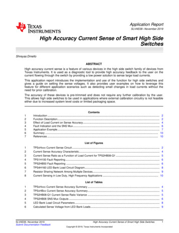
Application ReportSLVAE08 – November 2019High Accuracy Current Sense of Smart High SideSwitchesShreyas DmelloABSTRACTHigh accuracy current sense is a feature of various devices in the high side switch family of devices fromTexas Instruments. It is used as a diagnostic tool to provide high accuracy feedback to the user on thecurrent flowing through the switch by providing a low power solution to sense large load currents.This application report introduces the implementation and use of the function for high side switches andgives a guide on setting the sense voltages. It also provides user examples on how to leverage thisfeature for different application scenarios such as detecting small changes in load currents without theneed for prior calibration.The accuracy of these devices is pre-trimmed and does not require any further calibration by the user.This allows high side switches to be used in applications where external calibration circuitry is not feasibleeither due to increased system level costs or limited packaging space.1234567ContentsIntroduction . 2Function Description . 2Effect of Load Current on Sense Accuracy. 4Fault Indication and the SNS Mux . 6Application Example . 7Summary . 10References . 10List of Figures1TPSxHxxx Current Sense Circuit . 22Current Sense Accuracy Characteristic. 43Current Sense Ratio as a Function of Load Current for TPS2HB08-Q1 . 54TPS1H100 Fault Reporting . 65TPS2HB50 Fault Reporting678. 6TPS4H160 LED Bank Load Circuit Diagram . 8Resistor Sharing Network Among Multiple Devices . 9Current Sensing in Low Duty, High Frequency Applications . 10List of Tables1TPSxHxxx Current Sense Accuracy Summary . 42TPSxHBxx Current Sense Accuracy Summary . 53TPS2HB08-Q1 Current Sense Ratio Variance4TPS2HB08 SNS Mux Outputs . 65LED Bank Load Circuit Parameters . 86Calculated Sense Voltage from LED Bank Loads . 9SLVAE08 – November 2019Submit Documentation Feedback.High Accuracy Current Sense of Smart High Side SwitchesCopyright 2019, Texas Instruments Incorporated51
Introductionwww.ti.comTrademarksAll trademarks are the property of their respective owners.1IntroductionHigh-side switches from Texas Instruments are robust devices that can be used in industrial, automotive,and other power applications. They are rated at 40 V and have a wide range of on-resistance and multichannel configurations to meet the user's needs. The high accuracy current sense enables full diagnosticsincluding current limiting and various other protective features.High accuracy current sensing allows for immediate feedback to the user on the status of the system. As adiagnostic tool, it allows the user to monitor the current flowing into the load while maintaining theefficiency of the system, especially in large load applications by providing a low power solution to monitorhigh load currents. The current sense output can also be used in an analog circuit or can be parsed withthe help of an ADC and microcontroller to implement digital logic.2Function Description2.1TPSxHxxx Current Sense Circuit DescriptionA current mirror is a circuit that is specially designed to copy the current flowing through an active device.Using two MOSFETs, the primary FET current is mirrored in the secondary FET. The primary current andthe copied current are related to each other by a fixed current gain ratio. This ratio is dependent onphysical characteristics of the device and cannot be changed by the user.Figure 1 describes the construction of the current sense circuitry.Figure 1. TPSxHxxx Current Sense Circuit2High Accuracy Current Sense of Smart High Side SwitchesCopyright 2019, Texas Instruments IncorporatedSLVAE08 – November 2019Submit Documentation Feedback
Function Descriptionwww.ti.comA current mirror is integrated in TPSxHxxx devices using a MOSFET-based topology. This circuit is sharedbetween multiple channels and in this situation, the select pins (SELx) choose which channel is mirroredthrough the sense circuitry. The use of a current mirror topology allows for immediate feedback to beprovided to the user without affecting the operation and the efficiency of the high power system. Thesense circuitry has low current flowing through it. This allows the use of a low power solution to sensehigh load currents. The load current and the sense current are related to each other by a fixed gain factorKCS or KSNS, which is referred to as the "Current Sense Ratio" in the device data sheet.Accurate current sensing can be used as a diagnostic tool in circuit design. The goal of the current sensecircuit is to translate the load current into a voltage value that can be measured by sourcing a sensecurrent through an external sense resistor. In the case of a fault, there exists a feedback loop that sourcesa steady fault current or pulls up to a fault voltage depending on which device is used. Therefore, theswitch is able to delineate between fault operation and normal operation. Given the best-in-class accuracywith TI’s high-side switch portfolio, further calibration of the sense circuitry is not needed, savingexpensive production line test costs and complexity.2.2Choosing RSNSAn external resistor must be connected to the CS pin or the SNS pin of the high-side switch. Using thechosen resistor, the user is able to get voltage values in a range that can be parsed depending on theallowed voltages of the ADC or MCU. This voltage value is directly proportional to the amount of loadcurrent flowing through the switch and can be used to implement an off chip fault controller or feedbackcircuitry in the form of a current meter.A resistance value has to be chosen so that the entire load current range can be sensed by the MCU. Alarger resistor has the potential to have greater accuracy since the voltage range gained is larger but thedesigner has to note that the fault condition can cause the sense voltage to reach levels that damage theMCU. To mitigate this, a clamping circuit with a zener diode or a voltage divider circuit can be used ifnecessary.RSNS VSNS ISNS (VSNS KSNS) IOUT(1)Equation 1 describes the calculations that are performed to choose RSNS. Here, VSNS is the nominal voltagevalue chosen by the user for the ADC. This resistor is placed between the SNS pin or CS pin and systemground.To achieve the most accurate current sense value, it is recommended to apply filtering to the SNS output.There are two methods of filtering: Low-Pass RC filter between the SNS pin and the ADC input. Figure 1 illustrates this filter. The typicalrange for the capacitor CSNS is 100 pF to 10 nF. The typical value for the protection resistor RPROT is 15kΩ. The designer must select a CSNS capacitor value based on system requirements. A larger valueprovides improved filtering while a smaller value allows for faster transient response. The ADC and MCU can also be used for filtering. It is recommended that the ADC collects severalmeasurements of the SNS output. The median value of this data set must be considered as the mostaccurate result. By performing this median calculation, the MCU is able to filter out any noise or outlierdata.For example, if a 3.3 V ADC is used and the nominal load current of the system is 1 A, Equation 2describes the calculation for RSNS on the TPS1H100-Q1. A 3 V linear range is chosen to get good currentsense resolution.RSNS (3 500) 1 1.5 kΩ(2)The fault current for the TPS1H100-Q1 is 10 mA. With the chosen resistance, the fault voltage is 15 V.Thus, a zener clamp of 3.3 V and adequate power rating is used to set the fault voltage at 3.3 V, which iswithin specification for the ADC.SLVAE08 – November 2019Submit Documentation FeedbackHigh Accuracy Current Sense of Smart High Side SwitchesCopyright 2019, Texas Instruments Incorporated3
Effect of Load Current on Sense Accuracywww.ti.com3Effect of Load Current on Sense Accuracy3.1Sense Accuracy Trend Over Load CurrentAs load currents are decreased, the accuracy of the current mirror in the sense circuitry decreases. Eventhough certain devices are trimmed to different load current ranges, this trend is present in all TPSxHxxxdevices. The accuracy for different load current ranges is documented in the data sheet and tends to belower for low IOUT. Figure 2 broadly describes the accuracy loss at lower load currents. The load currentand accuracy range are device specific and are stated on the data sheet of every high-side switch.Figure 2. Current Sense Accuracy CharacteristicWhen running the device at lower load currents, concessions need to be made due to the lower senseaccuracy. The sense pin on these devices act as fault indicators when a fault is triggered. The pin sourcesa fault current, ISNSFH, which help differentiate between normal device operation and fault operation. Someissues that can arise due to the loss of accuracy include incorrect ISNSFH sourcing and a current limitovershoot. As such, it is recommended that the designer chooses the high-side switch that is both capableof driving the desired IOUT and also meets the current accuracy requirements of the system. Table 1summarizes the current sense accuracy range of TI high-side switches at various current loads. Detailedaccuracy information is given in the respective data sheets.Table 1. TPSxHxxx Current Sense Accuracy H000-Q14LOAD CURRENTCURRENT SENSE ACCURACYIOUT 5 mA 80%IOUT 50 mA 7%IOUT 1 A 3%IOUT 5 mA 85%IOUT 50 mA 8%IOUT 0.5 A 3%IOUT 5 mA 65%IOUT 50 mA 8%IOUT 0.5 A 3%IOUT 1 mA 50%IOUT 5 mA 10%IOUT 100 mA 2.5%High Accuracy Current Sense of Smart High Side SwitchesCopyright 2019, Texas Instruments IncorporatedSLVAE08 – November 2019Submit Documentation Feedback
Effect of Load Current on Sense Accuracywww.ti.comTable 1. TPSxHxxx Current Sense Accuracy Summary (continued)DEVICELOAD CURRENTCURRENT SENSE ACCURACYIOUT 1 mA 70%IOUT 5 mA 15%IOUT 100 mA 3%TPS4H000-Q1Table 2. TPSxHBxx Current Sense Accuracy Summary3.2Sense Ratio VarianceAs seen in Section 3.1, the load current flowing through the device has a direct effect on the current senseaccuracy. Texas Instruments specs and trims a KCS value for all high-side switches at a fixed load current.In addition to this specification, there is also a ISNSI specification that describes the sense current undervarious load current values. This can be found under Current Sense Characteristics in the ElectricalCharacteristics table of the data sheet. Table 3 describes the sense current variation (ISNSI) for TPS2HB08Q1. The nominal KSNS specified for this device is 5000, which is specified at 1 A of load current.Table 3. TPS2HB08-Q1 Current Sense Ratio VarianceLOAD CURRENTSENSE CURRENTEFFECTIVE KSNSIOUT 10 AISNSI 2.020 mA4950IOUT 3 AISNSI 0.606 mA4950IOUT 1 AISNSI 0.200 mA5000IOUT 300 mAISNSI 0.059 mA5085IOUT 100 mAISNSI 0.0185 mA5405IOUT 50 mAISNSI 0.0084 mA5952To calculate the sense ratio at a load current that has not been specified in the data sheet, linearinterpolation can be used. A straight line can be drawn between the two closest specified current loadsthat bound the application load current. Figure 3 describes the linear interpolation between specified loadcurrents for TPS2HB08-Q1.Current Sense Ratio as a Funtion of Load Current600059005800Sense UT (A)78910CSRaFigure 3. Current Sense Ratio as a Function of Load Current for TPS2HB08-Q1For a load current of x 2 A, a straight line between the data at 1 A and 3 A can be drawn. UsingEquation 3, the current sense ratio can be found.(y - y1) ((y2 - y1)/(x2 - x1)) * (x - x1)(y - 5000) ((4950 - 5000)/(3 - 1)) * (2 - 1)SLVAE08 – November 2019Submit Documentation Feedback(3)(4)High Accuracy Current Sense of Smart High Side SwitchesCopyright 2019, Texas Instruments Incorporated5
Fault Indication and the SNS Muxwww.ti.comy KSNS 49754(5)Fault Indication and the SNS MuxTPSxHBxx high-side switches are a subfamily of TPSxHxxx devices. While they provide similar benefitsand protection, they are built with a different architecture. The main difference between TPSxHBxxdevices and the rest of the TPSxHxxx family is the range of on-resistance offered as well as theimplementation of the external current limiting circuit. TPSxHxxx devices also report a fault on the SNS pinwith an internal pullup that pulls the voltage to VCS(H). This differs from TPSxHBxx devices that output afixed current during fault operation.The SNS pin outputs all the necessary diagnostic information depending on how the SNS Mux isconfigured with the SELx pins. The following faults are communicated via the SNS output: Switch shutdown, due to:– Thermal shutdown– Current limit Active current limiting Open-load/VOUT shorted-to-batteryOpen-load and short-to-battery faults are also indicated when the switch is off and DIAG EN is high.There is an integrated comparator that checks the voltage on the out pin against an internal open-loaddetection threshold, VOL. If VOL VOUT, then there is no fault. If VOL VOUT, then SNS reports a fault.The SNS pin only reports a fault on the selected channel with the SNS Mux. Irrespective of the nature ofthe fault, it is reported by sourcing a fault current, ISNSFH, from the SNS pin. Table 4 describes the outputsof the SNS Mux of the TPS2HB08-Q1 high-side switch. Refer to the device-specific data sheet for otherTPSxHBxx devices for their respective SNS Mux outputs. Version B TPSxHxxx devices do not havededicated status and diagnostic pins. They report faults through the CS pin in a similar method toTPSxHBxx devices.Table 4. TPS2HB08 SNS Mux OutputsINPUTSOUTPUTSDIA ENSEL1SEL2FAULT DETECTSNS0XXXHigh-Z1000CH1 Current1010CH2 Current1100Device Temperature1110N/A1001ISNSFH1011ISNSFH1101Device Temperature1111N/AFigure 4 and Figure 5 describes the fault reporting of the TPS1H100-Q1 and the TPS2HB50, respectively.These graphs describe the fault current loop that the device uses to report a fault. It is recommended toview the device data sheet to confirm the range of the parameters. Considerations such as zener diodeclamps must be used if these voltages reach values that are too high for any external circuitry ormicrocontroller.6High Accuracy Current Sense of Smart High Side SwitchesCopyright 2019, Texas Instruments IncorporatedSLVAE08 – November 2019Submit Documentation Feedback
Application Examplewww.ti.comFigure 4. TPS1H100 Fault Reporting5Application Example5.1LED Driver AccuracyFigure 5. TPS2HB50 Fault ReportingModern lighting solutions are trending toward more LED use. These low power devices have similarluminosity to that of conventional lighting solutions but consume significantly less power. Industrial andautomotive sectors are also moving toward replacing incandescent and halogen lamps with LEDs. SinceLEDs require very low currents to function, current sense accuracy becomes paramount in being able toaccurately sense and protect from fault and open load events.The high side driver topology is popular in the market since it has short to ground and can drive parallelloads. Hence, Texas Instruments offers high-side switches that combine these benefits with high accuracycurrent sense in devices that have a range of on-resistance and output channel configurations. Thisversatility allows the designer to choose the switch that best fits for the application.A common application for high-side switches in the automotive and industrial sector is to drive a bank ofLEDs connected in parallel. The high current sense accuracy allows the system to recognize a fault of oneLED in a large bank, hence, the system can recognize small load current changes. Devices such as theTPS4H160 and TPS4H000 can be used to drive LED banks. Figure 6 shows an example using theTPS4H160.SLVAE08 – November 2019Submit Documentation FeedbackHigh Accuracy Current Sense of Smart High Side SwitchesCopyright 2019, Texas Instruments Incorporated7
Application Examplewww.ti.comFigure 6. TPS4H160 LED Bank Load Circuit DiagramThe accuracy of the current sense feature is dependent on the current pulled by the load and is boundedby the value stated in the data sheet. This bound describes the largest current sense inaccuracy of theswitch. ICS then passes through a chosen resistor, RCS, and VCS is parsed through an ADC. Table 5describes the system constants.Table 5. LED Bank Load Circuit ParametersINPUTSVALUEADCsupply5VRCS2000 ΩRvariance3%KCS300ADCvariance2%ADCleakage3.5 uAADCLSB, tolerance4 LSBInominal, 1 LED60 mAUsing this bound, the load current sense can be calculated by Equation 6.IOUT Inominal (1 - KCS, tolerance 100)(6)The voltage present on the CS pin is also dependant on the accuracy of the resistor used. When thisvoltage is parsed by the ADC, the value read is further affected by its inaccuracy range and the leakagecurrent of the ADC. Equation 7 describes the calculation of the voltage read by the ADC.VCS, read (IOUT (KCS (RCS (1 - Rvariance 100)))) - (ADCleakage (1000 (RCS (1 - Rvariance 100))))(7)The voltage difference between normal operation and fault operation needs to be large enough for theADC to recognize. The difference must result in an LSB drop greater than the LSB tolerance of the ADC.The resolution of the ADC is given by Equation 8.ADCresolution (ADCsupply (1 (ADCvariance 100))) (210 - 1) 1000 4.99 mV/step(8)Table 6 summarizes these calculation for various LED loads in parallel.8High Accuracy Current Sense of Smart High Side SwitchesCopyright 2019, Texas Instruments IncorporatedSLVAE08 – November 2019Submit Documentation Feedback
Application Examplewww.ti.comTable 6. Calculated Sense Voltage from LED Bank LoadsKCS,TOLERANCE8%4%LED LOADINOMINALIREAL1 LED60 mA55.2 mAVCS,350 mV2 LEDs120 mA110.4 mA707 mV5 LEDs300 mA288 mA1.856 V6 LEDs360 mA345.6 mA2.228 VREADΔVCS,READLSB DROP357 mV71 LSBs372 mV74 LSBsHence, high side switches from Texas Instruments have the current sense accuracy to distinguish smallchanges in the load current flowing through the circuit and this change can be correctly reported by astandard ADC.5.2Sense Resistor SharingIn an effort to reduce BOM costs, a microcontroller can be used to run more than one load. This reducesthe number of passive components required in the system, thereby reducing package space as well. Themicrocontroller may not have enough ADC terminals to support a current sense report on every load.Multiple high side switches can use the same sense resistor as shown in Figure 7.Figure 7. Resistor Sharing Network Among Multiple DevicesCertain considerations need to be taken if sense resistor sharing is used. Different load currents perchannel result in different ADC ranges during current sense. Larger load currents on one channel canresult in voltages that are unsafe for the ADC terminal. It is recommended that the sense resistor bechosen for the largest expected load current in the shared network.SLVAE08 – November 2019Submit Documentation FeedbackHigh Accuracy Current Sense of Smart High Side SwitchesCopyright 2019, Texas Instruments Incorporated9
Application Example5.3www.ti.comLow Duty, High Frequency SwitchingSome high power applications can require high frequency switching of the high side switch with a low dutycycle PWM signal. The benefit of using a PWM input allows high power loads to dissipate energy andprovides precise control of the circuit. These applications require a fast settling of the SNS output to beread accurately by an ADC. All TPSxHxxx devices have the sense circuitry settling time defined in theirrespective data sheets.Figure 8 describes a 250 Hz, 5% duty cycle PWM. This signal results in an on-time of only 200 µs. TheADC can sample the SNS output after the defined settling time, tsettle.Figure 8. Current Sensing in Low Duty, High Frequency Applications6SummaryTexas Instruments offers high-side switches with accurate current sensing abilities that can be used as aprotective and diagnostic feature. These devices allow the user to customize the voltage output with thehelp of an external sense resistor.Current sensing is useful for designers in power applications since it can provide immediate feedback tothe designer about the workings of the circuit. As such, this feature benefits designers by eliminating theneed of an external sense circuitry by integrating it into the switch. The current sense circuitry is pretrimmed and calibrated to a high accuracy, allowing easy integration into user designs.7References 10Texas Instruments, Adjustable Current Limit of Smart Power Switches Application ReportHigh Accuracy Current Sense of Smart High Side SwitchesCopyright 2019, Texas Instruments IncorporatedSLVAE08 – November 2019Submit Documentation Feedback
IMPORTANT NOTICE AND DISCLAIMERTI PROVIDES TECHNICAL AND RELIABILITY DATA (INCLUDING DATA SHEETS), DESIGN RESOURCES (INCLUDING REFERENCEDESIGNS), APPLICATION OR OTHER DESIGN ADVICE, WEB TOOLS, SAFETY INFORMATION, AND OTHER RESOURCES “AS IS”AND WITH ALL FAULTS, AND DISCLAIMS ALL WARRANTIES, EXPRESS AND IMPLIED, INCLUDING WITHOUT LIMITATION ANYIMPLIED WARRANTIES OF MERCHANTABILITY, FITNESS FOR A PARTICULAR PURPOSE OR NON-INFRINGEMENT OF THIRDPARTY INTELLECTUAL PROPERTY RIGHTS.These resources are intended for skilled developers designing with TI products. You are solely responsible for (1) selecting the appropriateTI products for your application, (2) designing, validating and testing your application, and (3) ensuring your application meets applicablestandards, and any other safety, security, regulatory or other requirements.These resources are subject to change without notice. TI grants you permission to use these resources only for development of anapplication that uses the TI products described in the resource. Other reproduction and display of these resources is prohibited. No licenseis granted to any other TI intellectual property right or to any third party intellectual property right. TI disclaims responsibility for, and youwill fully indemnify TI and its representatives against, any claims, damages, costs, losses, and liabilities arising out of your use of theseresources.TI’s products are provided subject to TI’s Terms of Sale or other applicable terms available either on ti.com or provided in conjunction withsuch TI products. TI’s provision of these resources does not expand or otherwise alter TI’s applicable warranties or warranty disclaimers forTI products.TI objects to and rejects any additional or different terms you may have proposed. IMPORTANT NOTICEMailing Address: Texas Instruments, Post Office Box 655303, Dallas, Texas 75265Copyright 2022, Texas Instruments Incorporated
It is used as a diagnostic tool to provide high accuracy feedback to the user on the . 4 TPS1H100 Fault Reporting . High Accuracy Current Sense of Smart High Side Switches A current mirror is integrated in TPSxHxxx devices using a MOSFET-based topology. This circuit is shared