Transcription
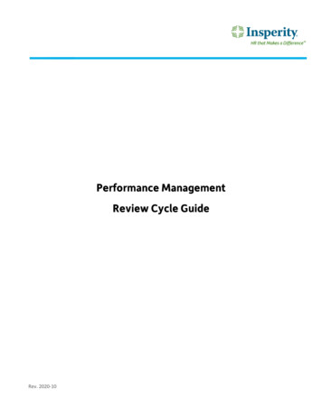
LTC360515V, 5A SynchronousStep-Down RegulatorFEATURESnnnnnnnnnnnnDESCRIPTIONHigh Efficiency: Up to 96%5A Output Current4V to 15V VIN RangeIntegrated Power N-Channel MOSFETs(70mΩ Top and 35mΩ Bottom)Adjustable Frequency 800kHz to 4MHzPolyPhase Operation (Up to 12 Phases)Output Tracking0.6V 1% Reference AccuracyCurrent Mode Operation for Excellent Line and LoadTransient ResponseShutdown Mode Draws Less Than 15µA Supply CurrentAvailable in 24-Pin (4mm 4mm) QFN PackageAEC-Q100 Qualified for Automotive ApplicationsAPPLICATIONSnnnnPoint of Load Power SupplyPortable InstrumentsDistributed Power SystemsBattery-Powered EquipmentThe LTC 3605 is a high efficiency, monolithic synchronousbuck regulator using a phase lockable controlled on-timeconstant frequency, current mode architecture. PolyPhaseoperation allows multiple LTC3605 regulators to run out ofphase while using minimal input and output capacitance.The operating supply voltage range is from 15V down to4V, making it suitable for dual lithium-ion battery inputsas well as point of load power supply applications froma 12V or 5V rail.The operating frequency is programmable from 800kHz to4MHz with an external resistor. The high frequency capability allows the use of small surface mount inductors. Forswitching noise sensitive applications, it can be externallysynchronized from 800kHz to 4MHz. The PHMODE pinallows user control of the phase of the outgoing clocksignal. The unique constant frequency/controlled on-timearchitecture is ideal for high step-down ratio applicationsthat are operating at high frequency while demandingfast transient response. Two internal phase-lock loopssynchronize the internal oscillator to the external clockand also servos the regulator on-time to lock on to eitherthe internal clock or the external clock if it’s present.All registered trademarks and trademarks are the property of their respective owners. Protectedby U.S. patents, including 5481178, 5847554, 6580258, 6304066, 6476589, 6774611.TYPICAL APPLICATIONEfficiency and Power LossHigh Efficiency 1MHz, 5A Step-Down Regulator100VIN 12V90 f 1MHz22µF UN0.1µF 1µH11.5kFBRTITHVOUT3.3V47µF 22.55k16k162k10VOUT 3.3V701VOUT 1.2V605040VOUT 3.3V30VOUT 1.2V0POWER LOSS (W)PVINCLKOUTEFFICIENCY (%)VIN4V TO 15V2010PGND220pF3605 TA01a0101001000OUTPUT CURRENT (mA)0.1100003605 TA01bRev. IDocument FeedbackFor more information www.analog.com1
LTC3605ABSOLUTE MAXIMUM RATINGSPIN CONFIGURATION(Note 1)SVINBOOSTINTVCCSGNDCLKOUTCLKINTOP VIEW24 23 22 21 20 19RT 118 PVINPHMODE 217 PVINMODE 316 SW25PGNDFB 415 SW14 SWITH 613 SWSWSW9 10 11 12PGND8VON7RUNTRACK/SS 5PGOODPVIN, SVIN, SW Voltage. –0.3V to 15VSW Transient Voltage. –2V to 17.5VBOOST Voltage.–0.3V to PVIN INTVCCRUN Voltage. –0.3V to 15VVON Voltage. –0.3V to SVININTVCC Voltage. –0.3V to 3.6VITH, RT, CLKOUT, PGOOD Voltage. –0.3V to INTVCCCLKIN, PHMODE, MODE Voltage. –0.3V to INTVCCTRACK/SS, FB Voltage. –0.3V to INTVCCOperating Temperature Range (Note 2). –40 C to 125 CJunction Temperature (Note 5). 125 CStorage Temperature Range. –65 C to 125 CUF PACKAGE24-LEAD (4mm 4mm) PLASTIC QFNTJMAX 125 C, θJA 37 C/WEXPOSED PAD (PIN 25) IS PGND, MUST BE SOLDERED TO PCBORDER INFORMATIONLEAD FREE FINISHTAPE AND REELPART MARKING*PACKAGE DESCRIPTIONTEMPERATURE RANGELTC3605EUF#PBFLTC3605EUF#TRPBF360524-Lead (4mm 4mm) Plastic QFN–40 C to 85 CLTC3605IUF#PBFLTC3605IUF#TRPBF360524-Lead (4mm 4mm) Plastic QFN–40 C to 125 CAUTOMOTIVE ead (4mm 4mm) Plastic QFN–40 C to 85 CLTC3605IUF#WPBFLTC3605IUF#WTRPBF360524-Lead (4mm 4mm) Plastic QFN–40 C to 125 CContact the factory for parts specified with wider operating temperature ranges. *The temperature grade is identified by a label on the shipping container.Tape and reel specifications. Some packages are available in 500 unit reels through designated sales channels with #TRMPBF suffix.**Versions of this part are available with controlled manufacturing to support the quality and reliability requirements of automotive applications. Thesemodels are designated with a #W suffix. Only the automotive grade products shown are available for use in automotive applications. Contact yourlocal Analog Devices account representative for specific product ordering information and to obtain the specific Automotive Reliability reports forthese models.2Rev. IFor more information www.analog.com
LTC3605ELECTRICAL CHARACTERISTICSThe l denotes the specifications which apply over the full operatingtemperature range, otherwise specifications are at TA 25 C.SYMBOLPARAMETERCONDITIONSMINPVINVIN Supply RangeIQInput DC Supply CurrentActiveShutdown(Note 3)Mode 0, RT 162kVIN 12V, RUN 0VFBFeedback Reference VoltageITH 1.2V (Note 4) –40 C to 85 CITH 1.2V (Note 4) –40 C to 125 CllDVFB(LINE)Feedback Voltage LineRegulationVIN 4V to 15V, ITH 1.2V, –40 C to 85 CVIN 4V to 15V, ITH 1.2V, –40 C to 125 CDVFB(LOAD)Feedback Voltage LoadRegulationITH 0.8V to 1.6V, –40 C to 85 CITH 0.8V to 1.6V, –40 C to 125 CIFBFeedback Pin Input Currentgm (EA)Error Amplifier .3%%ITH 1.2V0.5940.5921.151.35 30nA1.6mStON(MIN)Minimum On-Time40nstOFF(MIN)Minimum Off-Time70nsILIMPositive Inductor Valley Current LimitNegative Inductor Valley Current LimitVFB 0.57VRTOPTop Power NMOS On-ResistanceRBOTTOM6–57.5AAINTVCC 3.3V70150mWBottom Power NMOS On-ResistanceINTVCC 3.3V3555mWVUVLOINTVCC Undervoltage LockoutThresholdINTVCC FallingINTVCC Hysteresis (Rising)2.42.60.252.8VVVRUNRun Threshold 2 (IQ 2mA)Run Threshold 1 (IQ 400µA)RUN RisingRUN Rising1.20.451.250.61.30.75VVVINTVCCInternal VCC Voltage4V VIN 15V3.23.33.4VDVINTVCCINTVCC Load RegulationILOAD 0mA to 20mAOVOutput OvervoltagePGOOD Upper ThresholdVFB Rising71013%UVOutput UndervoltagePGOOD Lower ThresholdVFB Falling–13–10–7%DVFB(HYS)PGOOD HysteresisVFB Returning1.5RPGOODPGOOD Pull-Down Resistance1mA Load120.54V VFB 0.66VIPGOODPGOOD LeakageITRACK/SSTRACK Pull-Up CurrentfOSCOscillator FrequencyCLKINCLKIN Threshold50.5RT 162kl0.85%%25W2µA2.54µA11.2MHz0.7Note 1: Stresses beyond those listed under Absolute Maximum Ratingsmay cause permanent damage to the device. Exposure to any AbsoluteMaximum Rating condition for extended periods may affect devicereliability and lifetime. Absolute Maximum Ratings are those valuesbeyond which the life of a device may be impaired.Note 2: The LTC3605E is guaranteed to meet performance specificationsfrom 0 C to 85 C. Specifications over the –40 C to 85 C operatingtemperature range are assured by design, characterization and correlationwith statistical process controls. The LTC3605I is guaranteed over the full–40 C to 125 C operating temperature range.Note 3: Dynamic supply current is higher due to the internal gate chargebeing delivered at the switching frequency.VNote 4: The LTC3605 is tested in a feedback loop that adjusts VFB toachieve a specified error amplifier output voltage (ITH).Note 5: TJ is calculated from the ambient temperature TA andpower dissipation as follows: TJ TA PD (37 C/W). See ThermalConsiderations section.Note 6: This IC includes overtemperature protection that is intendedto protect the device during momentary overload conditions. Junctiontemperature will exceed 125 C when overtemperature protection is activeContinuous operation above the specified maximum operating junctiontemperature may impair device reliability.Rev. IFor more information www.analog.com3
LTC3605TYPICAL PERFORMANCE CHARACTERISTICS TA 25 C unless otherwise specified.Quiescent Current vs VIN13SHUTDOWN CURRENT N (V)126153069VIN (V)01512RDS(ON) vs Temperature1.5120100INTERNAL ITHCOMPENSATION(ITH 3.3V)1.0TOP FETNORMALIZED (%)60BOTTOM FET402050.544.5VOUTVIN 12V50mV/DIVVOUT 1.2VAC-COUPLEDf 1MHzMODE INTVCCIOUT5A/DIVIL5A/DIVEXTERNAL ITHCOMPENSATION–0.5VIN 12VVOUT 1.2VIOUT 0A TO 5A01243IOUT (A)563605 G04Load Step(Internal ITH Compensation)1.5 2 2.5 3 3.5FREQUENCY (MHz)0–1.530 55 80 105 130TEMPERATURE ( C)1Load Step(External ITH Compensation)–1.00–45 –200.53605 G03Load Regulation8003605 G023605 G01RDS(ON) (mΩ)MODE 3.3VNO LOAD72.022.00IINTVCC Current vs Frequency2514MODE 0VNO LOAD2.16QUIESCENT CURRENT (mA)Shutdown Current vs VINIINTVCC (mA)2.1820µs/DIV3605 G0673605 G05Output TrackingSwitching Frequency vs IN 12VVOUT 3.3VITH 3.3VIOUT 0A TO 5A20µs/DIV3605 G07VIN 12VVOUT 1.2V500µs/DIV3605 G08FREQUENCY (MHz)3.53.02.52.01.51.00.50050 100 150 200 250 300 350 400 450 500RT (kΩ)3605 G094Rev. IFor more information www.analog.com
LTC3605TYPICAL PERFORMANCE CHARACTERISTICS TA 25 C unless otherwise specified.300962001500ILOAD 1A1.29290ILOAD 5ATOP SWITCH408128420160.80.60.20VIN (V)369VIN (V)0151210110010RUN THRESHOLD (V)NORMALIZED INTVCC (%)12141.25989796959493922086VON (V)RUN Pin Threshold vs Temperature994041.30TA 25 C1006023605 G12INTVCC Load RegulationCurrent Limit Foldback1208003605 G113605 G10NORMALIZED MAXIMUM OUTPUT CURRENT (%)1.00.48650Frequency vs VON VoltageVIN 14V1.4 RT 162k881001.6VOUT 3.3V94BOTTOM SWITCH250Efficiency vs VINFREQUENCY (MHz)98EFFICIENCY (%)SWITCH LEAKAGE (nA)Switch Leakage vs VIN3501.201.151.101.0591000.10.20.3 0.4VFB (V)0.50.60.790080 100 120406020INTVCC OUTPUT CURRENT (mA)3605 G131401.00–40–1560358510TEMPERATURE ( C)3605 G153605 G14DCM Operation110CCM VIL2A/DIVIL2A/DIVVIN 12VVOUT 1.2VMODE 0IOUT 0L1 0.33µH400ns/DIV3605 G16VIN 12V400ns/DIVVOUT 1.2VMODE 3.3VPHMODE 3.3VIOUT 0L1 0.33µH3605 G17Rev. IFor more information www.analog.com5
LTC3605PIN FUNCTIONSRT (Pin 1): Oscillator Frequency Programming Pin. Connect an external resistor (between 200k to 40k) from RTto SGND to program the frequency from 800kHz to 4MHz.Since the synchronization range is 30% of set frequency,be sure that the set frequency is within this percentagerange of the external clock to ensure frequency lock.VON (Pin 9): On-Time Voltage Input. Voltage trip point forthe on-time comparator. Tying this pin to the output voltage makes the on-time proportional to VOUT and keeps theswitching frequency constant at different VOUT. However,when VON is 0.6V or 6V, then switching frequency willno longer remain constant.PHMODE (Pin 2): Control Input to Phase Selector. Determines the phase relationship between internal oscillatorand CLKOUT. Tie it to INTVCC for 2-phase operation, tie itto SGND for 3-phase operation, and tie it to INTVCC/2 for4-phase operation.PGND (Pin 10, Exposed Pad Pin 25): Power Ground.Return path of internal power MOSFETs. Connect thispin to the negative terminals of the input capacitor andoutput capacitor. The exposed pad must be soldered tothe PCB ground for electrical contact and rated thermalperformance.MODE (Pin 3): Operation Mode Select. Tie this pin toINTVCC to force continuous synchronous operation at alloutput loads. Tying it to SGND enables discontinuous modeoperation at light loads. Do not float this pin.FB (Pin 4): Output Feedback Voltage. Input to the erroramplifier that compares the feedback voltage to the internal0.6V reference voltage. This pin is normally connected toa resistive divider from the output voltage.TRACK/SS (Pin 5): Output Tracking and Soft-Start Pin.Allows the user to control the rise time of the output voltage. Putting a voltage below 0.6V on this pin bypassesthe internal reference input to the error amplifier, insteadit servos the FB pin to the TRACK voltage. Above 0.6V,the tracking function stops and the internal referenceresumes control of the error amplifier. There’s an internal2µA pull-up current from INTVCC on this pin, so putting acapacitor here provides soft-start function.ITH (Pin 6): Error Amplifier Output and Switching Regulator Compensation Point. The current comparator’s tripthreshold is linearly proportional to this voltage, whosenormal range is from 0.3V to 1.8V. Tying this pin to INTVCC activates internal compensation and output voltagepositioning, raising VOUT to 1.5% higher than the nominalvalue at IOUT 0 and 1.5% lower at IOUT 5A.RUN (Pin 7): Run Control Input. Enables chip operationby tying RUN above 1.2V. Tying it below 1.1V shuts downthe part.PGOOD (Pin 8): Output Power Good with Open-DrainLogic. PGOOD is pulled to ground when the voltage on theFB pin is not within 10% of the internal 0.6V reference.6SW (Pins 11 to 16): Switch Node Connection to ExternalInductor. Voltage swing of SW is from a diode voltagedrop below ground to PVIN.PVIN (Pins 17, 18): Power VIN. Input voltage to the onchip power MOSFETs.SVIN (Pin 19): Signal VIN. Filtered input voltage to theon-chip 3.3V regulator. Connect a (1Ω to 10Ω) resistorbetween SVIN and PVIN and bypass to GND with a 0.1µFcapacitor.BOOST (Pin 20): Boosted Floating Driver Supply for Internal Top Power MOSFET. The ( ) terminal of the bootstrapcapacitor connects here. This pin swings from a diodevoltage drop below INTVCC up to PVIN INTVCC.INTVCC (Pin 21): Internal 3.3V Regulator Output. Theinternal power drivers and control circuits are poweredfrom this voltage. Decouple this pin to power ground witha minimum of 1µF low ESR ceramic capacitor.SGND (Pin 22): Signal Ground Connection.CLKOUT (Pin 23): Output Clock Signal for PolyPhaseOperation. The phase of CLKOUT with respect to CLKINis determined by the state of the PHMODE pin. CLKOUT’speak-to-peak amplitude is INTVCC to GND.CLKIN (Pin 24): External Synchronization Input to PhaseDetector. This pin is internally terminated to SGND with 20k.The phase-locked loop will force the top power NMOS’sturn on signal to be synchronized with the rising edge ofthe CLKIN signal.Rev. IFor more information www.analog.com
LTC3605BLOCK DIAGRAMVOUTVON100K0.6V3pF93 MODE6V35pFSVIN3.3VREGIONPLL-SYNC( 50%)CIN2CIN17-18IONINTVCCOST21VtON VON (0.64pF)IIONVININTVCCRSBOOSTQ20CBTG12 x OSCRT1 PHMODE2RTCLKIN24 IREVICMP–OSCPLL-SYNC( 30%)–RUNCLKOUT11–16SENSE–BGCVCC10, 25FOLDBACKDISABLEDAT START-UP3.3µA 0µA TO 10µAM2PGND3pF35pFCOUTDBSENSE –3.3µA TO M1SWON20k8PGOOD0.3VFOLDBACKx 4 0.6–1180k–Q2 Q4ITHBR20.66VOVFB Q6Q14R1–SGNDUV22 –EA– x PVIN1Ω19SS 0.6V0.6VREFITH6RC–RUN 0.54VINTVCC2µA1.2VCC1TRACK/SSRUN75CSS3605 BDRev. IFor more information www.analog.com7
LTC3605OPERATIONMain Control LoopThe LTC3605 is a current mode monolithic step-downregulator. In normal operation, the internal top powerMOSFET is turned on for a fixed interval determined bya one-shot timer, OST. When the top power MOSFETturns off, the bottom power MOSFET turns on until thecurrent comparator, ICMP , trips, restarting the one-shottimer and initiating the next cycle. Inductor current is determined by sensing the voltage drop across the bottompower MOSFET ’s VDS. The voltage on the ITH pin setsthe comparator threshold corresponding to the inductorvalley current. The error amplifier, EA, adjusts this ITHvoltage by comparing the feedback signal, VFB, from theoutput voltage with that of an internal 0.6V reference. Ifthe load current increases, it causes a drop in the feedbackvoltage relative to the internal reference. The ITH voltagethen rises until the average inductor current matches thatof the load current.At low load current, the inductor current can drop to zeroand become negative. This is detected by current reversalcomparator, IREV , which then shuts off the bottom powerMOSFET, resulting in discontinuous operation. Both powerMOSFETs will remain off with the output capacitor supplyingthe load current until the ITH voltage rises above the zerocurrent level (0.6V) to initiate another cycle. Discontinuous mode operation is disabled by tying the MODE pin toINTVCC, which forces continuous synchronous operationregardless of output load.The operating frequency is determined by the value of theRT resistor, which programs the current for the internaloscillator. An internal phase-lock loop servos the oscillatorfrequency to an external clock signal if one is present onthe CLKIN pin. Another internal phase-lock loop servos theswitching regulator on-time to track the internal oscillatorto force constant switching frequency.Overvoltage and undervoltage comparators OV and UVpull the PGOOD output low if the output feedback voltage, VFB, exits a 10% window around the regulation8point. Continuous operation is forced during OV and UVcondition except during start-up when the TRACK pin isramping up to 0.6V.Foldback current limiting is provided if the output isshorted to ground. As VFB drops to zero, the maximumsense voltage allowed across the bottom power MOSFETis lowered to approximately 40% of the original value toreduce the inductor valley current.Pulling the RUN pin to ground forces the LTC3605 intoits shutdown state, turning off both power MOSFETs andmost of its internal control circuitry. Bringing the RUN pinabove 0.7V turns on the internal reference only, while stillkeeping the power MOSFETs off. Further increasing theRUN voltage above 1.2V turns on the entire chip.INTVCC RegulatorAn internal low dropout (LDO) regulator produces the3.3V supply that powers the drivers and the internal biascircuitry. The INTVCC can supply up to 100mA RMS andmust be bypassed to ground with a minimum of 1µFceramic capacitor. Good bypassing is necessary to supplythe high transient currents required by the power MOSFETgate drivers. Applications with high input voltage and highswitching frequency will increase die temperature becauseof the higher power dissipation across the LDO. Connecting a load to the INTVCC pin is not recommended sinceit will further push the LDO into its RMS current ratingwhile increasing power dissipation and die temperature.VIN Overvoltage ProtectionIn order to protect the internal power MOSFET devicesagainst transient voltage spikes, the LTC3605 constantlymonitors the VIN pin for an overvoltage condition. WhenVIN rises above 17V, the regulator suspends operation byshutting off both power MOSFETs. Once VIN drops below15V, the regulator immediately resumes normal operation.The regulator does not execute its soft-start function whenexiting an overvoltage condition.Rev. IFor more information www.analog.com
LTC3605OPERATIONPVIN/SVIN Voltage DifferentialProgramming Switching FrequencySVIN should be tied to PVIN with a low pass filter of 1Ωto 10Ω and 0.1μF. For applications where PVIN and SVINare tied to vastly different voltage potentials, though theoutput voltage will remain in regulation, there will be anoffset in the internal on-time generator such that if SVINis different than PVIN by more than 50% of the PVIN voltage, the resulting switching frequency will deviate fromthe frequency programmed by the RT resistor and/or theexternal clock synchronization frequency. In such applications, in order to return the switching frequency back tothe original desired frequency, RT resistor value can beadjusted accordingly. However, the better alternative isto tie the VON pin to a voltage different than that of VOUTin order to negate the offset of the VIN differential. Forinstance, if SVIN is 6V and PVIN is 12V, the resulting switching frequency may be slower than what’s programmedby the RT resistor. Tying the VON pin to a voltage half ofVOUT will negate the VIN offset and return the switchingfrequency back to normal.Connecting a resistor from the RT pin to SGND programsthe switching frequency from 800kHz to 4MHz accordingto the following formula:Output Voltage ProgrammingThe output voltage is set by an external resistive divideraccording to the following equation:VOUT 0.6V (1 R2/R1)The resistive divider allows the VFB pin to sense a fractionof the output voltage as shown in Figure 1.Frequency (Hz) 1.6e11RT (Ω)The internal PLL has a synchronization range of 30%around its programmed frequency. Therefore, duringexternal clock synchronization be sure that the externalclock frequency is within this 30% range of the RT programmed frequency.Output Voltage Tracking and Soft-StartThe LTC3605 allows the user to program its output voltageramp rate by means of the TRACK/SS pin. An internal 2µApulls up the TRACK/SS pin to INTVCC. Putting an externalcapacitor on TRACK/SS enables soft starting the outputto prevent current surge on the input supply. For outputtracking applications, TRACK/SS can be externally drivenby another voltage source. From 0V to 0.6V, the TRACK/SSvoltage will override the internal 0.6V reference input to theerror amplifier, thus regulating the feedback voltage to thatof TRACK/SS pins. During this start-up time, the LTC3605will operate in discontinuous mode. When TRACK/SS isabove 0.6V, tracking is disabled and the feedback voltagewill regulate to the internal reference voltage.Output Power GoodVOUTR2CFFFBLTC3605R1SGND3605 F01Figure 1. Setting the Output VoltageWhen the LTC3605’s output voltage is within the 10%window of the regulation point, which is reflected back asa VFB voltage in the range of 0.54V to 0.66V, the outputvoltage is good and the PGOOD pin is pulled high with anexternal resistor. Otherwise, an internal open-drain pulldown device (12Ω) will pull the PGOOD pin low. To preventunwanted PGOOD glitches during transients or dynamicVOUT changes, the LTC3605’s PGOOD falling edge includesa blanking delay of approximately 52 switching cycles.Rev. IFor more information www.analog.com9
LTC3605OPERATIONMultiphase OperationFor output loads that demand more than 5A of current,multiple LTC3605s can be cascaded to run out of phaseto provide more output current. The CLKIN pin allows theLTC3605 to synchronize to an external clock ( 50% offrequency programmed by RT) and the internal phaselocked-loop allows the LTC3605 to lock onto CLKIN’sphase as well. The CLKOUT signal can be connected to theCLKIN pin of the following LTC3605 stage to line up boththe frequency and the phase of the entire system. Tyingthe PHMODE pin to INTVCC, SGND or INTVCC/2 generatesa phase difference (between CLKIN and CLKOUT) of 180degrees, 120 degrees, or 90 degrees respectively, whichcorresponds to 2-phase, 3-phase or 4-phase operation. Atotal of 12 phases can be cascaded to run simultaneouslyout of phase with respect to each other by programmingthe PHMODE pin of each LTC3605 to different levels.Internal/External ITH CompensationDuring single phase operation, the user can simplify theloop compensation by tying the ITH pin to INTVCC to enable internal compensation. This connects an internal 30kresistor in series with a 40pF capacitor to the output ofthe error amplifier (internal ITH compensation point) whilealso activating output voltage positioning such that theoutput voltage will be 1.5% above regulation at no load and1.5% below regulation at full load. This is a trade-off forsimplicity instead of OPTI-LOOP optimization, where ITHcomponents are external and are selected to optimize theloop transient response with minimum output capacitance.Minimum Off-Time and Minimum On-TimeConsiderationsThe minimum off-time, tOFF(MIN), is the smallest amountof time that the LTC3605 is capable of turning on the bottom power MOSFET, tripping the current comparator andturning the power MOSFET back off. This time is generallyabout 70ns. The minimum off-time limit imposes a maximum duty cycle of tON/(tON tOFF(MIN)). If the maximumduty cycle is reached, due to a dropping input voltage for10example, then the output will drop out of regulation. Theminimum input voltage to avoid dropout is:VIN(MIN) VOUT tON tOFF(MIN)tONConversely, the minimum on-time is the smallest duration of time in which the top power MOSFET can be inits “on” state. This time is typically 40ns. In continuousmode operation, the minimum on-time limit imposes aminimum duty cycle of:DCMIN f tON(MIN)where tON(MIN) is the minimum on-time. As the equationshows, reducing the operating frequency will alleviate theminimum duty cycle constraint.In the rare cases where the minimum duty cycle is surpassed, the output voltage will still remain in regulation, butthe switching frequency will decrease from its programmedvalue. This is an acceptable result in many applications, sothis constraint may not be of critical importance in mostcases. High switching frequencies may be used in thedesign without any fear of severe consequences. As thesections on inductor and capacitor selection show, highswitching frequencies allow the use of smaller board components, thus reducing the size of the application circuit.CIN and COUT SelectionThe input capacitance, CIN, is needed to filter the trapezoidal wave current at the drain of the top power MOSFET.To prevent large voltage transients from occurring, a lowESR input capacitor sized for the maximum RMS currentshould be used. The maximum RMS current is given by:IRMS IOUT(MAX)VOUTVINVIN–1VOUTThis formula has a maximum at VIN 2VOUT, whereIRMS IOUT/2. This simple worst-case condition is commonly used for design because even significant deviationsdo not offer much relief. Note that ripple current ratingsfrom capacitor manufacturers are often based on onlyRev. IFor more information www.analog.com
LTC3605OPERATION2000 hours of life which makes it advisable to furtherderate the capacitor, or choose a capacitor rated at ahigher temperature than required.Several capacitors may also be paralleled to meet size orheight requirements in the design. For low input voltageapplications, sufficient bulk input capacitance is neededto minimize transient effects during output load changes.The selection of COUT is determined by the effective seriesresistance (ESR) that is required to minimize voltage rippleand load step transients as well as the amount of bulkcapacitance that is necessary to ensure that the controlloop is stable. Loop stability can be checked by viewingthe load transient response. The output ripple, DVOUT, isdetermined by: 1ΔVOUT ΔIL ESR 8 f COUT The output ripple is highest at maximum input voltagesince DIL increases with input voltage. Multiple capacitors placed in parallel may be needed to meet the ESRand RMS current handling requirements. Dry tantalum,special polymer, aluminum electrolytic, and ceramiccapacitors are all available in surface mount packages.Special polymer capacitors are very low ESR but havelower capacitance density than other types. Tantalumcapacitors have the highest capacitance density but it isimportant to only use types that have been surge testedfor use in switching power supplies. Aluminum electrolyticcapacitors have significantly higher ESR, but can be usedin cost-sensitive applications provided that considerationis given to ripple current ratings and long-term reliability.Ceramic capacitors have excellent low ESR characteristicsand small footprints. Their relatively low value of bulkcapacitance may require multiples in parallel.output. When a ceramic capacitor is used at the inputand the power is supplied by a wall adapter through longwires, a load step at the output can induce ringing at theVIN input. At best, this ringing can couple to the output andbe mistaken as loop instability. At worst, a sudden inrushof current through the long wires can potentially causea voltage spike at VIN large enough to damage the part.When choosing the input and output ceramic capacitors,choose the X5R and X7R dielectric formulations. Thesedielectrics have the best temperature and voltage characteristics of all the ceramics for a given value and size.Since the ESR of a ceramic capacitor is so low, the inputand output capacitor must instead fulfill a charge storagerequirement. During a load step, the output capacitor mustinstantaneously supply the current to support the loaduntil the feedback loop raises the switch current enoughto support the load. The time required for the feedbackloop to respond is dependent on the compensation and theoutput capacitor size. Typically, 3 to 4 cycles are requiredto respond to a load step, but only in the first cycle doesthe output drop linearly. The output droop, VDROOP , isusually about 2 to 3 times the linear drop of the first cycle.Thus, a good place to start with the output capacitor valueis approximately:COUT 2.5ΔIOUTfO VDROOPMore capacitance may be required depending on the dutycycle and load step requirements.In most applications, the input capacitor is merely requiredto supply high frequency bypassing, since the impedance tothe supply is very low. A 22µF ceramic capacitor is usuallyenough for these conditions. Place this input capacitor asclose to the PVIN pins as possible.Using Ceramic Input and Output CapacitorsInductor SelectionHigher values, lower cost ceramic capacitors are nowbecoming available in smaller case sizes. Their high ripplecurrent, high voltage rating and low ESR make them idealfor switching regulator applications. However, care mustbe taken when these capacitors are used at the input andGiven the desired input and output voltages, the inductorvalue and operating frequency determine the ripple current:ΔIL VOUT VOUT 1– f L VIN(MAX) Rev. IFor more information www.analog.com11
LTC3605OPERATIONLower ripple current reduces core losses in the inductor,ESR losses in the output capacitors and output voltageripple. Highest efficiency operation is obtained at lowfrequency with small ripple current. However, achievingthis requires a large inductor. There is a trade-off betweencomponent size, efficiency and operating frequency.A reasonable starting point is to choose a ripple currentthat is about 2.5A. This is especially important at low VOUToperation where VOUT is 1.8V or below.
The LTC 3605 is a high efficiency, monolithic synchronous buck regulator using a phase lockable controlled on-time constant frequency, current mode architecture. PolyPhase operation allows multiple LTC3605 regulators to run out of phase while using minimal input and output capacitance.