Transcription
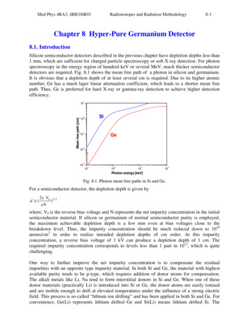
Med Phys 4RA3, 4RB3/6R03Radioisotopes and Radiation Methodology8-1Chapter 8 Hyper-Pure Germanium Detector8.1. IntroductionSilicon semiconductor detectors described in the previous chapter have depletion depths less than1 mm, which are sufficient for charged particle spectroscopy or soft X-ray detection. For photonspectroscopy in the energy region of hundred keV or several MeV, much thicker semiconductordetectors are required. Fig. 8.1 shows the mean free path of a photon in silicon and germanium.It is obvious that a depletion depth of at least several cm is required. Due to its higher atomicnumber, Ge has a much lager linear attenuation coefficient, which leads to a shorter mean freepath. Thus, Ge is preferred for hard X-ray or gamma-ray detection to achieve higher detectionefficiency.1Mean free path [cm]10Si010-110Ge-210-310110210310410Photon energy [keV]Fig. 8.1. Photon mean free paths in Si and Ge.For a semiconductor detector, the depletion depth is given byd (2 V0eN)1 / 2where, V0 is the reverse bias voltage and N represents the net impurity concentration in the initialsemiconductor material. If silicon or germanium of normal semiconductor purity is employed,the maximum achievable depletion depth is a few mm even at bias voltages close to thebreakdown level. Thus, the impurity concentration should be much reduced down to 1010atoms/cm3 in order to realize intended depletion depths of cm order. At this impurityconcentration, a reverse bias voltage of 1 kV can produce a depletion depth of 1 cm. Therequired impurity concentration corresponds to levels less than 1 part in 1012, which is quitechallenging.One way to further improve the net impurity concentration is to compensate the residualimpurities with an opposite type impurity material. In both Si and Ge, the material with highestavailable purity tends to be p-type, which requires addition of donor atoms for compensation.The alkali metals like Li, Na tend to form interstitial donors in Si and Ge. When one of thesedonor materials (practically Li) is introduced into Si or Ge, the donor atoms are easily ionizedand are mobile enough to drift at elevated temperatures under the influence of a strong electricfield. This process is so-called “lithium ion drifting” and has been applied in both Si and Ge. Forconvenience, Ge(Li) represents lithium drifted Ge and Si(Li) means lithium drifted Si. The
Med Phys 4RA3, 4RB3/6R03Radioisotopes and Radiation Methodology8-2lithium mobility is much greater in germanium and remains high enough at room temperature,which leads to an undesirable redistribution of the lithium. Therefore, the lithium profile ofGe(Li) detectors must always be preserved at LN2 temperature while Si(Li) detectors can bestored at room temperature for a short period due to low mobility of the Li ion in silicon.The other way to improve the net impurity concentration is to add additional refining processesso that the intended purity of the crystal can be met. Techniques have been developed to achievehigh purity Ge crystals in this approach and HyperPure Ge (HPGe) detectors are commerciallyavailable. However, no equivalent technique is available for Si yet.Ge(Li) detectors were popular in the past and served as the common type of large-volumegermanium detector for a long time. Although there is little difference in detector performancebetween HPGe and Ge(Li), the maintenance of Ge(Li) is pretty inconvenient, which has mademanufacturers stop producing them.8.2. ConfigurationsA. Hyper-Pure Germanium (HPGe) detector fabrication [4]HPGe crystal were first developed in the mid 1970s. The starting material is bulk germaniumintended for the semiconductor industry. Although already of very high purity, the material isfurther purified with the zone refining technique. The germanium is melted in a crucible usingradio-frequency (RF) heating coils. The underlying principle is that impurities concentrate in theliquid phase leaving the solid purer than the original melt as a liquid freezes and solid appears.Fig. 8.2. Three coil zone refine.Fig. 8.3. Growing Ge crystal.As shown in Fig. 8.2, each zone refiner coil melts a small section of the germanium in thecrucible. As the RF coils are slowly moved along the length of the crucible, the molten zonemoves with them. Thus, the germanium melts as the coil approaches and freezes as the coilmoves away. The impurities tend to remain in the molten section, which leads to a higherconcentration of impurities in the liquid than the solid. In this way, the impurities are swept toone end. This sweeping operation is repeated many times, until the impurities are concentrated atone end of the ingot. This end is then removed, leaving the remaining portion much purer than
Med Phys 4RA3, 4RB3/6R03Radioisotopes and Radiation Methodology8-3the original starting material. The improvement or reduction in impurity concentration actuallyrealized is about a factor of 100 or more at the completion of this process.Large single crystals of germanium are grown using the Czochralski technique. A precisely cutseed crystal is dipped into the molten germanium and then withdrawn slowly, while maintainingthe temperature of the melt just above the freezing point as shown in Fig. 8.3. The rate of crystalwithdrawal and temperature of the melt are adjusted to control the growth of the crystal. If theremaining extremely low-level impurities are acceptors, the property of the crystal is mildly ptype while high purity n-type is the result in the other case.B. Planar configurationAn example of a planar HPGe detector using a p-type crystal is shown in Fig. 8.4. In thisconfiguration, the electric contacts are provided on the two flat surfaces of a germanium crystal.Photons0.25 mm thick Bep (0.3 m B)ep-typehp-n junctionn contact (0.7 mm Li)Fig. 8.4. Planar HPGe detector (p-type).A lithium evaporation and diffusion to form the n contact is performed over one of the surface.This lithium-diffused layer is about several hundred µm thick. The depletion region is formed byreverse biasing n -p junction. The surface of the opposite side is modified to the p layer by ionimplantation of boron acceptor atoms to increase the conductivity near the surface. Since bothmaterials are p-type, no semiconductor junction exists at this side. Instead, the p layer providesthe electric contact to collect the charge carriers created by the radiation. The thickness of theimplanted boron layer is so thin (a few tenths of µm) that it is a suitable entrance window for lowenergy photons.To make a reverse bias, a positive high voltage is applied to the n contact with respect to the p surface. The depletion region is formed at the region close to the n contact and then expandeddeeply into the p-side as the bias voltage is raised. Once the detector is fully depleted, furtherincrease of the bias (overvoltage) does not make any effect on the sensitive volume, however, itmakes the electric field stronger, which subsequently shortens carrier collection times andreduces the risk of carrier losses (recombination and trapping).
Med Phys 4RA3, 4RB3/6R03Radioisotopes and Radiation Methodology8-4Planar HPGe detectors can also be fabricated starting with high-purity n-type crystals. Similarly,n and p contacts are provided on both sides. Reverse biasing also requires the application of apositive voltage to the n side. In this case, the depletion region is expanded from the p contact.When fully depleted and operated with a sufficient overvoltage, the electric field inside thecrystal is almost uniform and charge carriers drift under a constant electric field.C. Coaxial configurationFrom the photon mean free path in germanium, a detector thickness of the order of 5 cm isrequired for efficient detection of MeV photons. The maximum depletion depth for the planardetectors is limited to less than 1 or 2 cm. To produce a detector with a thicker depletion depth, adifferent electrode configuration must be employed. HPGe detectors dedicated for MeV photonsare constructed in coaxial geometry as shown Fig. 8.5. In this configuration, one electrode isfabricated at the outer surface of a cylindrical crystal and the other electrode is located at theinner surface of the central hole. In this way, much larger active volumes can be achieved.True coaxialClosed-ended coaxialFig. 8.5. Large volume coaxial HPGe detectors.A closed-ended configuration is one in which only part of the central core is removed and theouter electrode is extended over one flat side surface. This configuration is the most commontype of commercial HPGe detector.depletedp-n junctionp-n junctionFig. 8.6. Extension of the depletion region for a coaxial detector.
Med Phys 4RA3, 4RB3/6R03Radioisotopes and Radiation Methodology8-5In principle, the p-n junction of a coaxial detector can be located either at the inner or outersurface of the crystal as shown in Fig. 8.6. If the junction is on the outer surface, the depletionregion extends inward as the high voltage bias is increased until the crystal is fully depleted. Inthe opposite case, the depletion region grows outward. The p-n junction at the outer surfacerequires a much lower full depletion bias and therefore, is preferred.The practical electrode configurations of coaxial Ge detectors are shown in Fig. 8.7. To make thep-n junction at the outer surface, the n contact is performed over the outer surface for a p-typedetector while the p contact is applied in case of an n-type crystal. The n-type coaxial detectorsare often called reverse electrode detectors. The reverse bias requires a positive outsidepotential for a p-type and a negative potential for an n-type relative to the central electricpotential.p-typen-typep n n contactp contactFig. 8.7. Electrode configurations for coaxial detectors.Regardless of the crystal type, a coaxial detector can be used for general gamma-rayspectroscopy purposes. For low energy gamma-rays below 100 keV, a significant portion of theincident photons is attenuated for p-type detectors due to the relatively thick surface dead layer,i.e. lithium n contact. Thus, p-type coaxial detectors are normally limited down to 50 keV. Sincethe dead layer thickness of n-type detectors is much thinner, n-type detectors are still effectivefor low energy photons (down to several keV) when coupled to a thin Be entrance window.Therefore, n-type detectors cover quite a wide spectral region compared to p-type coaxial andplaner detectors.D. Electric field and capacitanceThe electric field in HPGe detectors governs the charge carrier collection process. The signalpulse shape and the timing behavior are consequently dependent on the variation of the electricfield strength. As discussed in the general properties of semiconductor detectors, the governingequation is Poisson’s equation: 2V The charge density is given as -eNA for p-type crystals and as eND for n-type crystals.For convenience, p-type crystals are assumed in the following derivation.
Med Phys 4RA3, 4RB3/6R03Radioisotopes and Radiation Methodology8-6Planar detectorsFrom the solution derived in the semiconductor detector chapter, the depletion depthcorresponding to a reverse bias V0 is2 V0 1 / 22 V0 1 / 2d (eN) (eN A)where, N represents the impurity concentration in the initial semiconductor material. If thecrystal thickness is T, the high voltage bias corresponding to the depletion depth T isVd eN A T 22 In this case, the detector is fully depleted and Vd is defined as the depletion voltage.In one-dimensional slab geometry as shown in Fig. 8.8, Poisson’s equation becomesT eN Ad V ( x) 2 dx2(0 x d)n p-typep For a partially depleted voltage, the equation is valid for the depletedregion. The boundary condition of the electric potential becomesV ( x 0) V ( x d ) V0x 0where x 0 represents the n contact position. The electric field isobtained by integrating the Poisson’s equation:V0 eN A d ( x) 2dFor a given bias voltage (if V0 Vd), this solutionis limited in the depleted region and the electricfield outside the depleted region is zero. Thevariation of the electric field strength for a planarHPGe detector is shown in Fig. 8.9. The depletionvoltage for NA 1010 cm-3 and T 1 cm is 565 V.The capacitance per unit area isC d ( 2V0Fig. 8.8. Partial depletionof a planar detector.(0 x d)1500101000V1000400V565V500100V)1 / 2for partial depletion conditions. Once the bias V0exceeds Vd, the detector capacitance becomesconstant and independent of the bias voltage.-3NA 10 cm , T 1 cmE(x) [V/cm]E ( x) x d200V00.00.20.40.60.81.0X [cm]Fig. 8.9. Electric field variation of a planar detector.
Med Phys 4RA3, 4RB3/6R03Radioisotopes and Radiation Methodology8-7Coaxial detectorsFor the true coaxial geometry, Poisson’s equationbecomesd 2V 1 dV eN A 2r dr dr40003000 VFor partial depletion conditions, solving for thedepletion depth is a little complicated, so that thebias voltage is assumed to be larger than thedepletion voltage. Then the boundary conditioncan be set asE(x) [V/cm]30002000 V2000Vd 1556 V10001000.0V (r2 ) V (r1 ) V0-3NA 10 cm , r1 4 mm, r2 2.5 cm0.51.0r [cm]1.52.02.5Fig. 8.10. Electric field variation of a true coaxialdetector.where r1 and r2 represent inner and outer radii. The electric field can be set as E (r ) rˆE (r )and is solved asV0 (eN A / 4 )(r22 r12 )V0 (eN A / 4 )(r22 r12 )eN AeN A E (r ) E (r ) r r 2 r ln(r2 / r1 )2 r ln(r2 / r1 )The depletion voltage Vd can be calculated from the conditionE (r1 ) 0 Vd eN A r22 r12 r12 ln(r2 / r1 ) 2 2 Fig. 8.10 shows the variation of the electric field for a true coaxial HPGe detector.The capacitance per unit length of a fully depleted true coaxial detector isC 2 ln(r2 / r1 )To make the capacitance as low as possible, the radius of the center core r1 is kept to a minimum.For the closed-ended coaxial detectors, thePoisson’s equation is hard to solveanalytically and therefore a numericalmethod like the Finite Difference Methodmust be employed. An example of thepotential variation and the electric fielddirection is shown in Fig. 8.11.Fig. 8.11. Potential and electric field distribution of aclosed-ended coaxial detector [5].
Med Phys 4RA3, 4RB3/6R03Radioisotopes and Radiation Methodology8-88.3. Operational characteristicsA. Cryostat and dewarAlthough silicon detectors can be operated at room temperature in principle, operatinggermanium detectors at room temperature is impossible due to the small bandgap energy, whichgenerates an intolerable leakage current. Therefore, germanium crystals must be cooled to reducethe leakage current. HPGe detectors are allowed to warm to room temperature when they are notin operation, however, they are always maintained at LN2 temperature practically.Fig. 8.12. Modern arrangement of HPGe detector and preamp within the cryostat housing.The Ge crystal is encased in a vacuum tight container (cryostat) to reduce thermal conductionbetween the crystal and the air. The basic function of a cryostat is to cool the germanium detectorto LN2 temperature. The germanium detector preamp is normally included as part of the cryostatpackage. Since the preamp should be located as close as possible so that the overall capacitancecan be minimized, the preamp is installed together. The input stages of the preamp are alsocooled. The entire cold assembly is maintained by the cryostat under high vacuum for boththermal insulation and protection of the internal components from contamination.
Med Phys 4RA3, 4RB3/6R03Radioisotopes and Radiation Methodology8-9All of the cryostat materials around the detector should be as low Z as possible to reduce photonscatter. Hence, aluminum, magnesium, beryllium, Teflon, and Mylar are used whenever possible.There are various types of dewars so that the detection geometry can be selected depending onthe application. For general radioactive or neutron-activated samples, the vertical type is widelyused. For in-beam spectroscopic purposes, either the horizontal or side-looking type is moreconvenient. Portable dewars are also available for outside field measurements.VerticalHorizontalSide-lookingFig. 8.13. Various configurations of LN2 dewars and cryostats.B. Energy resolutionThe most important characteristic of HPGe detectors is their excellent energy resolution. In Fig.8.14, two spectra from an HPGe and a NaI(Tl) are compared for a 60Co source. The greatsuperiority of the HPGe detector allows the separation of many closely spaced gamma lines,which is very beneficial for measuring multi-gamma emitting radioactive sources.25x10NaI (75 keV FWHM)HPGe (2.35 keV FWHM)2Counts/channel4x101173 keV23x101332 keV22x1021x1000500100015002000Photon energy [keV]Fig. 8.14. Comparison of NaI(Tl) and HPGe spectra for 60Co.
Med Phys 4RA3, 4RB3/6R03Radioisotopes and Radiation Methodology8-10The energy resolution of the HPGe photon spectroscopy system is governed by the variation inthe number of charge carriers, variation in the charge carrier collection, and the contribution ofelectronic noise. Hence, the FWHM of a peak in the spectrum can be represented asWT2 WD2 W X2 WE2where W values on the right-hand side are peak widths expected due to carrier statistics, carriercollection and electronic noise.The variation in the number of the charge carriers is given byE 2WDF NF 2.355 2.355 WD2 (2.355) 2 F (2.355) 2 FwE E NNNwhere E is the photon energy, N is the number of e-h pairs, F is the Fano factor, and w is theenergy required for creating a electron-hole pair. If the Fano factor is assumed to be 0.1, theequation predicts the WD value of 1.3 keV at 1.33 MeV when the w value of 3 eV is used.The contribution of the second term is due to incomplete charge collection and becomesimportant for large volume or low electric field detectors.The last term represents the broadeningeffects of all electronics following thedetector. This component can be measuredwith a precision pulser as discussed in thepulse processing chapter. The pulser output isfed to the test input of the preamp and itundergoes exactly the same path as that of theactual signal from the detector.Fig. 8.15 shows the contribution of eachcomponent as a function of the photonenergy. At low energies, electronic noise andcharge collection are relatively importantwhile the additional broadening due to carrierstatistics becomes significant at higherenergies.Fig. 8.15. Dependence of resolution on photon energy.C. Pulse shape and timing propertiesThe detailed shape of the signal pulse is important for determining the shaping time of the pulseheight spectroscopy and for applications requiring timing information. The ultimate timeresolution obtainable from HPGe detectors depends on both the average rise time and thevariation in the pulse shape from event to event.Two factors limit the ultimate time resolution of HPGe detectors. The first factor is the slowprocess of the charge carrier collection. If the electric field is strong enough, the drift velocitiesof electron and hole are saturated. The electron saturation drift velocity is 105 m/s, which
Med Phys 4RA3, 4RB3/6R03Radioisotopes and Radiation Methodology8-11makes a travel time of 100 ns/cm. Typical pulse rise times will be of this order and are muchlonger than those of organic scintillation detectors. The second factor is the large variation in theshape of the output pulses. The leading edge of the pulse changes substantially from event toevent depending on the position of electron-hole creation.The pulse shape of planar detectors can be described from the energy balance as follows.The infinitesimal induced charge is given bydW V0 dQwhere, dW is the work done on the charge carriers, V0 is the applied voltage and dQ is theinduced charge. The work done on the charge carriers with charge q0 isdW q0 dV ( x) VdW q 0 E ( x) q0 0dxTwhere, E(x) is the electric field and T is the detector thickness. The energy absorbed by themotion from x0 to x isx W dW x0q0V0 xq 0V0( x x0 ) dx TT x0which induces charge Q as Q dQ x x0vt W q0 q0V0TTThe corresponding signal voltage VR can be represented as V R Q q 0 vt CC TThere are two components of the induced charge: one from the motion of electrons, the otherfrom holes. Let’s suppose charge carriers were produced at a distance x from the n layer after aphoton interaction as shown in Fig. 8.16.In the initial stage of the charge carrier collection, both electrons and holes are drifting, thus,Q(t ) q0 (vevt h t)TTIf electrons have been collected, but holes are still drifting,Q (t ) q 0 (le vh t)T ThxeIn the opposite case (holes have been collected),Q (t ) q0 (veT let )TTAfter both holes and electrons are collectedQ(t ) q0Fig. 8.16 shows typical patterns of pulse shapes depending on the production positions of e-hpairs.
Med Phys 4RA3, 4RB3/6R03Radioisotopes and Radiation Methodology8-12Fig. 8.16. Shape of the leading edge of the output pulse Q(t) for a planar HPGe detector.8.4. Photon spectroscopy with HPGe detectorsA. Detector response [6]Fig. 8.17. Pulse height spectrum of 54Mn single gamma emitter.The response of a HPGe detector for a single gamma emitter is shown in Fig. 8.17. Interactionevents contributing the full-energy peak are more likely to consist of multiple interactions, suchas Compton scattering followed by photoelectric absorption of the scattered photon. Absorptionof the full photon energy in a single photoelectric effect is pretty rare. The table belowsummarizes a Monte Carlo simulation result.Number of interactions contributing to the 1332 keV peak for a coaxial HPGe detector1234564.2 %17.8 %27.0 %25.1 %15.4 %7.0 %
Med Phys 4RA3, 4RB3/6R03Radioisotopes and Radiation Methodology8-13As the photon energy increases above 2mec2, the pair production interaction becomes dominantand the escape peaks are quite important. The spectra in Fig. 8.18 show different patterns of thefull-energy, single escape, double escape peaks depending on the photon energy.Fig. 8.18. The relative intensity of the full-energy, single escape and double escape peaksfor a coaxial detector.Fig. 8.19. Pulse height spectrum of a HPGe detector for 56Mnmulti-gamma emitter.
Med Phys 4RA3, 4RB3/6R03Radioisotopes and Radiation Methodology8-14Fig. 8.19 is an example of the response for a multi-gamma emitter. Thanks to the excellentresolution, each peak is well identified, which is pretty important for analyzing a complicatedspectrum.B. Compton suppression systemGeGeFig. 8.20. Guard detector arrangements for Compton suppression.The Compton continuum in photon spectra from HPGe detectors is generated primarily byphotons that undergo one or more scatterings in the detector followed by escape of the scatteredphoton from the active volume. If those events contributing to the continuum are rejected, thepeak-to-continuum ratio is greatly improved and accordingly, the minimum detectableradioactivity can be reduced significantly. To realize a rejection process, the HPGe detector issurrounded with a Guard detector (inorganic scintillation type) as shown in Fig. 8.20. Then thepulse processing system can reject the escape events by the anticoincidence technique whenproper timing electronics are implemented. In other words, the pulse processing system acceptseach detection event from the HPGe only when there is no detection event from the guarddetector in coincidence. Figs. 8.21 and 8.22 show a standard pulse processing system forCompton suppression and an example of the suppression effect.Fig. 8.21. Standard pulse processing system for Compton suppression.
Med Phys 4RA3, 4RB3/6R03Radioisotopes and Radiation Methodology8-15Fig. 8.22. 137Cs spectrum with and without the Compton suppression.C. Efficiency calibrationConventionally, the relative efficiency is conveniently used for quoting the peak efficiency of aHPGe detector. The relative efficiency is defined asRel. eff. HPGe peak effi/NaI(Tl) (3 3 ) peak effiat 1332 keV from 60Co. The source-detector distance of 25 cm is uniquely used for this definition.The absolute peak efficiency of a 3 3 NaI(Tl) is 1.2 10-3 in this geometry.A typical variation of the full-energy peak efficiencies for coaxial detectors is shown in Fig. 8.23.Due to the relatively thick dead layer, the p-type efficiency starts dropping at 100 keV whilethe n-type efficiency is constant down to 5 keV.Fig. 8.23. Absolute efficiencies of n-type and p-type coaxial detectors.
Med Phys 4RA3, 4RB3/6R03Radioisotopes and Radiation Methodology8-16A practical example of the efficiency calibration for a wide dynamic range is shown in Fig. 8.24.The experimental efficiency data points were obtained from standard calibration sources up to 1.5 MeV and extended up to 12 MeV with both 14N(n, ) and 35Cl(n, ) prompt gamma-rays. Themeasured data points are converted into the log E versus the log of the efficiency and then fittedwith a polynomial so that a wide energy region is covered.Fig. 8.24. Fitting of a HPGe detector efficiency in a wide energy region.8.5. Medical applicationsA. In vivo X-ray spectrometry [7,8]In our department, planar HPGe and Si(Li) detectors have been used for in vivo X-rayspectrometry to analyze both trace (Pb, Hg, As etc.) and major (Sr) elements in the bodyquantitatively. The targeted elements are excited either with radiation from a radionuclide or anX-ray generator and then the characteristic X-rays are emitted and detected. Fig. 8.25 shows asystem developed for Hg and an example phantom spectrum.Fig. 8.25. In vivo X-ray spectrometry system for measuring mercury and a phantom spectrum [8].
Med Phys 4RA3, 4RB3/6R03Radioisotopes and Radiation Methodology8-17B. Collimator-less Compton imaging(a)(b)Fig. 8.26. Concept of collimator-less Compton imaging (a) and three projected cones intersecting at onepoint (b) [9,10].Segmented (or position sensitive) semiconductor detector technology has been developingrapidly. For medical applications, this class of semiconductor detector makes possiblecollimator-less gamma-ray imaging. In principle, Compton imaging is effective even with asingle segmented detector if the scattering process inside the detector can be tracked (gammaray tracking [11]) with sufficient spatial resolution. With a highly segmented structure of Ge orSi, accurate information on both interaction position and deposited energy can be analyzed. Fromthis information, the interaction sequence of the photon inside the detector can be extracted witha proper tracking algorithm using the Compton scattering formula studied in the chapter 5. Then,the direction cone of the incident photon is obtained. Since the segmentation of the electrode isphysically limited, the pulse shape analysis technique is employed to further improve the spatialresolution. Finally, the source position is constructed as shown in Fig. 8.26. Both planar andcoaxial configurations have been developed.Fig. 8.27. Two-dimensionally segmented closed-ended coaxial (40-fold) and planar detectors (2 39-fold).
Med Phys 4RA3, 4RB3/6R03Radioisotopes and Radiation Methodology8-18References1. G.F. Knoll, Radiation Detection and Measurement - 3rd edition (Chapters 12 and 13), John Wiley &Sons, 1999.2. G. Gilmore, J.D. Hemingway, Practical Gamma-Ray Spectrometry, John Wiley & Sons, 1995.3. K. Debertin, R.G. Helmer, Gamma- and X-ray Spectrometry with Semiconductor Detectors, NorthHolland, 1988.4. HPGe Detector Manufacturing, ORTEC, URL: http://www.ortec-online.com/.5. Th. Kröll et al., Nucl. Intstr. and Meth. A 371 (1996) 489.6. Online Ge(Li)-Si(Li) Gamma Spectrum Catalog, Gamma-ray Spectrometry Center, Idaho NationalLaboratory, Published 3-29-1999, URL: http://www.inl.gov/gammaray/catalogs/.7. D.R. Chettle, X-Ray Spectrom. 34 (2005) 446.8. J. Grinyer, M. Popovic, D.R. Chettle, X-Ray Spectrom. 36 (2007) 99.9. L. Mihailescu et al., Nucl. Intstr. and Meth. A 570 (2007) 89.10. K. Vetter, M. Burks, L. Mihailescu, Nucl. Intstr. and Meth. A 525 (2004) 322.11. I.Y. Lee, Nucl. Intstr. and Meth. A 422 (1999) 195.
Med Phys 4RA3, 4RB3/6R03Radioisotopes and Radiation Methodology8-19Problems1. For a 2 cm thick planar HPGe detector given below:(a) In order to use as a radiation detector, which surface must be keptat zero voltage and which surface must be kept at a high voltage ?Which polarity of a high voltage must be applied ? Briefly explainthe reason.p 2 cm0.5 cmAp-typen (b) The E-field distribution for V0 200 V is shown. Find thedepletion voltage.(c) Suppose a gamma interaction happened at the position A. Sketchthe expected signal shape, i.e. Vout(t) as a function of time t. Indicatethe contribution by holes and the contribution by electrons. Brieflyexplain the reason.E(x) [V/cm]100050000.0 0.2 0.4 0.6 0.8 1.0 1.2 1.4 1.6 1.8 2.0X [cm]2. An n-type HPGe coaxial detector has the following geometry:(a) To which surface, a p-type impurity must be added ? Briefly explain the reason.(b) Sketch equipotential lines for a full depletion condition.(c) Sketch the drift direction of electrons and holes created at the position A. Do thesame work for the position B.3. Suppose you aim to measure an unknown photon radiation field in the energy range of 20 keV to 5MeV using a semiconductor detector. Write down i) a proper detector material, ii) type and iii)configuration. Briefly justify the reason.4. For a p-type true coaxial HPGe detector, the electric field for an applied bias voltage V0 at the fulldepletion condition is given by eN AV ( eN A / 4 )( r22 r12 )E ( r ) rˆE ( r ) , E ( r ) r 02 r ln( r2 / r1 )Find the depletion voltage.5. A p-type planar HPGe detector has a depletion voltage of 1,500 V.(a) Sketch the electric field E(x) as a function of the depth x for three bias voltages 500, 1,000 and 2,000V. For convenience, x 0 is located on the n surface.(b) For the partial depletion condition, explain how the depletion depth changes as you increase the biasvoltage.
Med Phys 4RA3, 4RB3/6R03Radi
Ge(Li) detectors were popular in the past and served as the common type of large-volume germanium detector for a long time. Although there is little difference in detector performance between HPGe and Ge(Li), the maintenance of Ge(Li) is pretty inconvenient, which has made manufacturers stop producing them. 8.2. Configurations