Transcription
Computers and Chemical Engineering 113 (2018) 184–195Contents lists available at ScienceDirectComputers and Chemical Engineeringjournal homepage: www.elsevier.com/locate/compchemengMultiscale three-dimensional CFD modeling for PECVD of amorphoussilicon thin filmsMarquis Crose a, Weiqi Zhang a, Anh Tran a, Panagiotis D. Christofides a,b, abDepartment of Chemical and Biomolecular Engineering, University of California, Los Angeles, CA 90095, USADepartment of Electrical and Computer Engineering, University of California, Los Angeles, CA 90095, USAa r t i c l ei n f oArticle history:Received 20 January 2018Revised 7 March 2018Accepted 14 March 2018Available online 17 March 2018Keywords:Multiscale modelingComputational fluid dynamicsThin film growthParallel computinga b s t r a c tThe development of a three-dimensional, multiscale computational fluid dynamics (CFD) model is presented here which aims to capture the deposition of amorphous silicon thin films via plasma-enhancedchemical vapor deposition (PECVD). The macroscopic reactor scale and the microscopic thin film growthdomains which define the multiscale model are linked using a dynamic boundary which is updated atthe completion of each time step. A novel parallel processing scheme built around a message passinginterface (MPI) structure, in conjunction with a distributed collection of kinetic Monte Carlo algorithms,is applied in order to allow for transient simulations to be conducted using a mesh with greater than 1.5million cells. Due to the frequent issue of thickness non-uniformity in thin film production, an improvedPECVD reactor design is proposed. The resulting geometry is shown to reduce the product offset from 25 nm to less than 13 nm using identical deposition parameters. 2018 Elsevier Ltd. All rights reserved.1. IntroductionThe past two decades have seen continual development in themultiscale modeling of plasma-enhanced chemical vapor deposition (PECVD) with specific applications to the manufacturing ofsilicon thin films for use in the photovoltaic and microelectronics industries (e.g., Collins et al. (1994); da Silva and Morimoto(2002); Rasoulian and Ricardez-Sandoval (2015)). Accurate modeling of thin film deposition remains a key element in the effort toimprove product quality and to cut down on manufacturing costsdue to the difficulties associated with continuous and/or in situmeasurements during chambered deposition processes (Economouet al., 1989; Rasoulian and Ricardez-Sandoval, 2014; 2015). Recently, Crose et al. (2017b) demonstrated a novel multiscale computational fluid dynamics (CFD) model, which combined a macroscopic CFD domain with a microscopic surface domain through acommon boundary which lies on the surface of the silicon wafer.Although advanced modeling of chemical reactors via CFD has existed for some time (Gerogiorgis and Ydstie, 2005), the work ofCrose et al. (2015) was the first to capture the link between PECVDreactor behavior and the microscopic domain. In particular, nonuniform deposition of a-Si:H (amorphous silicon) films was stud- Corresponding author at: Department of Chemical and Biomolecular Engineering, University of California, Los Angeles, CA 90095, USAE-mail address: pdc@seas.ucla.edu (P.D. ng.2018.03.0110098-1354/ 2018 Elsevier Ltd. All rights reserved.ied and provided a basis for future multiscale CFD modeling endeavors. Nonetheless, the two-dimensional axisymmetric nature ofthe model limits the exploration of some phenomena which exist in the three-dimensional in space process. Specifically, twodimensional (2D) axisymmetric models cannot represent the fullgeometry of showerhead holes that provide reactant gases to theplasma region – a key feature when considering the uniformity ofthin film products.Given the aforementioned motivations, the framework previously developed for use in 2D applications is extended here tothe three dimensional in space domain. Using a three-dimensional(3D) rendering which captures the typical geometry of chambered, parallel-plate PECVD reactors, a CFD model is proposed inthe present work which is capable of reproducing accurately bothplasma chemistry and fluid flow into the reaction zone through theshowerhead region. With regard to the microscopic domain (i.e.,the surface of the silicon wafer), a detailed kinetic Monte Carlo(kMC) algorithm developed previously by Crose et al. (2017b) isapplied in order to capture both the exchange of mass and energy, as well as the microstructure of the a-Si:H thin film. Giventhat the startup and operation of PECVD reactors are inherentlydynamic, the proposed simulations cannot derive accurate reactor behavior from steady-state solutions; however, the computationally demanding nature of the transient simulations necessitatesthe use of a parallel computation strategy as well as taking advantage of multiple-time-scale phenomena occurring in the process. In this work, a Message Passing Interface (MPI) structure is
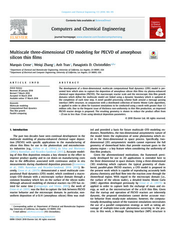
M. Crose et al. / Computers and Chemical Engineering 113 (2018) 184–195185Given the primary motivation of addressing a-Si:H thin film product quality (in particular, thin film spatial non-uniformity) throughimproved PECVD reactor design, in this work the development ofa 3D multiscale CFD model will be presented including both themacroscopic and microscopic domains, as well as the associateddynamic boundary conditions and parallel computing implementation.2.1. CFD geometry and meshingFig. 1. (a) 2D axisymmetric geometry after discretization using a structured meshcontaining 120,0 0 0 cells. (b) Collection of 1.5 million polygons which define theunstructured, 3D mesh.adopted which allows for the discretization of both the macroscopic CFD volume and the microscopic kMC algorithm. The outlined multiscale model including its parallel implementation is applied to the deposition of 300 nm thick a-Si:H thin films revealing significant non-uniformities in the thickness of the thin filmproduct. An improved reactor geometry is proposed which utilizesa polar showerhead arrangement and a radially-adjusted showerhead hole diameter. This geometry is shown to reduce thicknessnon-uniformity in the a-Si:H thin film product from 8% to lessthan 4%, representing significant product quality improvement andfinancial savings.2. Three-dimensional modelingRecently, Crose et al. (2017b) demonstrated the need for multiscale modeling in the PECVD process due to the interconnection between the macroscopic, reactor scale and the microscopic,thin film growth domains. Specifically, a two-dimensional (2D) axisymmetric geometry was used in the creation of the reactor meshand a hybrid kinetic Monte Carlo (kMC) algorithm was applied tocapture the growth of amorphous silicon (a-Si:H) thin film layers.The common boundary between the reactor mesh and microscopicmodel is of key importance as it allows for the distinct domains toremain linked throughout the course of transient simulations, andwill be discussed at length in the multiscale workflow section. Although this model has proved useful in designing optimized reactor operational strategies, some features of the PECVD reactor arelost when using 2D representations. In looking at Fig. 1a and 1 b,the difference between showerhead geometries becomes clear: thecylindrical showerhead holes and their associated spatial arrangement of the 3D system cannot be directly translated to 2D models.As discussed previously, we utilize a 3D, cylindrical PECVD reactor geometry (see Fig. 1b) with dimensions typical of those used inindustry. The showerhead holes, visible in Figs. 1b and 14 a, havea diameter of 1 cm and are evenly spaced in a rectangular arraythroughout the inlet region. In order to solve the partial differential equations which capture the gas phase mass, momentum andenergy balances, the reactor geometry is discretized using an unstructured mesh containing 1.5 million tetrahedral cells. Whileprevious efforts in modeling PECVD systems have relied on structured meshing (e.g., Crose et al. (2017b)) due to the possibility forhigher mesh quality, in terms of orthogonality and aspect ratio,these models were based on 2D geometries with rectangular structures; however, in this work the curvature of the cylindrical reactor shell and showerhead holes favor the use of unstructured meshcompositions.Specifically, the reactor mesh is built from a collection of tetrahedral cells with non-uniform cell density. Regions in which significant gradients are expected in temperature, species concentration,flow velocity, etc. (i.e., near walls, corners and highly curved surfaces) have been given higher cell density as opposed to the bulkfluid regions, see Fig. 1b. In order to obtain industrially relevantplasma distributions and thin film growth, accurate flow modelingof the process gas throughout the chamber is paramount. As an additional consideration, the cell density near surfaces is directly correlated to the flow characteristics of the gas, and in particular, theboundary layer which is formed at the interface of the fluid andsolid phases. Given the relatively low flow rate of process gas (75SCCM) and low chamber pressure (1 Torr), flow along the surfaceof the wafer is expected to be laminar (note: preliminary resultsfrom the macroscopic model and earlier work suggest a Reynold’snumber of Re 2.28 10 4 ). As a result, the mesh density directly above the substrate surface has been tuned such that theboundary layer may be captured within one cell ‘layer’ to provideaccurate predictions necessary for the linked microscopic model.Although the choice to use an unstructured mesh in this mannerrather than a simplified structured mesh comes at the cost of computational efficiency, the ease in designing new reactor geometrieswithout constraints for showerhead hole size and curvature necessitates its use and the associated computational demands will bediscussed at length in the parallel programming section below.It is important to note that throughout this work ANSYS software is applied to the creation of the geometric mesh (specifically,ICEM meshing) and as a solver for the PDEs describing transportphenomena and chemical reactions (ANSYS Inc., 2013). The ANSYS Fluent software alone cannot yield a multiscale model for thePECVD process of interest; consequently, three user defined functions (UDFs) have been developed to tailor the solver to the deposition of a-Si:H thin films. More specifically, the thirty four mostdominant gas phase reactions have been accounted for via a volumetric reaction scheme which includes terms for the nine primary plasma reactions which lead to thin film growth. The necessary electron density within the plasma region is calculated using a product of the zero-order Bessel function and a sine functionwhich account for the spatial dependencies within the cylindricalreaction zone. The third UDF necessary to the multiscale natureof the model simulates the growth of a-Si:H thin films along the
186M. Crose et al. / Computers and Chemical Engineering 113 (2018) 184–195Table 1Reactions included in the gas-phase model. Note: Rate constants have units of cm3 /sand have been adopted from the collection prepared by Kushner (1988).Fig. 2. Individual unit cell within the unstructured mesh.surface of the wafer substrate. The details of these UDFs, in particular the kinetic Monte Carlo (kMC) algorithm which defines themicroscopic domain, are expanded upon at length in the followingsections.2.2. Gas-phase modelGrowth of amorphous silicon layers within a PECVD reactor isintimately tied to the physio-chemical phenomena that govern thegas phase. Mass, momentum and energy balances each play a keyrole in predicting the conditions at the shared boundary betweenthe macroscopic and microscopic domains. To that end, traditionalanalytic solutions to the gas-phase model are viable only for simplified geometries or systems which fail to provide meaningful results that can be applied to industrially used PECVD systems. Bydefining the mesh structure as described in the previous section,numerical methods may be introduced which are capable of solving the complex computational fluid dynamics equations with highresolution. Specifically, at every time step, the governing equationsare discretized in alignment with the cell distribution presented inFig. 1b, allowing for the ANSYS Fluent solver to implement finitevolume methods. Extended functionality of the Fluent solver (i.e., atailored solution specific to deposition via PECVD) is achieved using the aforementioned user defined functions (see Fig. 2 for anexample tetrahedral cell element as viewed by the solver).The continuity, energy and momentum equations employed inthis work are standard and as such will be presented only brieflywithout rigorous derivation. An in-depth description of the flowfield equations can be found in the Fluent user manual (ANSYS Inc.,2013). In a generalized vector form, the governing equations aregiven by the following system: (ρ v ) (ρ v v ) p τ̄ ρ g F t 2τ̄ μ ( v vT ) vI3(1)(2) (ρ E ) ( v(ρ E p)) (k T hJ (τ̄ v )) Sh t(3) (ρYi ) · (ρ vYi ) · Ji Ri Si t(4) Ji ρ Di,m Yi DT,i TT(5)where ρ is the density of the gas, v is the physical velocity vector,p is the static pressure, τ̄ and I are the stress and unit tensors,ReactionMechanismRate 4e H2 2He SiH4 SiH3 He SiH4 SiH3 He SiH4 SiH2 2He SiH4 SiH H2 He SiH4 Si H2 2He Si2 H6 SiH3 SiH2 He Si2 H6 H3 SiSiH 2He Si3 H8 H3 SiSiH SiH4H SiH2 SiH3H SiH2 SiH H2H SiH3 SiH2 H2H SiH4 SiH3 H2H H2 Si SiH2 Si2 H5H Si2 H6 SiH4 SiH3H Si2 H6 Si2 H5 H2H Si3 H8 Si2 H5 SiH4H2 SiH SiH3H2 SiH2 SiH4SiH2 SiH4 Si2 H6SiH3 SiH3 SiH4 SiH2SiH3 SiH3 Si2 H6SiH SiH4 Si2 H5SiH2 SiH4 H3 SiSiH H2SiH2 Si2 H6 Si3 H8SiH2 SiH3 Si2 H5SiH3 SiH3 SiH4 SiH2SiH3 Si2 H6 SiH4 Si2 H5Si2 H5 SiH4 SiH3 Si2 H6SiH3 Si2 H5 Si3 H8H3 SiSiH SiH4 Si3 H8Si2 H5 Si2 H5 Si3 H8 SiH2H3 SiSiH H2 Si SiH2H2 Si SiH2 H3 SiSiH7.66 10129.57 10133.40 10121.13 10135.62 10126.70 10122.15 10137.41 10133.35 10146.68 10111.20 10131.20 10131.38 10123.01 10124.03 10127.83 10121.19 10121.20 10121.20 10116.02 10124.22 10126.02 10121.51 10126.02 10127.23 10132.27 10114.06 10131.98 10133.01 10119.03 10136.02 10129.03 10132.71 10132.29 1010J is the diffusive flux, Yi is the mass fraction of species i, Di is thediffusion coefficient of species i, and Sh , Ri and Si are terms specificto the UDFs utilized in this work and will be defined below.As mentioned in the previous subsection, three predominantUDFs are used to tailor the functionality of the generalized Fluent solver to the problem of interest in this work, the first ofwhich accounts for the volumetric reactions occurring above thesubstrate surface. Although extensive reaction sets have been proposed which detail all possible intermediate and aggregate speciesinvolved in the deposition of a-Si:H films (e.g., Kushner (1988)),here we limit the scope to the twelve most dominant species andtheir associated thirty-four gas-phase reactions. A complete listing of the reactions, mechanisms and rate constants are given inTable 1. Thus, the Ri terms in the mass balance presented aboveare a product of this reaction set and are updated by the UDF during each time step.The terms Sh and Si appearing in Eqs. 3 and 4, respectively,refer to user defined sources or sinks. During the deposition ofamorphous silicon, mass is drawn from the gas phase in the formof SiH3 and H radicals, and mass is likewise reintroduced to themacroscopic domain due to hydrogen abstraction from the substrate surface via the formation of the stable species, SiH4 (note:this phenomena is visible in Fig. 4a). The Si term acts as a dynamic boundary condition which is updated based on the transfer of mass during the previous microscopic simulation cycle, withunits of kg s 1 m 2 . In other words, at the end of a time step theamount of mass (for each species) withdrawn from, or introducedto, the macroscopic domain is reported from the individual microscopic calculations. Subsequently, the boundary conditions forthe two-dimensional areas which define the interfaces of the kMCregions are updated before the next time step commences. Additionally, the formation and breaking of chemical bonds along the
M. Crose et al. / Computers and Chemical Engineering 113 (2018) 184–195187Fig. 3. Electron density within 3D axisymmetric PECVD geometry (cm 3 ).Fig. 4. (a) Finite element adjacent to the substrate surface with dynamic boundary condition calculated via microscopic simulation domain. (b) Kinetic Monte Carlo setupwithin overall multiscale simulation. Wafer substrate discretized in both the x and y directions forming a ‘grid’ structure.amorphous surface causes an exchange of energy between the substrate and the continuous gas phase which is tracked through theSh term. For clarification on the dynamic boundary conditions andtheir role in the overall multiscale model, please refer to the multiscale workflow section below.2.2.1. Electron density profileIn looking at Table 1, reactions R1 through R9 involve the interaction of free electrons and stable species; these nine reactionsdefine the plasma chemistry necessary for the deposition of SiH3and H. As such, the electron density is key to the accuracy of theplasma phase and the corresponding growth of thin film layers.For plasmas generated from radio frequency (RF) discharges withincylindrical geometries, literature has shown that the electron density can be accurately estimated from the product of the zero order Bessel function and a sine function whose period is twice thedistance between the showerhead and wafer substrate (Park andEconomou, 1991). This is described by the following equation: ne (r, z ) neo · J0 2.405rrt · sin πz D,(6)where neo is the maximum electron density, J0 is the zero orderBessel function of the first kind, rt is the radius of the reactor,and D is the distance between the showerhead and wafer (i.e., theparallel plate spacing). The distribution seen in Fig. 3 is the result of applying the aforementioned electron density to the threedimensional PECVD geometry presented earlier. The free electron‘cloud’ remains bounded by the charged region between the cylindrical walls of the reaction chamber and the parallel plates whichmake up the showerhead and substrate platform. As expected, thezero order Bessel function enforces a maximum density in the cen-ter of the reactor which trails off near the exit ports along theedge.2.3. Microscopic domainWhile the CFD model itself, along with the UDFs for the gasphase reactions and electron density, define the macroscopic domain, the microscopic domain is contained entirely within thethird and final UDF; specifically, as radicals diffuse from the gasphase down to the substrate surface, they enter the microscopicdomain. In looking at Fig. 4a, finite elements (i.e., mesh cells)which share a boundary with the substrate surface allow for theexchange of SiH3 and H radicals. This mechanism makes possiblethe interconnection between the two distinct simulation domains.While tracking of each individual particle remains a computationally infeasible task, growth of a-Si:H thin film layers may still beachieved using a network of parallel kinetic Monte Carlo (kMC) algorithms. Specifically, the substrate surface is broken down intodiscrete regions along the x y plane as shown in Fig. 4b, andwithin each region an independent kMC simulation is executed.Each simulation consists of a lattice of width 1200 particles whichcaptures the growth of a representative a-Si:H layer within theassociated region. The tetrahedral cells bordering each region areassigned dynamic boundary conditions corresponding to the exchange of mass and energy due to thin film growth at each timestep (see Fig. 4a). Details concerning the development of the microscopic UDF, including both the parallel kMC structure and dynamic boundary conditions, will be discussed in detail in the following subsections.
188M. Crose et al. / Computers and Chemical Engineering 113 (2018) 184–1952.3.1. Thin-film growth chemistryBefore the microscopic model is presented, it is importantto detail the chemical phenomena which occur along the surface of the growing thin film layer. Only SiH3 and H appear inthis text as deposition species due to experimental results fromPerrin et al. (1998) and Robertson (20 0 0) which indicate thatgreater than 98% of amorphous silicon deposition can be attributedto these species alone.In order for growth of the a-Si:H thin film to occur, particlesmust diffuse from the gas phase to the wafer substrate, and subsequently stick to the hydrogenated surface. Upon striking the surface, SiH3 and H radicals may either be deflected back into thegas phase or physisorption may occur at hydrogenated silicon sites( Si H) as evidenced by the following reaction set:The probability for a particle which strikes the surface to remainon the surface is known as the sticking coefficient and will be considered in the kinetic Monte Carlo section to follow. Once a weakhydrogen bond has been formed, physisorbed radicals may followone of two distinct mechanisms; the first and most dominant ofwhich is rapid diffusion across the surface of the lattice via migration:the range of 10–20%, our recent works have alternatively utilizeda triangular framework (Crose et al., 2017a,b). By eliminating therestriction of SOS behavior and introducing close-packed groupswith a minimum of two nearest neighbors, overhangs may developwhich in turn lead to voids in the triangular lattice (see Fig. 6). Itis important to note that while the overall multiscale model operates in three dimensional space, the lattice which defines themicroscopic domain remains two dimensional. Although the effortrequired to expand the lattice structure into a third coordinate isrelatively minimal, the computational cost of doing so would benon-trivial. Given that the goal of the microscopic model (i.e., thelattice structure and associated kinetic Monte Carlo algorithm), isto capture the growth rate of amorphous silicon deposition, nothing would be gained from a three dimensional lattice; particle interactions, void formation and steric hindrance are accurately expressed in the proposed triangular lattice model.Each grid location defined in Fig. 7 represents an independentmicroscopic simulation. Within these discrete grid cells exists arepresentative triangular lattice whose size can be characterized bythe product of the length and thickness. The number of lateral sitesis denoted by L and is proportional to the physical lattice length by0.25 L, given a hard-sphere silicon diameter of 0.25 nm. Thethickness, τ , may be calculated from the number of monolayers, H,by the following equation: Si H · · · SiH3 (s ) Si H Si H Si H · · · SiH3 (s ) Si H · · · H(s ) Si H Si H Si H · · · H(s ) .τ 0.25 · H ·SiH3 (g ) Si H Si H · · · SiH3 (s )H(g ) Si H Si H · · · H(s ) .(7)(8)Alternatively, a particle may return to the gas phase through theabstraction of a surface hydrogen, Si H · · · SiH3 (s ) Si H Si H Si0 SiH4 (g ) ,(9)whereby a physisorbed radical removes a neighboring hydrogenatom and reforms the stable species (e.g., SiH4 or H2 in the case oftwo species deposition). This process leaves behind dangling bonds( Si0 ) which are crucial to the growth of the amorphous siliconfilm. Growth of the lattice proceeds unit by unit via chemisorptionof SiH3 at dangling bond sites (i.e., the Si atom forms a covalentbond, permanently fixing its location within the amorphous structure) as shown in the following reactions: Si H · · · SiH3 (s ) Si0 Si H Si SiH3 Si0 SiH3 (g ) Si SiH3 .(10)The second reaction listed above suggests a gas phase radical maydirectly chemisorb at an existing dangling bond site without firstmigrating around the hydrogenated surface. While these events areunlikely due to the relative infrequency of dangling bonds acrossthe surface area of the a-Si:H film, they are not strictly forbiddenand must be considered in the development of the microscopicmodel. It is important to note that chemisorption of H only resultsin a return of the surface to its original, hydrogenated state: Si H · · · H(s ) Si0 Si H Si H Si0 H(g ) Si H .(11)A simplified illustration of the surface chemistry can be seen inFig. 5.2.3.2. Lattice characterization and relative ratesIn our early work on modeling PECVD systems (Crose et al.,2015), a solid-on-solid (SOS) lattice was used to represent themicroscopic structure of the growing a-Si:H thin film. Althougha two-dimensional SOS lattice remains the most efficient latticestructure from a computational standpoint, no vacancies or voidsare permitted within the bulk material. Given that experimentally grown a-Si:H layers are observed to have void fractions in 3,2(12)where the factor 0.25 accounts for the diameter of individual silicon atoms and 3/2 accounts for the reduction in thickness dueto the offset monolayers which result from the close-packed structure of the triangular lattice (refer to Fig. 6). The number of lateralsites remains fixed at L 1200 for each discrete microscopic simulation zone. This length allows for adequate development of thinfilm morphology and reduces wall effects without being so large asto necessitate the inclusion of spatial variations across individuallattices. To be clear, while significant gradients exist in the speciesconcentrations within the PECVD reactor and from one grid location to another (e.g., Figs. 4b and 7), finite microscopic simulationsof length 300 nm can be assumed to experience uniform deposition.Migration and hydrogen abstraction involve species which exist on the surface of the thin film; as a result, these reactions arethermally activated events and follow a standard Arrhenius-typeformulation:rt,i vi e Ei /kB T ,(13)(s 1 )where vi is the attempt frequency prefactorand Ei is the activation energy of radical i. Frequency prefactor and activation energy values are drawn from Bakos et al. (20 05, 20 06) to correspondto the growth of a-Si:H films via the two species deposition of SiH3and H.Physisorption events originate within the gas-phase and can bedescribed by an athermal or barrierless reaction model based onthe fundamental kinetic theory of gases which yields the followingrate equation:ra,i Ji sc Na σ ,(14)where J is the flux of gas-phase radicals, sc is the local sticking coefficient (i.e., the probability that a particle which strikes the surface will ‘stick’ rather than bouncing off), Na is the Avogadro number, and σ is the average area per surface site. Eqs. (15)–(17) canbe used to calculate the flux, J:Ji ηi ūi ,(15)pi,RT(16)ηi
M. Crose et al. / Computers and Chemical Engineering 113 (2018) 184–195189Fig. 5. Chemical model illustration showing particle-surface interactions. ūi 8kB T,π mi(17)where ηi is the number density of radical i (here the reactive gasphase is assumed to be ideal), ūi is the mean radical velocity, pi isthe partial pressure of i, R the gas constant, T is the temperature,kB is the Boltzmann constant, and mi is the molecular weight ofradical i. By substitution of the expression for J into Eq. (14), theoverall reaction rate for an athermal radical i becomes:ra,ipi RT 8kB TsN σ.π mi c a(18)The relative magnitude of these reaction rates determines their frequency within the microscopic simulation, as will be discussed atlength in the following subsection.2.3.3. Kinetic Monte Carlo algorithmThe aforementioned lattice structure defines the scope and interaction of particles within the microscopic domain; however, theevolution of the lattice microstructure (i.e., growth of thin film layers on the wafer substrate) is achieved using a hybrid n-fold kinetic Monte Carlo algorithm for which the overall reaction rate isdefined byFig. 6. Triangular lattice representation showing four microscopic processes. Processes from left to right: migration, physisorption, chemisorption, and hydrogen abstraction.rtotal raSiH3 raH rtabs ,SiHwhere ra 3 is the rate of physisorption of SiH3 , raH is the rate ofphysisorption of H, and rtabs is the rate of hydrogen abstractionforming SiH4 (note: the subscripts a and t denote athermal andthermally activated reactions, respectively). In the interest of computational efficiency, surface migration is decoupled and does notcontribute to the overall rate. Specific details regarding the motivation for decoupling migration events and the associated procedurefor doing so are provided at the end of this section.Each kMC cycle begins through generating a uniform randomSiHnumber, γ 1 [0, 1]. If γ1 ra 3 /rtotal , then an SiH3 physisorptionSiHFig. 7. Spatial distribution of kinetic Monte Carlo simulations. One representativemicroscopic simulation (i.e., a 1200 particle wide lattice) is executed within eachoverlapping grid location. The hashed corners represent regions which do not overlap the substrate surface.(19)SiHevent is executed. If ra 3 /rtotal γ1 (ra 3 raH )/rtotal , then a hydrogen radical is physisorbed. Lastly, if γ1 (raH rtabs )/rtotal , thena surface hydrogen is abstracted via SiH3 .Execution of physisorption events, regardless of radical type,proceed through selecting a random site on the surface of the triangular lattice from a list of candidate sites. Acceptable candidatesites consist of those which exist in their standard, hydrogenatedstate, or which contain a dangling bond left behind from a hydrogen abstraction event; sites which currently host a physisorbedradical
186 M. Crose et al. / Computers and Chemical Engineering 113 (2018) 184-195 Fig. 2. Individual unit cell within the unstructured mesh. surface of the wafer substrate. The details of these UDFs, in par- ticular SiHthe kinetic SiMonte HCarlo (kMC) 6.02algorithm 10which defines the R microscopic 3domain, 3are expanded upon at 2length in the following sections.