Transcription
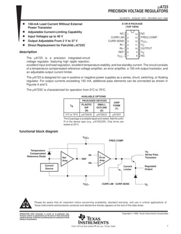
µA723PRECISION VOLTAGE REGULATORSSLVS057D – AUGUST 1972 – REVISED JULY 1999DDDDDD OR N PACKAGE(TOP VIEW)150-mA Load Current Without ExternalPower TransistorAdjustable Current-Limiting CapabilityInput Voltages up to 40 VOutput Adjustable From 2 V to 37 VDirect Replacement for Fairchild µA723CNCCURR LIMCURR SENSIN–IN REFVCC–description1142133124115106978NCFREQ COMPVCC VCOUTPUTVZNCThe µA723 is a precision integrated-circuitvoltage regulator, featuring high ripple rejection,excellent input and load regulation, excellent temperature stability, and low standby current. The circuit consistsof a temperature-compensated reference-voltage amplifier, an error amplifier, a 150-mA output transistor, andan adjustable-output current limiter.The µA723 is designed for use in positive or negative power supplies as a series, shunt, switching, or floatingregulator. For output currents exceeding 150 mA, additional pass elements can be connected as shown inFigures 4 and 5.The µA723C is characterized for operation from 0 C to 70 C.AVAILABLE OPTIONSPACKAGED DEVICESTAPLASTICDIP(N)SMALLOUTLINE(D)0 C to 70 CµA723CNµA723CDCHIPFORM(Y)µA723YThe D package is available taped and reeled. Add the suffixR to the device type (e.g., µA723CDR). Chip forms aretested at 25 C.functional block diagramVCC FREQ COMPIN–ErrorAmpREFIN RefAmpVCSeries PassTransistor–TemperatureCompensatedReference DiodeCurrentSourceCurrentLimiterVCC–CURR LIM CURR SENSRegulatedOutputVZPlease be aware that an important notice concerning availability, standard warranty, and use in critical applications ofTexas Instruments semiconductor products and disclaimers thereto appears at the end of this data sheet.Copyright 1999, Texas Instruments IncorporatedPRODUCTION DATA information is current as of publication date.Products conform to specifications per the terms of Texas Instrumentsstandard warranty. Production processing does not necessarily includetesting of all parameters.POST OFFICE BOX 655303 DALLAS, TEXAS 752651
µA723PRECISION VOLTAGE REGULATORSSLVS057D – AUGUST 1972 – REVISED JULY 1999schematicVCC 500 Ω1 kΩ25 kΩVC1 kΩ15 kΩ15 kΩOUTPUT6.2 V100 ΩVZ5 pF30 kΩFREQ COMP300 Ω5 kΩ150 Ω20 kΩCURR LIMCURR SENSREFIN VCC–IN–Resistor and capacitor values shown are nominal.absolute maximum ratings over operating free-air temperature range (unless otherwise noted)†Peak voltage from VCC to VCC– (tw 50 ms) . . . . . . . . . . . . . . . . . . . . . . . . . . . . . . . . . . . . . . . . . . . . . . . . . 50 VContinuous voltage from VCC to VCC– . . . . . . . . . . . . . . . . . . . . . . . . . . . . . . . . . . . . . . . . . . . . . . . . . . . . . . . 40 VInput-to-output voltage differential . . . . . . . . . . . . . . . . . . . . . . . . . . . . . . . . . . . . . . . . . . . . . . . . . . . . . . . . . . . . 40 VDifferential input voltage to error amplifier . . . . . . . . . . . . . . . . . . . . . . . . . . . . . . . . . . . . . . . . . . . . . . . . . . . . . 5 VVoltage between noninverting input and VCC– . . . . . . . . . . . . . . . . . . . . . . . . . . . . . . . . . . . . . . . . . . . . . . . . . . 8 VCurrent from VZ . . . . . . . . . . . . . . . . . . . . . . . . . . . . . . . . . . . . . . . . . . . . . . . . . . . . . . . . . . . . . . . . . . . . . . . . . 25 mACurrent from REF . . . . . . . . . . . . . . . . . . . . . . . . . . . . . . . . . . . . . . . . . . . . . . . . . . . . . . . . . . . . . . . . . . . . . . . . 15 mAPackage thermal impedance, θJA (see Notes 1 and 2): D package . . . . . . . . . . . . . . . . . . . . . . . . . . . . 86 C/WN package . . . . . . . . . . . . . . . . . . . . . . . . . . . 101 C/WLead temperature 1,6 mm (1/16 inch) from case for 10 seconds: D or N package . . . . . . . . . . . . . . . . 260 CStorage temperature range, Tstg . . . . . . . . . . . . . . . . . . . . . . . . . . . . . . . . . . . . . . . . . . . . . . . . . . . –65 C to 150 C† Stresses beyond those listed under “absolute maximum ratings” may cause permanent damage to the device. These are stress ratings only, andfunctional operation of the device at these or any other conditions beyond those indicated under “recommended operating conditions” is notimplied. Exposure to absolute-maximum-rated conditions for extended periods may affect device reliability.NOTES: 1. Maximum power dissipation is a function of TJ(max), θJA, and TA. The maximum allowable power dissipation at any allowableambient temperature is PD (TJ(max) – TA)/θJA. Operating at the absolute maximum TJ of 150 C can impact reliability.2. The package thermal impedance is calculated in accordance with JESD 51, except for through-hole packages, which use a tracelength of zero.2POST OFFICE BOX 655303 DALLAS, TEXAS 75265
µA723PRECISION VOLTAGE REGULATORSSLVS057D – AUGUST 1972 – REVISED JULY 1999recommended operating conditionsMINMAX9.540VOutput voltage, VO237VInput-to-output voltage differential, VC – VO338V150mA70 CInput voltage, VIOutput current, IOµA723COperating free-air temperature range, TA0UNITelectrical characteristics at specified free-air temperature (see Notes 3 and 4)PARAMETERTEST CONDITIONSTAVI 12 V to VI 15 VVI 12 V to VI 40 VInput regulationRipple rejectionµA723CMINTYPMAX25 C0.1125 C15VI 12 V to VI 15 Vf 50 Hz to 10 kHz,Cref 00 C to 70 C25 C74f 50 Hz to 10 kHz,Cref 5 µF25 C8625 C–0.3Output regulationStandby current25 CVI 30 V,IO 0Short-circuit output currentOutput noise voltage6.80 C to 70 CRSC 10 Ω,dB–2–625 CTemperature coefficient of output voltagemV/V30 C to 70 CReference voltage, VrefUNIT7.157.52.340.0030.015VO 0Cref 025 C65BW 100 Hz to 10 kHz,25 C20BW 100 Hz to 10 kHz,Cref 5 µF25 C2.5mV/VVmA%/ CmAµVNOTES: 3. For all values in this table, the device is connected as shown in Figure 1 with the divider resistance as seen by the error amplifier 10 kΩ. Unless otherwise specified, VI VCC VC 12 V, VCC– 0, VO 5 V, IO 1 mA, RSC 0, and Cref 0.4. Pulse-testing techniques must be used that will maintain the junction temperature as close to the ambient temperature as possible.electrical characteristics, TA 25 C (see Notes 3 and 4)PARAMETERInput regulationRipple rejectionTEST CONDITIONSVI 12 V to VI 15 VVI 12 V to VI 40 VµA723YMINTYP0.11f 50 Hz to 10 kHz,Cref 074f 50 Hz to 10 kHz,Cref 5 µF86MAXUNITmV/VdBOutput regulation–0.3mV/VReference voltage, Vref7.15V2.3mA65mAStandby currentShort-circuit output currentOutput noise voltageVI 30 V,RSC 10 Ω,IO 0VO 0BW 100 Hz to 10 kHz,Cref 020BW 100 Hz to 10 kHz,Cref 5 µF2.5µVNOTES: 3. For all values in this table, the device is connected as shown in Figure 1 with the divider resistance as seen by the error amplifier 10 kΩ. Unless otherwise specified, VI VCC VC 12 V, VCC– 0, VO 5 V, IO 1 mA, RSC 0, and Cref 0.4. Pulse-testing techniques must be used that will maintain the junction temperature as close to the ambient temperature as possible.POST OFFICE BOX 655303 DALLAS, TEXAS 752653
µA723PRECISION VOLTAGE REGULATORSSLVS057D – AUGUST 1972 – REVISED JULY 1999APPLICATION INFORMATIONTable 1. Resistor Values (kΩ) for Standard Output VoltagesOUTPUTVOLTAGE(V)APPLICABLEFIGURES(SEE NOTE 5)3.03.6FIXED OUTPUT 5%OUTPUT ADJUSTABLE 10%(SEE NOTE 6)R1(kΩ)R2(kΩ)R1(kΩ)P1(kΩ )P2(kΩ )1, 5, 6, 9, 11, 12 (4)4.123.011.80.51.21, 5, 6, 9, 11, 12 (4)3.573.651.50.51.55.01, 5, 6, 9, 11, 12 (4)2.154.990.750.52.26.01, 5, 6, 9, 11, 12 (4)1.156.040.50.52.79.02, 4, (5, 6, 9, 12)1.877.150.751.02.7122, 4, (5, 6, 9, 12)4.877.152.01.03.0152, 4, (5, 6, 9, 12)7.877.153.31.03.0282, 4, (5, 6, 9, e Note 7)3, 103.572.431.20.50.75–93, 103.485.361.20.52.0–123, 103.578.451.20.53.3–153, 103.5711.51.20.54.3–283, 95.32.21091–25083.572492.210240NOTES: 5. The R1/R2 divider can be across either VO or V(ref). If the divider is acrossV(ref), use the figure numbers without parentheses. If the divider is acrossVO, use the figure numbers in parentheses.6. To make the voltage adjustable, the R1/R2 divider shown in the figures mustbe replaced by the divider shown below.R1P1R2Adjustable Output Circuit7. For Figures 3, 8, and 10, the device requires a minimum of 9 V between VCC and VCC– when VO is equal to or more positive than –9 V.4POST OFFICE BOX 655303 DALLAS, TEXAS 75265
µA723PRECISION VOLTAGE REGULATORSSLVS057D – AUGUST 1972 – REVISED JULY 1999APPLICATION INFORMATIONTable 2. Formulas for Intermediate Output VoltagesOUTPUTS FROM 2 V TO 7 VSEE FIGURES 1, 5, 6, 9, 11, 12 (4)AND NOTE 5VO VOUTPUTS FROM 4 V TO 250 VSEE FIGURE 7 AND NOTE 5 V2R3 R4) R2R2(ref)R1OUTPUTS FROM 7 V TO 37 VSEE FIGURES 2, 4, (5, 6, 9, 11, 12)AND NOTE 5VO VR1(ref)(ref)VOR2 – R1R1I (limit)OUTPUTS FROM –6 V TO –250 VSEE FIGURES 3, 8, 10AND NOTES 5 AND 7 – V2R3 R4) R2(ref)VOR2CURRENT LIMITINGR1) R2V[ 0.65RSCFOLDBACK CURRENT LIMITINGSEE FIGURE 6I (knee)R1I OS[VOR3) (R3 ) R4) 0.65 VR SCR4V[ 0.65RSCR3) R4R4NOTES: 5. The R1/R2 divider can be across either VO or V(ref). If the divider is across V(ref), use figure numbers without parentheses. If thedivider is across VO, use the figure numbers in parentheses.7. For Figures 3, 8, and 10, the device requires a minimum of 9 V between VCC and VCC– when VO is equal to or more positive than–9 V.VIVCC REFR1VCOUTPUTµA723VZCURR LIMRSCRegulatedOutput, VOCURR SENSIN C(ref)VCC–IN–FREQ COMPR2NOTES: A. R3R2 R1R1 ) R2for a minimumaVR3 (see Notes A and B)100 pFOB. R3 can be eliminated for minimum component count. Use direct connection (i.e., R3 0).Figure 1. Basic Low-Voltage Regulator (VO 2 V to 7 V)POST OFFICE BOX 655303 DALLAS, TEXAS 752655
µA723PRECISION VOLTAGE REGULATORSSLVS057D – AUGUST 1972 – REVISED JULY 1999APPLICATION INFORMATIONVIVCC VCOUTPUTµA723REFVZCURR LIMR3(see Notes A and B)RSCRegulated Output,VOCURR SENSIN IN–FREQCOMPVCC–R1R2100 pFNOTES: A. R3R2 R1R1 ) R2for a minimumaVOB. R3 can be eliminated for minimum component count. Use direct connection (i.e., R3 0).Figure 2. Basic High-Voltage Regulator (VO 7 V to 37 V)VI2 kΩR2VCOUTPUTµA723VZREFCURR LIMVCC R4 3 kΩ2N5001CURR SENSIN–IN VCC– FREQ COMPR3 3 kΩR1100 pFFigure 3. Negative-Voltage Regulator6POST OFFICE BOX 655303 DALLAS, TEXAS 75265Regulated Output,VO
µA723PRECISION VOLTAGE REGULATORSSLVS057D – AUGUST 1972 – REVISED JULY 1999APPLICATION INFORMATIONVIVCVCC OUTPUTµA723VZCURR LIMREF2N3997CURR SENSRSCIN IN–VCC– FREQ COMPRegulated Output,VOR1500 pFR2Figure 4. Positive-Voltage Regulator (External npn Pass Transistor)VI60 Ω2N5001VCC OUTPUTµA723VZCURR LIMREFR1RSCCURR SENSIN VCC–R2VCRegulated Output,VOIN–FREQ COMP1000 pFFigure 5. Positive-Voltage Regulator (External pnp Pass Transistor)POST OFFICE BOX 655303 DALLAS, TEXAS 752657
µA723PRECISION VOLTAGE REGULATORSSLVS057D – AUGUST 1972 – REVISED JULY 1999APPLICATION INFORMATIONVIVCC R1VCRSCOUTPUTµA723REFVZCURR LIMR3CURR SENSR4IN IN–VCC– FREQ COMPRegulated Output,VOIOSVOlkneeIOR21000 pFFigure 6. Foldback Current LimitingVI2 kΩVCC 1N1826R4 3 kΩR3 3 kΩVC2N2580OUTPUTµA723REFVZCURR LIMR1CURR SENSIN IN–R2VCC– FREQ COMPRSC 1 Ω500 pFFigure 7. Positive Floating Regulator8POST OFFICE BOX 655303 DALLAS, TEXAS 75265Regulated Output,VO
µA723PRECISION VOLTAGE REGULATORSSLVS057D – AUGUST 1972 – REVISED JULY 1999APPLICATION INFORMATIONVI10 kΩVCC 1N759R2R3 3 kΩVC10 kΩOUTPUTµA723REFVZCURR LIM2N5287CURR SENSIN IN–VCC– FREQ COMPR1R4 3 kΩ500 pFRegulated Output,VOFigure 8. Negative Floating RegulatorVI3 kΩ2N51532N5005VCC REFR1IN R2OUTPUTµA723VZCURR LIML 1.2 mH(see Note A)51 ΩCURR SENS1 kΩ0.1 µFVC1 MΩRegulated Output,VOIN–VCC– FREQ COMP1N4005NOTE A: L is 40 turns of No. 20 enameled copper wire wound on Ferroxcube P36/22-3B7 potted core, or equivalent, with a 0.009-inch air gap.Figure 9. Positive Switching RegulatorPOST OFFICE BOX 655303 DALLAS, TEXAS 752659
µA723PRECISION VOLTAGE REGULATORSSLVS057D – AUGUST 1972 – REVISED JULY 1999APPLICATION INFORMATIONVI1 kΩ(see Note A)R3 3 kΩVCC R20.1 µFREF2N3997220 ΩVCOUTPUTµA723VZCURR LIM2N5004CURR SENS1 kΩIN R1IN–FREQCOMPVCC–1 MΩ15 pFR4 3 kΩL 1.2 mH(see Note B)1N4005100 µFRegulated Output,VONOTES: A. The device requires a minimum of 9 V between VCC and VCC– when VO is equal to or more positive than –9 V.B. L is 40 turns of No. 20 enameled copper wire wound on Ferroxcube P36/22-3B7 potted core, or equivalent, with a 0.009-inchair gap.Figure 10. Negative Switching RegulatorVIVCC R1VCRSCOUTPUTµA723REFVZCURR LIMRegulated Output,VOCURR SENSIN IN–VCC– FREQ COMPR22 kΩ2N44222 kΩ1000 pFInput FromSeries 54/74 LogicNOTE A: A current-limiting transistor can be used for shutdown if current limiting is not required.Figure 11. Remote Shutdown Regulator With Current Limiting10POST OFFICE BOX 655303 DALLAS, TEXAS 75265
µA723PRECISION VOLTAGE REGULATORSSLVS057D – AUGUST 1972 – REVISED JULY 1999APPLICATION INFORMATIONVIVCC REFR1IN 100 ΩVCOUTPUTµA723VZCURR LIM1 kΩ2N3997CURR SENSRegulated Output,VOIN–VCC– FREQ COMPR25000 pFFigure 12. Shunt RegulatorPOST OFFICE BOX 655303 DALLAS, TEXAS 7526511
PACKAGE OPTION ADDENDUMwww.ti.com14-Aug-2021PACKAGING INFORMATIONOrderable DeviceStatus(1)Package Type Package Pins PackageDrawingQtyEco Plan(2)Lead finish/Ball materialMSL Peak TempOp Temp ( C)Device Marking(3)(4/5)(6)UA723CDACTIVESOICD1450RoHS & GreenNIPDAULevel-1-260C-UNLIM0 to 70UA723CUA723CDE4ACTIVESOICD1450RoHS & GreenNIPDAULevel-1-260C-UNLIM0 to 70UA723CUA723CDRACTIVESOICD142500RoHS & GreenNIPDAULevel-1-260C-UNLIM0 to 70UA723CUA723CDRE4ACTIVESOICD142500RoHS & GreenNIPDAULevel-1-260C-UNLIM0 to 70UA723CUA723CDRG4ACTIVESOICD142500RoHS & GreenNIPDAULevel-1-260C-UNLIM0 to 70UA723CUA723CNACTIVEPDIPN1425RoHS & GreenNIPDAUN / A for Pkg Type0 to 70UA723CNUA723CNE4ACTIVEPDIPN1425RoHS & GreenNIPDAUN / A for Pkg Type0 to 70UA723CNUA723CNSRACTIVESONS142000RoHS & GreenNIPDAULevel-1-260C-UNLIM0 to 70UA723(1)The marketing status values are defined as follows:ACTIVE: Product device recommended for new designs.LIFEBUY: TI has announced that the device will be discontinued, and a lifetime-buy period is in effect.NRND: Not recommended for new designs. Device is in production to support existing customers, but TI does not recommend using this part in a new design.PREVIEW: Device has been announced but is not in production. Samples may or may not be available.OBSOLETE: TI has discontinued the production of the device.(2)RoHS: TI defines "RoHS" to mean semiconductor products that are compliant with the current EU RoHS requirements for all 10 RoHS substances, including the requirement that RoHS substancedo not exceed 0.1% by weight in homogeneous materials. Where designed to be soldered at high temperatures, "RoHS" products are suitable for use in specified lead-free processes. TI mayreference these types of products as "Pb-Free".RoHS Exempt: TI defines "RoHS Exempt" to mean products that contain lead but are compliant with EU RoHS pursuant to a specific EU RoHS exemption.Green: TI defines "Green" to mean the content of Chlorine (Cl) and Bromine (Br) based flame retardants meet JS709B low halogen requirements of 1000ppm threshold. Antimony trioxide basedflame retardants must also meet the 1000ppm threshold requirement.(3)MSL, Peak Temp. - The Moisture Sensitivity Level rating according to the JEDEC industry standard classifications, and peak solder temperature.(4)There may be additional marking, which relates to the logo, the lot trace code information, or the environmental category on the device.(5)Multiple Device Markings will be inside parentheses. Only one Device Marking contained in parentheses and separated by a " " will appear on a device. If a line is indented then it is a continuationof the previous line and the two combined represent the entire Device Marking for that device.Addendum-Page 1Samples
PACKAGE OPTION ADDENDUMwww.ti.com14-Aug-2021(6)Lead finish/Ball material - Orderable Devices may have multiple material finish options. Finish options are separated by a vertical ruled line. Lead finish/Ball material values may wrap to twolines if the finish value exceeds the maximum column width.Important Information and Disclaimer:The information provided on this page represents TI's knowledge and belief as of the date that it is provided. TI bases its knowledge and belief on informationprovided by third parties, and makes no representation or warranty as to the accuracy of such information. Efforts are underway to better integrate information from third parties. TI has taken andcontinues to take reasonable steps to provide representative and accurate information but may not have conducted destructive testing or chemical analysis on incoming materials and chemicals.TI and TI suppliers consider certain information to be proprietary, and thus CAS numbers and other limited information may not be available for release.In no event shall TI's liability arising out of such information exceed the total purchase price of the TI part(s) at issue in this document sold by TI to Customer on an annual basis.Addendum-Page 2
PACKAGE MATERIALS INFORMATIONwww.ti.com3-Jun-2022TAPE AND REEL INFORMATIONREEL DIMENSIONSTAPE DIMENSIONSK0P1B0 WReelDiameterCavityA0B0K0WP1A0Dimension designed to accommodate the component widthDimension designed to accommodate the component lengthDimension designed to accommodate the component thicknessOverall width of the carrier tapePitch between successive cavity centersReel Width (W1)QUADRANT ASSIGNMENTS FOR PIN 1 ORIENTATION IN TAPESprocket HolesQ1Q2Q1Q2Q3Q4Q3Q4User Direction of FeedPocket Quadrants*All dimensions are nominalDevicePackage Package PinsType DrawingSPQReelReelA0Diameter Width (mm)(mm) W1 (mm)B0(mm)K0(mm)P1(mm)WPin1(mm) Q1Pack Materials-Page 1
PACKAGE MATERIALS INFORMATIONwww.ti.com3-Jun-2022TAPE AND REEL BOX DIMENSIONSWidth (mm)WLH*All dimensions are nominalDevicePackage TypePackage DrawingPinsSPQLength (mm)Width (mm)Height 142000356.0356.035.0Pack Materials-Page 2
PACKAGE MATERIALS INFORMATIONwww.ti.com3-Jun-2022TUBET - TubeheightL - Tube lengthW - TubewidthB - Alignment groove width*All dimensions are nominalDevicePackage NamePackage TypePinsSPQL (mm)W (mm)T (µm)B A723CNE4NPDIP142550613.97112304.32Pack Materials-Page 3
IMPORTANT NOTICE AND DISCLAIMERTI PROVIDES TECHNICAL AND RELIABILITY DATA (INCLUDING DATA SHEETS), DESIGN RESOURCES (INCLUDING REFERENCEDESIGNS), APPLICATION OR OTHER DESIGN ADVICE, WEB TOOLS, SAFETY INFORMATION, AND OTHER RESOURCES “AS IS”AND WITH ALL FAULTS, AND DISCLAIMS ALL WARRANTIES, EXPRESS AND IMPLIED, INCLUDING WITHOUT LIMITATION ANYIMPLIED WARRANTIES OF MERCHANTABILITY, FITNESS FOR A PARTICULAR PURPOSE OR NON-INFRINGEMENT OF THIRDPARTY INTELLECTUAL PROPERTY RIGHTS.These resources are intended for skilled developers designing with TI products. You are solely responsible for (1) selecting the appropriateTI products for your application, (2) designing, validating and testing your application, and (3) ensuring your application meets applicablestandards, and any other safety, security, regulatory or other requirements.These resources are subject to change without notice. TI grants you permission to use these resources only for development of anapplication that uses the TI products described in the resource. Other reproduction and display of these resources is prohibited. No licenseis granted to any other TI intellectual property right or to any third party intellectual property right. TI disclaims responsibility for, and youwill fully indemnify TI and its representatives against, any claims, damages, costs, losses, and liabilities arising out of your use of theseresources.TI’s products are provided subject to TI’s Terms of Sale or other applicable terms available either on ti.com or provided in conjunction withsuch TI products. TI’s provision of these resources does not expand or otherwise alter TI’s applicable warranties or warranty disclaimers forTI products.TI objects to and rejects any additional or different terms you may have proposed. IMPORTANT NOTICEMailing Address: Texas Instruments, Post Office Box 655303, Dallas, Texas 75265Copyright 2022, Texas Instruments Incorporated
PRECISION VOLTAGE REGULATORS SLVS057D - AUGUST 1972 - REVISED JULY 1999 POST OFFICE BOX 655303 DALLAS, TEXAS 75265 3 recommended operating conditions MIN MAX UNIT Input voltage, VI 9.5 40 V Output voltage, V O 2 37 V Input-to-output voltage differential, V C - VO 3 38 V Output current, IO 150 mA