Transcription
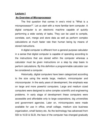
TI Designs: TIDA-015258-Channel, 16-Bit, 200-mA Current Output, Digital-toAnalog Converter Reference DesignDescriptionMany systems, such as optical laser drive applications,require flexible and precise current sources at a highchannel count. In addition, industry is moving tosmaller solutions as the number of required channelsincreases. This reference design combines the smallsize and high performance of the DAC80508 8channel, 16-bit DAC with precision op amps to createa high-density and accurate current source solution.The reference design has a maximum output currentof 200 mA, and allows for a minimal PVDD supplyvoltage in order to reduce power consumption for highefficiency. This reference design also features a lowcurrent-noise output because of the low referencevoltage noise of the DAC80508 and low voltage andcurrent noise of the OPA2376.Features Eight Channels of Programmable Current, 200-mARange 16-Bit Resolution High Channel-Density 120-µA Offset Error 1.5% Total Unadjusted Error 1.75-V Minimum PVDD Supply 3.4-µARMS Bandwidth-Limited Current Noise 10 nA/ Hz Current Noise at 10 kHzApplications Laser Drive in Optical Modules Tunable Laser Optical 4CSD23285F5Design FolderProduct FolderProduct FolderProduct FolderProduct FolderASK Our E2E ExpertsPVDDOPA376DAC80508ZIOUTOPA376LOADAn IMPORTANT NOTICE at the end of this TI reference design addresses authorized use, intellectual property matters and otherimportant disclaimers and information.TIDUDH4 – November 2018Submit Documentation Feedback8-Channel, 16-Bit, 200-mA Current Output, Digital-to-Analog ConverterReference DesignCopyright 2018, Texas Instruments Incorporated1
System Description1www.ti.comSystem DescriptionThe objective of this reference design is to demonstrate a compact high-side current-source design thatcan be implemented with a multichannel DAC, op amps, and discrete components. This design usescomponents that offer a high level of flexibility, and can be used in many different environments. The keycomponent of the design is the DAC80508 device. The device features eight DAC channels at 16-bitresolution that can be set to either a 1.25-V, 2.5-V, or 5-V range while using the internal reference. ThisDAC is a voltage-output device, so an external voltage-to-current (V/I) stage is added to the design. Toimplement the V/I stage, create an accurate reference current that is amplified using a current mirror.Laser-diode applications generally require a precisely controlled current to regulate the output power. Anadjustable current is advantageous because the laser output-power can shift over temperature. For thisreason, a DAC can be used to dynamically update the forward current. In addition, use a low-noise sourceto reduce the intensity noise (instability in the output power) of a laser output. The DAC 16-bit resolutionallows the power to be fine-tuned, but the same design could be used with the 14-bit DAC70508 and 12bit DAC60508 devices, which are pin-for-pin compatible with the DAC80508.1.1Key System SpecificationsTable 1. Key System nt-source supply voltage2 V, nominalSection 2.2.3DAC80508 and OPA2376 supply voltage5VSection 2.2.1DAC resolution and performance16-bit, 1 LSB INL/DNLSection 2.3.1Current-source full-scale output current200 mATotal unadjusted error 1.5% FSR at 25 CSection 3.2.2.1Current-noise density10 nA/ Hz at 10 kHz and full-scale outputSection 3.2.2.2Bandwidth limited RMS current noise3.4 µARMS at midscale outputSection 3.2.2.3Zero-scale error 120 µASection 3.2.2.4Minimum PVDD supply voltage1.75 V at full-scale outputSection 3.2.2.58-Channel, 16-Bit, 200-mA Current Output, Digital-to-Analog ConverterReference DesignCopyright 2018, Texas Instruments IncorporatedSection 2.2.3TIDUDH4 – November 2018Submit Documentation Feedback
System Overviewwww.ti.com2System Overview2.1Block DiagramFigure 1 shows a block diagram of the system.PVDDOPA376DAC80508ZIOUTOPA376LOADFigure 1. TIDA-01525 Block Diagram2.2Design ConsiderationsThis section describes the system, and the major subcircuits in the design. The system design can beconsidered to be made up of three main sections: the DAC stage, the V/I converter first stage, and the V/Iconverter second stage, as shown in Figure 2.PVDDISET2R22.0 kR3A4.99 kR3A4.99 kIMIRRFBAVDDCCMPAVDD0.1 F0.1 FRISOA20.1 FQ2 VIOOPA2376VIO VDD REFAVDD0.1 FVDACQ1 SECONDSTAGEA1SPIMASTEROPA2376RLOAD/DIODER14.99 kISET1DACSTAGEIOUTDAC80508ZFIRSTSTAGEFigure 2. TIDA-01525 Theory of OperationTIDUDH4 – November 2018Submit Documentation Feedback8-Channel, 16-Bit, 200-mA Current Output, Digital-to-Analog ConverterReference DesignCopyright 2018, Texas Instruments Incorporated3
System Overview2.2.1www.ti.comDAC Output StageFor this design, the DAC is configured externally with an SPI master. The voltage level of thecommunication is determined by VIO, which is supplied externally at 3.3 V. The analog portion of the DACis powered with AVDD, which is also shared with the op amps. For the purpose of the device testing, 5 Vis used for AVDD. The DAC80508 allows for 2.7 V minimum, whereas the OPA2376 can operate as lowas 2.2 V. Therefore, power consumption of AVDD can be reduced by operating at 2.7 V.The DAC80508 is configured to use the internal reference, which has an external 0.1-µF capacitor thathelps filter noise generated by the reference. The internal reference is the primary source of noise in thesystem, so an external, low-noise reference provides superior noise performance. However, an externallow-noise reference adds additional cost and board space to the system, so the external reference wasnot featured in this design.The DAC80508 features a reference attenuator that divides the reference by two. This setting is used bythe system to allow the maximum output range of the DAC to be 1.25 V. This lower voltage allows thePVDD supply to be minimized, and reduces the power dissipated by the output MOSFET, Q2.2.2.2First Op Amp StageThe first stage of the V/I circuit creates a reference current across sense resistor R1 in series with nchannel MOSFET Q1. By applying the DAC voltage output, VDAC, to the noninverting node of op amp A1.The device uses negative feedback to force the same voltage to the high-side of R1. The referencecurrent, ISET1, can be calculated with Equation 1.ISET1 VDAC R1NOTE:(1)The absolute value of the R1 influences the final output gain of the circuit, and anydifference between the real and ideal value appears as a gain error on the final outputcurrent. For this reason, make sure to select a precise resistor.The current generated by this stage does not contribute to the final output current; therefore, minimizingthis current is critical for optimizing the efficiency of the system. Power dissipated in the R1 can becalculated using Equation 2PR1 VDAC2 / R1(2)For this design, R1 is set to be 4.99 kΩ. When the DAC is at full-scale output voltage, ISET1 is calculated tobe approximately 250 µA, as shown in Equation 3:ISET1 FULL-SCALE 1.25 V 4.99 kΩ 250.5 µA2.2.3(3)Second Op Amp StageThe second stage of the system is a precision current-mirror with a gain set by R2 and R3. The voltageacross resistor R2 is determined by the reference current created by the first stage. Current ISET2 is ideallythe same as ISET1, and creates a voltage drop across R2. The voltage across R2 is the same voltageacross R3 because amplifier A2 uses p-channel MOSFET Q2 to draw the current from PVDD to makesure that the input nodes are the same potential. This relationship is shown in Equation 4:ISET1 R2 IMIR R3(4)The current gain of this system is then expressed by Equation 5:Current Gain IMIR ISET1 R2 R3(5)In this system, R2 is selected to be 2 kΩ and R3 is selected to be 2.495 Ω. This value is created in theapplication by using two resistors in parallel, which allows smaller resistors with lower power ratings to beused. Equation 6 shows the current gain given these resistor values.Current Gain 2 kΩ 2.495 Ω 801.6 A/A(6)The gain of the system can now be express using Equation 7:IOUT (VDAC R2) / (R1 R3)4(7)8-Channel, 16-Bit, 200-mA Current Output, Digital-to-Analog ConverterReference DesignCopyright 2018, Texas Instruments IncorporatedTIDUDH4 – November 2018Submit Documentation Feedback
System Overviewwww.ti.comUsing the values selected for the system, the full-scale output current can be calculated as shown inEquation 8:R1 4.99 kΩ, R2 2 kΩ, R3 2.495 ΩIOUT-MAX (1.25 V 2 kΩ) / (4.99 kΩ 2.495 Ω)IOUT-MAX 200.801 mA(8)(9)(10)There are a few sources of error in this stage. Firstly, the gain error of the stage is determined by how wellresistors R2 and R3 are proportionally matched; for this reason, use precision resistors. Secondly,amplifier A2 contributes to error with the voltage offset of the inputs. The offset results in a voltage acrossR2 that is not the same as the voltage across R3. This offset ultimately looks like an offset error on theoutput, and necessitates the selection of an amplifier that has low offset voltage. Finally, the bias currentof the amplifier causes the current flowing through R2, ISET2, to not exactly match the reference current,ISET1. This mismatch also results in an offset error on the output. Selecting an amplifier with a a biascurrent that is much lower than the reference current minimizes this error. The bias current also impactsthe IMIR current, but as that current is already very large, the impact is only a small offset error.For the reasons discussed, the OPA2376 is selected because this device has low bias current and offset,while still being a small package and capable of rail-to-rail operation.2.2.4PCB DesignWhite12.5 mmTOPLAYERFigure 3 shows the printed circuit board (PCB) layout of the TIDA-01525 design top and bottom layer. Thisboard has two internal layers: a ground layer and supply layer for PVDD. A majority of the PCB isdedicated to input and output headers that are necessary to improve the usability of the design duringtesting. The denoted box on the figure show the approximate area that was used on the top and bottomlayer to implement all eight channels of the design. The selection of small components and compactlayout result in a high-density design.BOTTOMLAYER20 mmInputHeaderOutputHeaderFigure 3. TIDA-01525 PCB DesignTIDUDH4 – November 2018Submit Documentation Feedback8-Channel, 16-Bit, 200-mA Current Output, Digital-to-Analog ConverterReference DesignCopyright 2018, Texas Instruments Incorporated5
System Overview2.2.5www.ti.comTINA-TI Simulation SoftwareThe output transfer function can be verified using the TINA-TI simulation software. Figure 4 shows thesimulation. The DAC80508 is simulated with an ideal voltage source for this experiment. Accurate modelsfor the OPA2376 and both MOSFETs are available at the product pages for those devices. Figure 5shows the simulated results, and verifies that the transfer function result is the expected full-scale outputcurrent.Figure 4. Simulation Using TINA-TI SoftwareFigure 5. IOUT Transfer Function TINA-TI Simulation Software Results68-Channel, 16-Bit, 200-mA Current Output, Digital-to-Analog ConverterReference DesignCopyright 2018, Texas Instruments IncorporatedTIDUDH4 – November 2018Submit Documentation Feedback
System Overviewwww.ti.com2.3Highlighted ProductsThe following highlighted products are used in this reference design. The key features for selecting thedevices for this reference design are outlined in the following subsections. For the complete details of thehighlighted devices, refer to the respective product data sheets. As many laser drive applications require ahigh channel density, a major factor in the component selection for this reference design is a smallpackage size. Figure 6 shows a relative comparison of the size of the major components of the system.0402 SMT PassiveComponent1.0 mm 0.5 mmCSD13381F4N-ChannelMOSFET1.0 mm 0.6 mmOPA2376AIYZDDual OPAMP2.3 mm 1.3 mmDAC80508ZYZF8-Channel DAC2.4 mm 2.4 mmCSD23285F5P-Channel MOSFET1.53 mm 0.77 mmFigure 6. Package Size Comparison2.3.1DAC80508The DAC80508 is a pin-compatible family of low-power, eight-channel, buffered voltage-output, digital-toanalog converters (DACs) with 16-bit resolution. The DAC80508 includes a 2.5-V, 5-ppm/ C internalreference that eliminates the need for an external precision reference in most applications. A userselectable gain configuration provides full-scale output voltages of 1.25 V (gain ½), 2.5 V (gain 1) or 5V (gain 2). The device operates from a single 2.7-V to 5.5-V supply, is specified monotonic, andprovides high linearity of 1 LSB INL.Communication to the DAC80508 is performed through a serial interface that operates at clock rates of upto 50 MHz. The VIO pin enables serial interface operation from 1.7 V to 5.5 V. The flexible interface of theDAC80508 enables operation with a wide range of industry-standard microprocessors andmicrocontrollers.The DAC80508 incorporates a power-on-reset circuit that powers up and maintains the DAC outputs ateither zero scale or midscale until a valid code is written to the device. The device consumes low currentof 0.6 mA/channel at 5.5 V, making the device suitable for battery-operated equipment. A per-channelpower-down feature reduces the device current consumption to 15 µA.The DAC80508 is characterized for operation over the temperature range of –40 C to 125 C, and isavailable in a 2.4-mm 2.4-mm WCSP package. This small package size makes this device an excellentchoice for high-density applications.TIDUDH4 – November 2018Submit Documentation Feedback8-Channel, 16-Bit, 200-mA Current Output, Digital-to-Analog ConverterReference DesignCopyright 2018, Texas Instruments Incorporated7
System Overview2.3.2www.ti.comOPA2376The OPA2376 is a dual, low-noise, e-trim operational amplifier that offers outstanding dc precision anddc performance. Rail-to-rail input and output, low offset (25 µV, maximum), low noise (7.5 nV/ Hz),quiescent current of 950 µA (maximum), and a 5.5-MHz bandwidth make this device very attractive for avariety of precision and portable applications. The PVDD supply used for the laser is often minimized toreduce power consumption of the MOSFET and resistor on the output stage of the design. Therefore, therail-to-rail output feature of the device makes it an excellent choice for the high-side current source forlaser-drive applications. This dual op amp is offered in a small, 2.3-mm 1.3-mm DSBGA package.2.3.3CSD13381F4 and CSD23285F5The FemtoFET MOSFETs in this design are selected because of their very small package size. TheCSD13381F4 is a 140-mΩ, 12-V N-channel MOSFET designed and optimized to minimize the footprint inmany handheld and mobile applications. The N-channel MOSFET is offered in a 1.0-mm 0.6-mmpackage. The CSD23285F5 is a 29-mΩ, –12-V, P-Channel MOSFET that features a 1.53-mm 0.77-mmpackage.88-Channel, 16-Bit, 200-mA Current Output, Digital-to-Analog ConverterReference DesignCopyright 2018, Texas Instruments IncorporatedTIDUDH4 – November 2018Submit Documentation Feedback
www.ti.comHardware, Software, Testing Requirements, and Test Results3Hardware, Software, Testing Requirements, and Test Results3.1Required Hardware3.1.1HardwareFigure 7 shows that the design hardware consists of the TIDA-01525 reference design PCB and a customtest bench PCB. The test bench allows for easier access to the supplies and current output connections.The test bench also enables the design PCB to remain very dense while still having the convenience ofconnectors for common lab equipment.Figure 7. Test BoardTIDUDH4 – November 2018Submit Documentation Feedback8-Channel, 16-Bit, 200-mA Current Output, Digital-to-Analog ConverterReference DesignCopyright 2018, Texas Instruments Incorporated9
Hardware, Software, Testing Requirements, and Test Results3.2www.ti.comTesting and Results3.2.1Test SetupThe test setup for this design features four pieces of external equipment.The National Instrument PXI-6289 features digital I/O used to generate the SPI data that control theDAC80508 device on the TIDA-01525 board. In addition, the digital I/O is used to control the MUXfeatured on the test board that connects the IOUT signals to external meters. Although not shown inFigure 8, the PXI-6289 18-bit ADC analog inputs are also connected to the IOUT signals. This connectionallows for fast parallel measurement of the IOUT signals, although higher levels of averaging must beimplemented to achieve very accurate measurements.The meter in this system is the Agilent 3458B, an 8.5-digit, digital multimeter (DMM). For the majority ofthe tests, the 3458B is configured to operate in a 1-V range, with two power-line cycles per acquisition.For some of the test, the DMM was removed from the system and replaced with an oscilloscope orspectrum analyzer.The system is powered by two supplies. The first supply, an Agilent E3631A triple-rail supply, is used topower the onboard MUX. To provide accurate measurements of the IOUT pins, the MUX needs additionalnegative headroom, so the negative supply input of the MUX is connected to a –5-V potential. The othersupply is a Keysight N6702A modular power supply mainframe. This supply sources the nominal 5-Vinput for the DAC80508 and OPA2376s featured in the design. The high-current PVDD supply was alsosourced from the N6702A. Take care to select a supply that can source the maximum expected current of1.6 A (8 channels 200 mA).Figure 8 shows that 4.7-Ω load resistors are used on the IOUT signals to convert the current output to avoltage for easy measurement with the 3458B. Given that our expected maximum current is approximately200 mA, a load of 4.7 Ω has a maximum voltage differential of 940 mV. This output range is optimized forthe DMM high-precision 1-V range.Keysight N6702APSUVDD 5 VAgilentE3631APSUPVDD 2 V8 5 Ví5 STLOADS4.7TEST BENCHBOARDFigure 8. Test Setup Block Diagram108-Channel, 16-Bit, 200-mA Current Output, Digital-to-Analog ConverterReference DesignCopyright 2018, Texas Instruments IncorporatedTIDUDH4 – November 2018Submit Documentation Feedback
Hardware, Software, Testing Requirements, and Test Resultswww.ti.com3.2.2Test ResultsThis section describes the test measurements accomplished on the system, and describes the setup andconfiguration used to realize them.3.2.2.13.2.2.1.1Total Unadjusted ErrorTotal Unadjusted Error Test ConfigurationTotal unadjusted error is measured on the system using the configuration shown in Figure 9. Totalunadjusted error, or TUE, is the difference between the actual measured transfer function of the systemand the ideal transfer function as calculated. This error is unadjusted; therefore, error from sources likeresistor mismatch, reference inaccuracy, and DAC nonlinearity are not removed from the calculation.The resistive values of the test loads must be accurately known, so that any error in those resistors is notrepresented in the measurement. To validate this condition, the individual resistance values were directlymeasured on the board and logged. The resistors must be directly measured so that the ON resistance ofthe MUX is not added to the resistor values. In addition, care must be taken to insulate these resistorsfrom temperature change during the test.The data for the measurement is collected by using the PXI-6289 to sweep the DAC80508 input code forall channels. After each code is sent to the DAC, the PXI-6289 sets the MUX to each channel, and the3458A measures the value. This value is then divided by the known resistor value of the test loads, andthe calculated current value is then logged. Make sure to allow a short time delay after changing the MUXinput to allow the output to settle.3.2.2.1.2Total Unadjusted Error Measurement ResultsTotal Unadjusted Error (%)Figure 9 shows the total unadjusted error for three systems, all channels. There are two main componentsto the error, offset error and gain error. The offset error is mostly the result of the DAC itself, with someadditional offset contributed by the VOS of the two amplifiers. The gain error can be attributed to the errorsin the resistor values, with the DAC reference also contributing a small portion. An external reference forthe DAC improves the accuracy, but at the expense of board space and additional -1.1-1.2-1.3-1.408192 16384 24576 32768 40960 49152 57344 65535DAC Code (LSB)D005Figure 9. Total Unadjusted ErrorTIDUDH4 – November 2018Submit Documentation Feedback8-Channel, 16-Bit, 200-mA Current Output, Digital-to-Analog ConverterReference DesignCopyright 2018, Texas Instruments Incorporated11
Hardware, Software, Testing Requirements, and Test Results3.2.2.23.2.2.2.1www.ti.comCurrent Noise DensityCurrent Noise Density Measurement SetupThe current noise density is measured with the National Instruments PXI-5922, a high-precisionoscilloscope. For this test configuration, the DAC80508 is programmed by the PXI-6289 to the full-scaleoutput current, 200 mA. The test board is configured to connect a channel through the MUX to the PXI5922, taking the place of the 3458B DMM. The PXI-5922 is then used to capture many thousands ofsamples for a few seconds, which are then processed by a program to generate a FFT of the data. Thisresult was also scaled back to a current value and converted to the power domain.3.2.2.2.2Current Noise Density ResultsThe current noise density is measured from 10 Hz to 100 kHz. The noise in the system is dominated bythe DAC80508 internal voltage reference. Using the internal reference results in the system being lesscomplex, and allows for cost savings; however, noise can be improved by using an external reference.10090Noise (nA/vHz)8070605040302010010 2030 50 100 200500 1000Frequency (Hz)10000100000D001tidaFigure 10. Current Noise Density3.2.2.33.2.2.3.1Bandwidth-Limited RMS Current NoiseBandwidth-Limited RMS Current Noise SetupThe bandwidth-limited RMS noise is measured in the same fashion as Figure 10, with additionalmeasurements at one-quarter scale and half scale. The RMS noise value is calculated from the noisespectral density. This calculation is achieved by integrating the square of the current noise spectral densityover the bandwidth of interest to calculate noise power. The RMS noise current is the square-root of thenoise power, which is the integral of the square of the noise density, as shown in Equation 11. In thiscase, the bandwidth of the measurement is limited from 10 Hz to 100 kHz.f2Noise CurrentNoise Power³ in2dff13.2.2.3.2(11)Bandwidth-Limited RMS Current Noise MeasurementTable 2 shows the calculated current noise based from the noise spectrum measurements at the differentDAC output values.Table 2. Bandwidth-Limited RMS Current Noise12DAC Output Code (LSB)Approximate Current Output (mA)Current Noise el, 16-Bit, 200-mA Current Output, Digital-to-Analog ConverterReference DesignCopyright 2018, Texas Instruments IncorporatedTIDUDH4 – November 2018Submit Documentation Feedback
Hardware, Software, Testing Requirements, and Test Resultswww.ti.com3.2.2.4Zero-Scale ErrorZero-scale error (ZSE) is the output current when the DAC is outputting the lowest possible value. TheDAC80508 features a unipolar supply input, meaning that the device does not have a negative supply. Asa result, the output at code zero is not 0 V, but rather the closest voltage the output buffer can supply withrespect to ground. ZSE can be critical in current-source applications, specifically laser-drive, because thezero-scale current can be considered wasted energy or even enable some low-power output state tooccur.3.2.2.4.1Zero-Scale Error SetupThe zero-scale error is measured by using the PXI-6289 to configure the DAC80508 device to the 1.25-Voutput range and configure the DAC values to code zero. The DMM is then used to measure the currenton the output of each channel. The ZSE is calculated as the difference between the real output currentand the ideal output current. The ZSE is easy to calculate because the ideal current at code zero is 0 A,so any current measured is entirely error.3.2.2.4.2Zero-Scale Error MeasurementCurrent Output (PA)The output behavior of the system is seen in Figure 11. As discussed previously, the DAC cannot output 0V, and requires a minimum headroom for the output buffer to accurately drive the output voltage.Figure 11 shows that the system requires approximately 64 LSB before the DAC can operate in the linearregion. Figure 12 shows the distribution of the zero-scale error for all eight channels of three systems. Themaximum voltage measured is below 120 µA of 2486480DAC Code (LSB)96112128D002Figure 11. IOUT Near Zero-Scale10987Count (Channels)76655433221100x000dx2020 d x4040 d x6060 d x8080 d x100100 d xZero-Scale Error (PA)120x t 120D006Figure 12. Zero-Scale Error MeasurementTIDUDH4 – November 2018Submit Documentation Feedback8-Channel, 16-Bit, 200-mA Current Output, Digital-to-Analog ConverterReference DesignCopyright 2018, Texas Instruments Incorporated13
Hardware, Software, Testing Requirements, and Test Results3.2.2.5www.ti.comMinimum PVDD Supply VoltageAny voltage headroom that is not necessary for the voltage drop across the load or diode and the voltageacross R3 results in extra power dissipation across the P-channel MOSFET. Therefore, a key design goalfor high-side current-sources in laser drive applications is to minimize the PVDD supply. However,minimizing PVDD can result in extra heat generation and general inefficiency. The minimum supplyvoltage is the lowest PVDD voltage the system can use while still being able to source the desired fullscale current.3.2.2.5.1Minimum PVDD Supply Voltage SetupThe minimum supply voltage was measured by using the PXI-6289 to set the DAC output to the full-scalevalue, 0xFFFF, or approximately 200 mA on the current output. While in this state, the DMM is used tomeasure the current output, while the N6702A is used to incrementally lower the PVDD supply. The fullscale current error is calculated at each point. At some point, the system cannot source the correct currentand the FSE rapidly changes.3.2.2.5.2Minimum PVDD Supply Voltage MeasurementFigure 13 shows the FSE as the PVDD is varied from 1.5 V to 4 V. Figure 13 shows that the FSE isrelatively constant until the PVDD supply becomes less than 1.75 V. This This supply voltage is theminimum required headroom voltage for the system. The voltage across R1 will be 1.25 V unless the DACrange is modified, and the reference current created induces a voltage of approximately 500 mV acrossR2. These two voltages make the required 1.75 V, as shown in Figure 13. If lower voltage (and powerdissipation) is desired, scale back the resistor values of R2 and R3 to a lower value, while still maintainingthe same ratio.2Full-Scale Error (%FSR)10-1-2-3-41.51.7522.252.5 2.75 3PVDD (V)3.253.53.754D004Figure 13. Minimum PVDD Voltage148-Channel, 16-Bit, 200-mA Current Output, Digital-to-Analog ConverterReference DesignCopyright 2018, Texas Instruments IncorporatedTIDUDH4 – November 2018Submit Documentation Feedback
Design Fileswww.ti.com4Design Files4.1Altium Files4.1.1SchematicsTo download the schematics, see the design files at TIDA-01525.4.1.2Bill of MaterialsTo download the bill of materials (BOM), see the design files at TIDA-01525.4.1.3PCB Layout RecommendationsWhen designing the PCB for the reference circuit, consider the following layout recommendations: Place the capacitor for the DAC80508 reference output close to the pin in order to minimize externalnoise from being coupled into the reference voltage. Bypass all power supply pins to ground with a low ESR ceramic bypass capacitor. The typicalrecommended bypass capacitance is 0.1-µF to 0.22-µF ceramic with a X7R or NP0 dielectric. Use wider trace widths for the current output path that can accommodate the full-scale current. Connect R3 to a large copper area to assist in heat dissipation.4.1.3.1Layout PrintsTo download the layer plots, see the design files at TIDA-01525.4.2Gerber FilesTo download the Gerber files, see the design files at TIDA-01525.4.3Assembly DrawingsTo download the assembly drawings, see the design files at TIDA-01525.5Related Documentation1. High-Side Voltage-to-Current (V-I) Converter Design Guide2. High-Density DACs Offer Superior Noise And Accuracy Performance in Laser-Drive ApplicationsApplication Brief5.1TrademarksTINA-TI, e-trim, FemtoFET are trademarks of Texas Instruments.All other trademarks are the property of their respective owners.6About the AuthorPaul Frost is an Applications Engineer with the Digital to Analog Converters team supporting catalog,industrial, and audio DACs. He earned his BSCE from University of Arizona.TIDUDH4 – November 2018Submit Documentation Feedback8-Channel, 16-Bit, 200-mA Current Output, Digital-to-Analog ConverterReference DesignCopyright 2018, Texas Instruments Incorporated15
IMPORTANT NOTICE AND DISCLAIMERTI PROVIDES TECHNICAL AND RELIABILITY DATA (INCLUDING DATASHEETS), DESIGN RESOURCES (INCLUDING REFERENCEDESIGNS), APPLICATION OR OTHER DESIGN ADVICE, WEB TOOLS, SAFETY INFORMATION, AND OTHER RESOURCES “AS IS”AND WITH ALL FAULTS, AND DISCLAIMS ALL WARRANTIES, EXPRESS AND IMPLIED, INCLUDING WITHOUT LIMITATION ANYIMPLIED WARRANTIES OF MERCHANTABILITY, FITNESS FOR A PARTICULAR PURPOSE OR NON-INFRINGEMENT OF THIRDPARTY INTELLECTUAL PROPERTY RIGHTS.These resources are intended for skilled developers designing with TI products. You are solely responsible for (1) selecting the appropriateTI products for your application, (2) designing, validating and testing your application, and (3)
This DAC is a voltage-output device, so an external voltage-to-current (V/I) stage is added to the design. To implement the V/I stage, create an accurate reference current that is amplified using a current mirror. Laser-diode applications generally require a precisely controlled current to regulate the output power.