Transcription
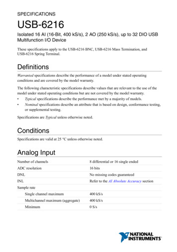
SPECIFICATIONSUSB-6216Isolated 16 AI (16-Bit, 400 kS/s), 2 AO (250 kS/s), up to 32 DIO USBMultifunction I/O DeviceThese specifications apply to the USB-6216 BNC, USB-6216 Mass Termination, andUSB-6216 Spring Terminal.DefinitionsWarranted specifications describe the performance of a model under stated operatingconditions and are covered by the model warranty.The following characteristic specifications describe values that are relevant to the use of themodel under stated operating conditions but are not covered by the model warranty. Typical specifications describe the performance met by a majority of models. Nominal specifications describe an attribute that is based on design, conformance testing,or supplemental testing.Specifications are Typical unless otherwise noted.ConditionsSpecifications are valid at 25 C unless otherwise noted.Analog InputNumber of channels8 differential or 16 single endedADC resolution16 bitsDNLNo missing codes guaranteedINLRefer to the AI Absolute Accuracy sectionSample rateSingle channel maximum400 kS/sMultichannel maximum (aggregate)400 kS/sMinimum0 S/s
Timing resolution50 nsTiming accuracy50 ppm of sample rateInput couplingDCInput range 0.2 V, 1 V, 5 V, 10 VMaximum working voltage for analoginputs (signal common mode) 10.4 V of AI GNDCMRR (DC to 60 Hz)100 dBInput impedanceDevice onAI to AI GND 10 GΩ in parallel with 100 pFAI- to AI GND 10 GΩ in parallel with 100 pFDevice offAI to AI GND1,200 ΩAI- to AI GND1,200 ΩInput bias current 100 pACrosstalk (at 100 kHz)Adjacent channels-75 dBNon-adjacent channels-90 dBSmall signal bandwidth (-3 dB)1.5 MHzInput FIFO size4,095 samplesScan list memory4,095 entriesData transfersUSB Signal Stream, programmed I/OOvervoltage protection for all analog input and sense channelsDevice on 30 V for up to two AI pinsDevice off 20 V for up to two AI pinsInput current during overvoltage condition 20 mA maximum/AI pinSettling Time for Multichannel MeasurementsAccuracy, full-scale step, all ranges2 90 ppm of step ( 6 LSB)2.5 μs convert interval 30 ppm of step ( 2 LSB)3.5 μs convert interval 15 ppm of step ( 1 LSB)5.5 μs convert intervalni.com USB-6216 Specifications
Typical Performance GraphsFigure 1. Settling Error versus Time for Different Source ImpedancesError (ppm of Step Size)10 k1k100 1 kΩ2 kΩ5 kΩ10 kΩ101110100Time (µs)Figure 2. AI CMRR140CMRR (dB)12010080604060 1001k10 k100 kFrequency (Hz)AI Absolute Accuracy (Warranted)Note Accuracies listed are valid for up to one year from the device externalcalibration.Note The input/output channels of this device are not protected for electromagneticinterference due to functional reasons. As a result, this device may experienceUSB-6216 Specifications National Instruments 3
reduced measurement accuracy or other temporary performance degradation whenconnected cables are routed in an environment with radiated or conducted radiofrequency electromagnetic interference. To ensure that this device functions withinspecifications in its operational electromagnetic environment and to limit radiatedemissions, care should be taken in the selection, design, and installation ofmeasurement probes and cables.Table 1. AI Absolute AccuracyNominal Nominal Residual Positive NegativeErrorErrorTempco Randomat FullFullFull(ppm of (ppm of(ppm ofNoise, σScaleSensitivityScaleScaleReading) Range) Range/ C) 5.2Note Sensitivity is the smallest voltage change that can be detected. It is a functionof noise.Gain tempco7.3 ppm/ CReference tempco5 ppm/ CINL error76 ppm of rangeAI Absolute Accuracy EquationAbsoluteAccuracy Reading · (GainError) Range · (OffsetError) NoiseUncertaintyGainError ResidualAIGainError GainTempco · (TempChangeFromLastInternalCal) ReferenceTempco · (TempChangeFromLastExternalCal)OffsetError ResidualAIOffsetError OffsetTempco ·(TempChangeFromLastInternalCal) INLErrorNoiseUncertainty 100 points.Random Noise 3for a coverage factor of 3 σ and averaging100AI Absolute Accuracy ExampleAbsolute accuracy at full scale on the analog input channels is determined using the followingassumptions: TempChangeFromLastExternalCal 10 C TempChangeFromLastInternalCal 1 C4 ni.com USB-6216 Specifications
number of readings 100CoverageFactor 3 σFor example, on the 10 V range, the absolute accuracy at full scale is as follows:GainError 75 ppm 7.3 ppm · 1 5 ppm · 10 132 ppmOffsetError 20 ppm 34 ppm · 1 76 ppm 130 ppmNoiseUncertainty 295 µ 3 88.5 µV100AbsoluteAccuracy 10 V · (GainError) 10 V · (OffsetError) NoiseUncertainty 2,710 µVAnalog OutputNumber of channels2DAC resolution16 bitsDNL 1 LSBMonotonicity16 bit guaranteedMaximum update rate1 channel250 kS/s2 channels250 kS/s per channelTiming accuracy50 ppm of sample rateTiming resolution50 nsOutput range 10 VOutput couplingDCOutput impedance0.2 ΩOutput current drive 2 mAOverdrive protection 30 VOverdrive current2.4 mAPower-on state 20 mVPower-on glitch 1 V for 200 msOutput FIFO size8,191 samples shared among channels usedData transfersUSB Signal Stream, programmed I/OAO waveform modesNon-periodic waveform, periodic waveformregeneration mode from onboard FIFO,periodic waveform regeneration from hostbuffer including dynamic updateUSB-6216 Specifications National Instruments 5
Settling time, full-scale step,15 ppm (1 LSB)32 µsSlew rate5 V/µsGlitch energyMagnitude100 mVDuration2.6 µsAO Absolute Accuracy (Warranted)Absolute accuracy at full-scale numbers is valid immediately following internal calibrationand assumes the device is operating within 10 C of the last external calibration.Note Accuracies listed are valid for up to one year from the device externalcalibration.Note The input/output channels of this device are not protected for electromagneticinterference due to functional reasons. As a result, this device may experiencereduced measurement accuracy or other temporary performance degradation whenconnected cables are routed in an environment with radiated or conducted radiofrequency electromagnetic interference. To ensure that this device functions withinspecifications in its operational electromagnetic environment and to limit radiatedemissions, care should be taken in the selection, design, and installation ofmeasurement probes and cables.Table 2. AO Absolute AccuracyNominalRangePositiveFull Scale(V)NominalRangeNegativeFull Scale(V)ResidualGain Error(ppm ofReading)GainTempco(ppm/ C)ResidualOffsetError (ppmof Range)OffsetTempco(ppm ofRange/ C)AbsoluteAccuracyat FullScale (μV)10-10901160123,512Reference tempco5 ppm/ CINL error128 ppm of rangeAO Absolute Accuracy EquationAbsoluteAccuracy OutputValue · (GainError) Range · (OffsetError)GainError ResidualGainError GainTempco · (TempChangeFromLastInternalCal) ReferenceTempco · (TempChangeFromLastExternalCal)OffsetError ResidualOffsetError AOOffsetTempco ·(TempChangeFromLastInternalCal) INLError6 ni.com USB-6216 Specifications
Digital I/O and PFIStatic Digital I/O CharacteristicsDigital input or outputBNC/Mass Termination24 total, 8 (P0. 0.7 ),16 (PFI 0.7 /P1. 0.7 ,PFI 8.15 /P2. 0.7 )Screw Terminal32 total, 16 (P0. 0.15 ),16 (PFI 0.7 /P1. 0.7 ,PFI 8.15 /P2. 0.7 )Ground referenceD GNDPull-down resistor50 kΩ typical, 20 kΩ minimumInput voltage protection 20 V on up to 8 pins1PFI FunctionalityFunctionalityStatic digital input, static digital output, timinginput, timing outputTiming output sourcesMany AI, AO, counter timing signalsDebounce filter settings125 ns, 6.425 µs, 2.56 ms, disable; high andlow transitions; selectable per inputMaximum Operating ConditionsIOL output low current16 mA maximumIOH output high current-16 mA maximumDigital Input CharacteristicsLevelMinimumMaximumVIL input low voltage0V0.8 VVIH input high voltage2.2 V5.25 VIIL input low current (Vin 0 V)--10 μAIIH input high current (Vin 5 V)-250 μA1Stresses beyond those listed under Input voltage protection may cause permanent damage to thedevice.USB-6216 Specifications National Instruments 7
LevelMinimumMaximumPositive-going threshold (VT )-2.2 VNegative-going threshold (VT-)0.8 V-Delta VT hysteresis (VT - VT-)0.2 V-Digital Output CharacteristicsFigure 3. PFI 0.15 /P0. 0.15 : Ioh versus Voh055 C; Vdd 4.5 V25 C; Vdd 5.0 V0 C; Vdd 5.5 V–5–10IOH (mA)–15–20–25–30–35–40–45–50234VOH (V)8 ni.com USB-6216 Specifications56
Figure 4. PFI 0.15 /P0. 0.15 : Iol versus Vol4055 C; Vdd 4.5 V25 C; Vdd 5.0 V0 C; Vdd 5.5 V3530Iol (mA)252015105000.20.40.60.811.2Vol (V)General-Purpose Counters/TimersNumber of counter/timers2Resolution32 bitsCounter measurementsEdge counting, pulse, semi-period, period,two-edge separationPosition measurementsX1, X2, X4 quadrature encoding withChannel Z reloading; two-pulse encodingOutput applicationsPulse, pulse train with dynamic updates,frequency division, equivalent time samplingInternal base clocks80 MHz, 20 MHz, 0.1 MHzExternal base clock frequency0 MHz to 20 MHzBase clock accuracy50 ppmInputsGate, Source, HW Arm, Aux, A, B, Z,Up DownRouting options for inputsPFI 0.15 , many internal signalsFIFO1,023 samplesData transfersUSB Signal Stream, programmed I/OUSB-6216 Specifications National Instruments 9
Frequency GeneratorNumber of channels1Base clocks10 MHz, 100 kHzDivisors1 to 16Base clock accuracy50 ppmOutput can be available on any output PFI terminal.External Digital TriggersSourcePFI 0.15 PolaritySoftware-selectable for most signalsAnalog input functionStart Trigger, Reference Trigger,Pause Trigger, Sample Clock, Convert Clock,Sample Clock TimebaseAnalog output functionStart Trigger, Pause Trigger, Sample Clock,Sample Clock TimebaseCounter/timer functionGate, Source, HW Arm, Aux, A, B, Z,Up DownBus InterfaceUSBUSB 2.0 Hi-Speed or full-speed2USB Signal Stream4, can be used for analog input, analog output,counter/timer 0, counter/timer 1Current Limits 5 V terminal as output32310 Voltage4.6 V to 5.2 VCurrent (internally limited)50 mA maximum, shared with digital outputsIf you are using an USB M Series device in full-speed mode, device performance will be lower andyou will not be able to achieve maximum sample/update rates.USB Screw Terminal/BNC devices have a self-resetting fuse that opens when current exceeds thisspecification. USB Mass Termination devices have a user-replaceable socketed fuse that openswhen current exceeds this specification. Refer to the NI USB-621x User Manual for informationabout fuse replacement.ni.com USB-6216 Specifications
5 V terminal as input3Voltage4.75 V to 5.35 VCurrent350 mA maximum, self-resetting fuseCaution Do not exceed 16 mA per DIO pin.Protection 10 VPower RequirementsInput voltage on USB port4.5 V to 5.25 V in configured stateMaximum inrush current500 mANo load typical current320 mA at 4.5 VMaximum loadTypical current400 mA at 4.5 VSuspend current260 μA typicalPhysical CharacteristicsDimensions (includes connectors)BNC23.5 cm 11.2 cm 6.4 cm(9.25 in. 4.40 in. 2.50 in.)Mass Termination19.3 cm 9.4 cm 3.1 cm(7.61 in. 3.68 in. 1.20 in.)Screw Terminal16.9 cm 9.4 cm 3.1 cm(6.65 in. 3.70 in. 1.20 in.)WeightBNC950 g (33.5 oz)Mass Termination231 g (8.1 oz)Screw Terminal206 g (7.2 oz)I/O connectorsBNC19 BNCs and 26 screw terminalsMass Termination1 68-pin SCSIScrew Terminal4 16-position combiconUSB-6216 Specifications National Instruments 11
Screw terminal wiring16 AWG to 28 AWGTorque for screw terminals0.22 N · m to 0.25 N · m(2.0 lb · in. to 2.2 lb · in.)USB connectorSeries B receptacleTo clean the device, wipe with a dry towel.CalibrationRecommended warm-up time15 minutesCalibration interval1 yearEnvironmentalOperating temperature0 ºC to 45 ºCStorage temperature-20 ºC to 70 ºCHumidity10% RH to 90% RH, noncondensingMaximum altitude2,000 mPollution Degree2Indoor use only.Safety VoltagesConnect only voltages that are below these limits.Channel-to-earth ground4Continuous 60 VDC Measurement Category IWithstand 1,000 Vrms, verified by a 5 s dielectricwithstand testAnalog channel-to-AI GND or AO GND(in the following figure, Va - Vc ) 11 V, Measurement Category IDigital channel-to-D GND (in thefollowing figure, Vb - Vc ) 5.25 V, Measurement Category IMeasurement Category I is for measurements performed on circuits not directly connected tothe electrical distribution system referred to as MAINS voltage. MAINS is a hazardous liveelectrical supply system that powers equipment. This category is for measurements of voltages412 In the figure, Va – Vd , Vb – Vd , and Vc – Vd .ni.com USB-6216 Specifications
from specially protected secondary circuits. Such voltage measurements include signal levels,special equipment, limited-energy parts of equipment, circuits powered by regulated lowvoltage sources, and electronics.Caution This device is rated for Measurement Category I and the voltage acrossthe isolation barrier is limited to no greater than 30 Vrms/60 VDC/42.4 Vpkcontinuous. Do not use for measurements within Measurement Categories CAT II,CAT III, or CAT IV.Note Measurement Categories CAT I and CAT O (Other) are equivalent. These testand measurement circuits are not intended for direct connection to the MAINSbuilding installations of Measurement Categories CAT II, CAT III, or CAT IV.The following figure illustrates the safety voltages specifications.Figure 5. USB-6216 Safety VoltagesIsolated Front EndVaAI x/AO xVbPFI xVcAI GND/AO GND/D GNDUSB ConnectorBusIsolation BarrierVeBusVdSafetyThis product is designed to meet the requirements of the following electrical equipment safetystandards for measurement, control, and laboratory use: IEC 61010-1, EN 61010-1 UL 61010-1, CSA C22.2 No. 61010-1Note For UL and other safety certifications, refer to the product label or the OnlineProduct Certification section.USB-6216 Specifications National Instruments 13
Electromagnetic CompatibilityThis product meets th
USB-6216 Isolated 16 AI (16-Bit, 400 kS/s), 2 AO (250 kS/s), up to 32 DIO USB Multifunction I/O Device These specifications apply to the USB-6216 BNC, USB-6216 Mass Termination, and USB-6216 Spring Terminal. Definitions Warranted specifications describe the performance of a model under stated operating conditions and are covered by the model warranty.
