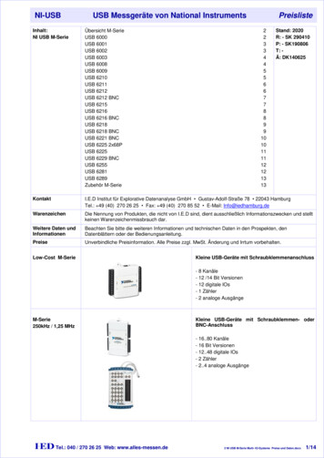
Transcription
High Speed USB Design Guidelines1. IntroductionThis document provides guidelines for integrating a AT85C51SND3Bx high speedUSB device controller onto a 4-layer PCB. The material covered can be broken intotwo main categories: board design guidelines and layout examples.High speed USB operation is described in the USB 2.0 tml).AT85C51SND3BxMicrocontrollersApplication Note7633A–MP3–06/06
2. Layout Guidelines2.1General Routing and PlacementUse the following general routing and placement guidelines when laying out a new design.These guidelines will help to minimize signal quality problems.1. Place the high-speed USB host controller and major components on the unrouted board.2. With minimum trace lengths, route high-speed clock and high-speed USB differential pairs.Maintain maximum possible distance between high-speed clocks/periodic signals to highspeed USB differential pairs and any connector leaving the PCB (such as, I/O connectors,control and signal headers, or power connectors).3. Route high-speed USB signals using a minimum of vias and corners. This reduces signalreflections and impedance changes.4. When it becomes necessary to turn 90 , use two 45 turns or an arc instead of making asingle 90 turn. This reduces reflections on the signal by minimizing impedancediscontinuities.5. Do not route USB traces under crystals, oscillators, clock synthesizers, magnetic devicesor ICs that use and/or duplicate clocks.6. Stubs on high speed USB signals should be avoided, as stubs will cause signal reflectionsand affect signal quality.7. Route all traces over continuous GND plane with no interruptions.2.2High Speed USB Trace SpacingFigure 2-1 provides an illustration of the recommended trace spacing while Table 2-1 givessome trace calculation examples. Use the following guidelines.1. Use an impedance calculator to determine the trace width (W) and spacing (S) required forthe specific board stack-up being used. W is calculated to achieve a trace impedance (Z0)of 50W and S is calculated to achieve a differential trace impedance of 90W. Theseimpedances depend in first approximation on the following PCB parameters delivered bythe PCB manufacturer:–er: dielectric relative permittivity– H: dielectric height– T: trace thickness2. Maintain parallelism between USB differential signals with the trace spacing calculated toachieve 90W differential impedance. Deviations will normally occur due to package breakout and routing to connector pins. Ensure the amount and length of the deviations are keptto the minimum.3. Minimize the length of high-speed clock and periodic signal traces that run parallel to highspeed USB signal lines to minimize crosstalk. Based on EMI testing experience, the minimum suggested spacing to clock signals is 50 mils.4. Based on simulation data, use 20-mil minimum spacing between high-speed USB signalpairs and other signal traces for optimal signal quality. This helps to prevent crosstalk.27633A–MP3–06/06
Figure 2-1.Recommended Trace SpacingLow speed/non periodicsignal20 milsWDMH50 milsWSDPHHigh speed/clock periodicsignalTεHDielectric ( r)USB Analog Ground PlaneTable 2-1.Trace Characteristics ExamplesPCB Characteristics2.3Trace 51.47.57.53.95.51.71010High Speed USB TerminationAT85C51SND3Bx high-speed USB design requires 39 W termination resistor at both DPH andDMH pins. Place the termination resistors as close as possible to the AT85C51SND3Bx signalpins.2.4High Speed USB Trace Length MatchingHigh-speed USB signal pair traces should be trace-length matched. Max trace-length mismatchbetween high-speed USB signal pairs should be no greater than 150 mils.2.5High Speed USB Bias FilterAT85C51SND3Bx high-speed USB design requires a 6.81KW 1% resistor in parallel to a 10pFcapacitor connected from UBIAS pin to USB ground. The resistor defines the master biasing ofthe AT85C51SND3Bx high-speed pad and should be placed as close as possible to the UBIASpin by taking care to minimize noise injection at this point.2.6High Speed USB ESD ProtectionFull-speed USB provide ESD suppression using in-line ferrites and capacitors that form a lowpass filter. This technique doesn’t work for high-speed USB due to the much higher signal rate ofhigh-speed data. A recommended device that has been tested successfully is a LittelFuse component, PulseGuard PGB0010603MR (0603 package size). Proper placement of thedevices is on the data lines as close as possible to the USB connector. Other low-capacitanceESD protection devices may work as well. We recommend including the footprints for thisdevice, or some other proven solution, as a stuffing option in case it is needed to pass ESD testing and in the event that a problem occurs (general routing and placement guidelines should befollowed).37633A–MP3–06/06
2.7High Speed USB ConnectorsIn order to provide direct connection of high-speed USB signals, we recommend to use throughh o l e m i n i - A B o r s u r f a c e m ou n t r ev e r s e d m in i - A B r ec e p t a c l e c o n n e c t o r. I n c a s eAT85C51SND3Bx OTG capability is not requested, we recommend to use through hole mini-Bor surface mount reversed mini-B receptacle connector or surface mount std-A plug.3. Layout ExamplesFigure 3-1 to Figure 3-3 show some examples of AT85C51SND3Bx high-speed USB routing. Inorder to allow direct connection to AT89C51SND3 controller, a reversed mini-AB connector isbetter used to avoid via and signal ed Mini AB Receptacle - USB Routing ExampleDMFDPFUVSSFigure 3-1.Bias FilterUSB AnalogGround PlaneESDProtectionsVBUSconnectionVias to USBground plane5 4 3 2 1Reversed Mini AB47633A–MP3–06/06
TerminationResistorsDPHDMHUVSSUBIASReversed Mini AB Receptacle - USB Routing ExampleDMFDPFUVSSFigure 3-2.Bias FilterUSB AnalogGround PlaneESDProtectionsVBUSconnectionVias to USBground plane5 4 3 2 1Reversed Mini AB57633A–MP3–06/06
Figure 3-3.Standard Mini AB Receptacle - USB Routing ASBias FilterUSB AnalogGround PlaneESDProtectionsVBUSconnectionVias to USBground plane1 2 3 4 5Standard Mini ABTop67633A–MP3–06/06
DPHDMHUVSSUBIASStandard Mini AB Receptacle - USB Routing ExampleDMFDPFUVSSFigure 3-4.TerminationResistorsVias to bottomBias FilterUSB AnalogGround PlaneVBUSconnectionVias to USBground plane5 4 3 2 1Standard Mini ABBottom77633A–MP3–06/06
Atmel Corporation2325 Orchard ParkwaySan Jose, CA 95131, USATel: 1(408) 441-0311Fax: 1(408) 487-2600Regional HeadquartersEuropeAtmel SarlRoute des Arsenaux 41Case Postale 80CH-1705 FribourgSwitzerlandTel: (41) 26-426-5555Fax: (41) 26-426-5500AsiaRoom 1219Chinachem Golden Plaza77 Mody Road TsimshatsuiEast KowloonHong KongTel: (852) 2721-9778Fax: (852) 2722-1369Japan9F, Tonetsu Shinkawa Bldg.1-24-8 ShinkawaChuo-ku, Tokyo 104-0033JapanTel: (81) 3-3523-3551Fax: (81) 3-3523-7581Atmel OperationsMemory2325 Orchard ParkwaySan Jose, CA 95131, USATel: 1(408) 441-0311Fax: 1(408) 436-4314RF/AutomotiveTheresienstrasse 2Postfach 353574025 Heilbronn, GermanyTel: (49) 71-31-67-0Fax: (49) 71-31-67-2340Microcontrollers2325 Orchard ParkwaySan Jose, CA 95131, USATel: 1(408) 441-0311Fax: 1(408) 436-4314La ChantrerieBP 7060244306 Nantes Cedex 3, FranceTel: (33) 2-40-18-18-18Fax: (33) 2-40-18-19-60ASIC/ASSP/Smart CardsZone Industrielle13106 Rousset Cedex, FranceTel: (33) 4-42-53-60-00Fax: (33) 4-42-53-60-011150 East Cheyenne Mtn. Blvd.Colorado Springs, CO 80906, USATel: 1(719) 576-3300Fax: 1(719) 540-1759Biometrics/Imaging/Hi-Rel MPU/High Speed Converters/RF DatacomAvenue de RochepleineBP 12338521 Saint-Egreve Cedex, FranceTel: (33) 4-76-58-30-00Fax: (33) 4-76-58-34-801150 East Cheyenne Mtn. Blvd.Colorado Springs, CO 80906, USATel: 1(719) 576-3300Fax: 1(719) 540-1759Scottish Enterprise Technology ParkMaxwell BuildingEast Kilbride G75 0QR, ScotlandTel: (44) 1355-803-000Fax: (44) 1355-242-743Literature Requestswww.atmel.com/literatureDisclaimer: The information in this document is provided in connection with Atmel products. No license, express or implied, by estoppel or otherwise, to anyintellectual property right is granted by this document or in connection with the sale of Atmel products. EXCEPT AS SET FORTH IN ATMEL’S TERMS AND CONDITIONS OF SALE LOCATED ON ATMEL’S WEB SITE, ATMEL ASSUMES NO LIABILITY WHATSOEVER AND DISCLAIMS ANY EXPRESS, IMPLIED OR STATUTORYWARRANTY RELATING TO ITS PRODUCTS INCLUDING, BUT NOT LIMITED TO, THE IMPLIED WARRANTY OF MERCHANTABILITY, FITNESS FOR A PARTICULARPURPOSE, OR NON-INFRINGEMENT. IN NO EVENT SHALL ATMEL BE LIABLE FOR ANY DIRECT, INDIRECT, CONSEQUENTIAL, PUNITIVE, SPECIAL OR INCIDENTAL DAMAGES (INCLUDING, WITHOUT LIMITATION, DAMAGES FOR LOSS OF PROFITS, BUSINESS INTERRUPTION, OR LOSS OF INFORMATION) ARISING OUTOF THE USE OR INABILITY TO USE THIS DOCUMENT, EVEN IF ATMEL HAS BEEN ADVISED OF THE POSSIBILITY OF SUCH DAMAGES. Atmel makes norepresentations or warranties with respect to the accuracy or completeness of the contents of this document and reserves the right to make changes to specificationsand product descriptions at any time without notice. Atmel does not make any commitment to update the information contained herein. Unless specifically providedotherwise, Atmel products are not suitable for, and shall not be used in, automotive applications. Atmel’s products are not intended, authorized, or warranted for use as components in applications intended to support or sustain life. 2006 Atmel Corporation. All rights reserved. ATMEL , logo and combinations thereof, Everywhere You Are and others are registered trademarksor trademarks of Atmel Corporation or its subsidiaries. Other terms and product names may be trademarks of others7633A–MP3–06/06
some trace calculation examples. Use the following guidelines. 1. Use an impedance calculator to determine the trace width (W) and spacing (S) required for the specific board stack-up being used. W is calculated to achieve a trace impedance (Z0) of 50W and S is calculated to achieve a differential trace impedance of 90W. These