Transcription
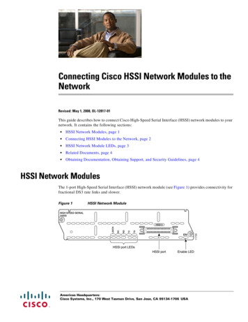
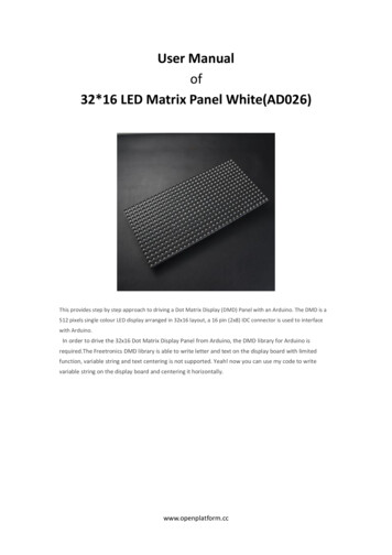
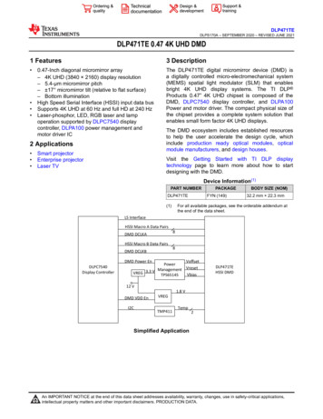
DLP471TEDLPS170A – SEPTEMBER 2020 – REVISED JUNE 2021DLP471TE 0.47 4K UHD DMD1 Features3 Description The DLP471TE digital micromirror device (DMD) isa digitally controlled micro-electromechanical system(MEMS) spatial light modulator (SLM) that enablesbright 4K UHD display systems. The TI DLP Products 0.47” 4K UHD chipset is composed of theDMD, DLPC7540 display controller, and DLPA100Power and motor driver. The compact physical size ofthe chipset provides a complete system solution thatenables small form factor 4K UHD displays. 0.47-Inch diagonal micromirror array– 4K UHD (3840 2160) display resolution– 5.4-µm micromirror pitch– 17 micromirror tilt (relative to flat surface)– Bottom illuminationHigh Speed Serial Interface (HSSI) input data busSupports 4K UHD at 60 Hz and full HD at 240 HzLaser-phosphor, LED, RGB laser and lampoperation supported by DLPC7540 displaycontroller, DLPA100 power management andmotor driver IC2 Applications Smart projectorEnterprise projectorLaser TVThe DMD ecosystem includes established resourcesto help the user accelerate the design cycle, whichinclude production ready optical modules, opticalmodule manufacturers, and design houses.Visit the Getting Started with TI DLP displaytechnology page to learn more about how to startdesigning with the DMD.Device Information(1)PART NUMBERDLP471TE(1)PACKAGEFYN (149)BODY SIZE (NOM)32.2 mm 22.3 mmFor all available packages, see the orderable addendum atthe end of the data sheet.LS InterfaceHSSI Macro A Data Pairs8DMD DCLKAHSSI Macro B Data Pairs8DMD DCLKBDMD Power EnDLPC7540Display ControllerVoffsetPowerManagement VresetVREG 3.3 V TPS65145VbiasDLP471TEHSSI DMD12 V1.8 VDMD VDD EnI2CVREGTMP411Temp2Simplified ApplicationAn IMPORTANT NOTICE at the end of this data sheet addresses availability, warranty, changes, use in safety-critical applications,intellectual property matters and other important disclaimers. PRODUCTION DATA.
DLP471TEwww.ti.comDLPS170A – SEPTEMBER 2020 – REVISED JUNE 2021Table of Contents1 Features.12 Applications. 13 Description.14 Revision History. 25 Pin Configuration and Functions.36 Specifications. 66.1 Absolute Maximum Ratings. 66.2 Storage Conditions. 76.3 ESD Ratings. 76.4 Recommended Operating Conditions.76.5 Thermal Information.96.6 Electrical Characteristics.96.7 Switching Characteristics. 116.8 Timing Requirements. 126.9 System Mounting Interface Loads. 166.10 Micromirror Array Physical Characteristics. 176.11 Micromirror Array Optical Characteristics. 186.12 Window Characteristics. 206.13 Chipset Component Usage Specification. 207 Detailed Description.217.1 Overview. 217.2 Functional Block Diagram. 217.3 Feature Description.227.4 Device Functional Modes.227.5 Optical Interface and System Image QualityConsiderations. 227.6 Micromirror Array Temperature Calculation. 237.7 Micromirror Landed-On/Landed-Off Duty Cycle. 258 Application and Implementation. 288.1 Application Information. 288.2 Typical Application. 288.3 Temperature Sensor Diode. 319 Power Supply Recommendations.339.1 DMD Power Supply Power-Up Procedure. 339.2 DMD Power Supply Power-Down Procedure. 3310 Layout.3510.1 Layout Guidelines. 3510.2 Impedance Requirements.3510.3 Layers. 3510.4 Trace Width, Spacing.3610.5 Power.3610.6 Trace Length Matching Recommendations. 3711 Device and Documentation Support.3811.1 Device Support.3811.2 Documentation Support. 3911.3 Receiving Notification of Documentation Updates. 3911.4 Support Resources. 3911.5 Trademarks. 3911.6 Electrostatic Discharge Caution. 3911.7 Glossary. 3912 Mechanical, Packaging, and OrderableInformation. 4012.1 Package Option Addendum. 414 Revision HistoryNOTE: Page numbers for previous revisions may differ from page numbers in the current version.Changes from Revision * (September 2020) to Revision A (June 2021)Page Updated minimum value of VID CLK Section 6.4 . 7 Updated ILLUV value and wavelength range in Section 6.4 .7 Updated table header with package information in Section 6.5 .9 Corrected typo in Figure 6-8 . 12 Update table in Section 6.12 .20 Corrected typo in Section 7.2 . 21 Corrected typo in Section 7.7.4. 25 Added pin connection conditions for when the temp sensor is not used in Section 8.3. . 31 Merged Table 9-1 and Table 9-2 into a new Table 9-1 .33 Updated table references to reflect Table 9-2 was merged into Table 9-1 in Section 9.1 .33 Updated table references to reflect Table 9-2 was merged into Table 9-1 and fixed typos in Section 9.2 .33 Updated Figure 9-1 .332Submit Document FeedbackCopyright 2021 Texas Instruments IncorporatedProduct Folder Links: DLP471TE
DLP471TEwww.ti.comDLPS170A – SEPTEMBER 2020 – REVISED JUNE 20215 Pin Configuration and Functions132547698111013 15 17 1912 14 16 18 20TRPNMLKJHGFEDCBAFigure 5-1. FYN Package 149-Pin PGA Bottom ViewCAUTIONProperly manage the layout and the operation of signals identified in the Pin Functions table to make sure there is reliable,long-term operation of the .47” 4K UHD S451 DMD. Refer to the PCB Design Requirements for TI DLP TRP DigitalMicromirror Devices application report for specific details and guidelines before designing the board.Table 5-1. Pin LENGTH (mm)D AP(0)J1IHigh–speed Diffierential Data Pair lane A016.24427D AN(0)H1IHigh–speed Diffierential Data Pair lane A016.24426D AP(1)G1IHigh–speed Diffierential Data Pair lane A116.39699D AN(1)F1IHigh–speed Diffierential Data Pair lane A116.39691D AP(2)F2IHigh–speed Diffierential Data Pair lane A215.58905D AN(2)E2IHigh–speed Diffierential Data Pair lane A215.58908D AP(3)D2IHigh–speed Diffierential Data Pair lane A314.98471D AN(3)C2IHigh–speed Diffierential Data Pair lane A314.9844D AP(4)A3IHigh–speed Diffierential Data Pair lane A412.89101D AN(4)A4IHigh–speed Diffierential Data Pair lane A412.89101D AP(5)A5IHigh–speed Diffierential Data Pair lane A510.57206D AN(5)A6IHigh–speed Diffierential Data Pair lane A510.57242D AP(6)A7IHigh–speed Diffierential Data Pair lane A68.48593D AN(6)A8IHigh–speed Diffierential Data Pair lane A68.48702D AP(7)A9IHigh–speed Diffierential Data Pair lane A76.63434D AN(7)A10IHigh–speed Diffierential Data Pair lane A76.63441Submit Document FeedbackCopyright 2021 Texas Instruments IncorporatedProduct Folder Links: DLP471TE3
DLP471TEwww.ti.comDLPS170A – SEPTEMBER 2020 – REVISED JUNE 2021Table 5-1. Pin Functions (continued)PINNAME4INPUT-OUTPUT(1)No.TRACELENGTH (mm)DESCRIPTIONDCLK APC1IHigh–speed Diffierential Clock A15.53899DCLK AND1IHigh–speed Diffierential Clock A15.53868D BP(0)A11IHigh–speed Diffierential Data Pair lane B04.52398D BN(0)A12IHigh–speed Diffierential Data Pair lane B04.52368D BP(1)A13IHigh–speed Diffierential Data Pair lane B16.4103D BN(1)A14IHigh–speed Diffierential Data Pair lane B16.40894D BP(2)A15IHigh–speed Diffierential Data Pair lane B28.78102D BN(2)A16IHigh–speed Diffierential Data Pair lane B28.78364D BP(3)A18IHigh–speed Diffierential Data Pair lane B312.05827D BN(3)A19IHigh–speed Diffierential Data Pair lane B312.06154D BP(4)D19IHigh–speed Diffierential Data Pair lane B411.04817D BN(4)C19IHigh–speed Diffierential Data Pair lane B411.0479D BP(5)H20IHigh–speed Diffierential Data Pair lane B514.54976D BN(5)J20IHigh–speed Diffierential Data Pair lane B514.54991D BP(6)D20IHigh–speed Diffierential Data Pair lane B611.67363D BN(6)E20IHigh–speed Diffierential Data Pair lane B611.67598D BP(7)F20IHigh–speed Diffierential Data Pair lane B712.33442D BN(7)G20IHigh–speed Diffierential Data Pair lane B712.33409DCLK BPB17IHigh–speed Diffierential Clock B10.22973DCLK BNB18IHigh–speed Diffierential Clock B10.22551LS WDATA PT10ILVDS Data7.8047LS WDATA NR11ILVDS Data0.64391LS CLK PR9ILVDS CLK8.20952LS CLK NR10ILVDS CLK7.35885LS RDATA A BT13ISTAOLVCMOS Output2.01174BIST BT12OLVCMOS Output2.20006AMUX OUTB20OAnalog Test Mux10.74435DMUX OUTR14ODigital Test Mux2.25459DMD DEN ARSTZT11IARSTZ2.00365TEMP NR8ITemp Diode N9.03231TEMP PR7ITemp Diode P11.38391VDDB13, B7, C18,E3, H3, J2, K3,L2, L19, M1, M2,N3, N19, P2,PP18, R3, R5,R12, R17, R19,T2, T4, T6, T8,T18Digital Core Supply VoltagePlaneVDDAB11, B16, B4,B9, C20, D3,E18, G2, G19PHSSI Supply VoltagePlaneVRESETB3, R1PSupply Voltage for Negative Bias of Micromirror reset signalPlaneVBIASE1, P1PSupply Voltage for Positive Bias of Micromirror reset signalPlaneVOFFSETA20, B2, T1,T20PSupply voltage for HVCMOS logic,stepped up logic levelPlaneSubmit Document FeedbackCopyright 2021 Texas Instruments IncorporatedProduct Folder Links: DLP471TE
DLP471TEwww.ti.comDLPS170A – SEPTEMBER 2020 – REVISED JUNE 2021Table 5-1. Pin Functions CELENGTH (mm)VSSA17, B10, B14,B6, D18, F3,F19, J3, K19,K2, L1, L3, M3,N2, N18, N20,GP3, P20, R2, R4,R6, R13, R20,T5, T7, T16,T17, T19GroundPlaneVSSAB12, B15, B19,B5, B8, C3, E19,G3, H2, H19,GK1, N1, P19,R18, T3, T9GroundPlaneN/CF18, G18, H18,J18, J19, K18,K20, L18, L20,M18, M19, M20,R15, R16, T14,T15No Connect(1)I Input, O Output, P Power, G Ground, NC No ConnectSubmit Document FeedbackCopyright 2021 Texas Instruments IncorporatedProduct Folder Links: DLP471TE5
DLP471TEwww.ti.comDLPS170A – SEPTEMBER 2020 – REVISED JUNE 20216 Specifications6.1 Absolute Maximum RatingsStresses beyond those listed under Absolute Maximum Ratings may cause permanent damage to the device. These arestress ratings only, and functional operation of the device is not implied at these or any other conditions beyond thoseindicated under Recommended Operating Conditions. Exposure above or below the Recommended Operating Conditions forextended periods may affect device reliability.MINMAXUNITSUPPLY VOLTAGEVDDSupply voltage for LVCMOS core logic and LVCMOS low speed interface(LSIF)(1)–0.52.3VVDDASupply voltage for high speed serial interface (HSSI) receivers(1)–0.32.2VVOFFSETSupply voltage for HVCMOS and micromirror electrode(1) (2)–0.511VVBIASSupply voltage for micromirrorelectrode(1)–0.519VVRESETSupply voltage for micromirror electrode(1)–150.5V VDDA – VDD Supply voltage delta (absolutevalue)(3)0.3V VBIAS – VOFFSET Supply voltage delta (absolute value)(4)11Vvalue)(5)34V–0.52.45V–0.2VDDAV VBIAS – VRESET Supply voltage delta (absoluteINPUT VOLTAGEInput voltage for other inputs – LSIF and LVCMOS(1)Input voltage for other inputs –HSSI(1) (6)LOW SPEED INTERFACE (LSIF)fCLOCKLSIF clock frequency (LS CLK)130MHz VID LSIF differential input voltage magnitude(6)810mVIIDLSIF differential input current10mAHIGH SPEED SERIAL INTERFACE (HSSI)fCLOCKHSSI clock frequency (DCLK)1.65GHz VID HSSI differential input voltage magnitude Data Lane(6)700mV700mV090 C–4090 C VID HSSI differential input voltage magnitude ClockLane(6)ENVIRONMENTALTWINDOW and TARRAYTemperature, non-operating(7) TDELTA Absolute temperature delta between any point on the window edge and theceramic test point TP1(8)30 CTDPDew point temperature, operating and non–operating (noncondensing)81 C(1)(2)(3)(4)(5)(6)(7)(8)6Temperature, operating(7)All voltage values are with respect to the ground terminals (VSS). The following required power supplies must be connected for properDMD operation: VDD, VDDA, VOFFSET, VBIAS, and VRESET. All VSS connections are also required.VOFFSET supply transients must fall within specified voltages.Exceeding the recommended allowable absolute voltage difference between VDDA and VDD may result in excessive current draw.Exceeding the recommended allowable absolute voltage difference between VBIAS and VOFFSET may result in excessive current draw.Exceeding the recommended allowable absolute voltage difference between VBIAS and VRESET may result in excessive current draw.This maximum input voltage rating applies when each input of a differential pair is at the same voltage potential. LVDS and HSSIdifferential inputs must not exceed the specified limit or damage may result to the internal termination resistors.The highest temperature of the active array (as calculated using Micromirror Array Temperature Calculation) or of any point along thewindow edge as defined in Figure 7-1. The locations of thermal test points TP2, TP3, TP4 and TP5 in Figure 7-1 are intended tomeasure the highest window edge temperature. If a particular application causes another point on the window edge to be at a highertemperature, that point should be used.Temperature delta is the highest difference between the ceramic test point 1 (TP1) and anywhere on the window edge as shown inFigure 7-1. The window test points TP2, TP3, TP4, and TP5 shown in Figure 7-1 are intended to result in the worst case delta. If aparticular application causes another point on the window edge to result in a larger delta temperature, that point should be used.Submit Document FeedbackCopyright 2021 Texas Instruments IncorporatedProduct Folder Links: DLP471TE
DLP471TEwww.ti.comDLPS170A – SEPTEMBER 2020 – REVISED JUNE 20216.2 Storage ConditionsApplicable for the DMD as a component or non-operating in a system.TDMDDMD temperatureTDP-AVGAverage dew point temperature, non-condensing(1)non-condensing(2)TDP-ELRElevated dew point temperature range,CTELRCumulative time in elevated dew point temperature range(1)(2)MINMAX–4080 C28 C28UNIT36 C24monthsThe average temperature over time (including storage and operating temperatures) that the device is not in the elevated dew pointtemperature range.Exposure to dew point temperatures in the elevated range during storage and operation should be limited to less than a totalcumulative time of CTELR.6.3 ESD RatingsV(ESD)(1)(2)ElectrostaticdischargeHuman body model (HBM), per ANSI/ESDA/JEDEC JS-001(1)Charged device model (CDM), per JEDEC specificationVALUEUNIT 2000V 500VJESD22-C101(2)JEDEC document JEP155 states that 500 V HBM allows safe manufacturing with a standard ESD control process.JEDEC document JEP157 states that 250 V CDM allows safe manufacturing with a standard ESD control process.6.4 Recommended Operating #GUID-DB050334-17E7-422B-91B0-D62FF359059DOver operating free-air temperature range and supply voltages (unless otherwise noted). The functional performance of thedevice specified in this data sheet is achieved when operating the device within the limits defined by the RecommendedOperating Conditions. No level of performance is implied when operating the device above or below the RecommendedOperating Conditions limits.SUPPLY VOLTAGESMINTYPMAXUNIT(1) (2)VDDSupply voltage for LVCMOS core logic and low speedinterface (LSIF)1.711.81.95VVDDASupply voltage for high speed serial interface (HSSI) receivers1.711.81.95Velectrode(3)VOFFSETSupply voltage for HVCMOS and micromirror9.51010.5VVBIASSupply voltage for micromirror electrode17.51818.5VVRESETSupply voltage for micromirror electrode–14.5–14–13.5V VDDA – VDD Supply voltage delta, absolute value(4)0.3Vvalue(5)10.5V33V VBIAS – VOFFSET Supply voltage delta, absolute VBIAS – VRESET Supply voltage delta, absolute valueLVCMOS INPUTVIHHigh level input voltage(6)VILvoltage(6)Low level input0.7 x VDDV0.3 x VDDVLOW SPEED SERIAL INTERFACE (LSIF)fCLOCKLSIF clock frequency (LS CLK)(7)DCDINLSIF duty cycle distortion (LS CLK) VID LSIF differential input voltageVLVDSLSIF 30MHz56%440mV1520mVmVVCMCommon mode7009001300ZLINELine differential impedance (PWB/trace)90100110ΩZINInternal differential termination resistance80100120Ω1.6GHzHIGH SPEED SERIAL INTERFACE (HSSI)fCLOCKHSSI clock frequency (DCLK)(8)1.2Submit Document FeedbackCopyright 2021 Texas Instruments IncorporatedProduct Folder Links: DLP471TE7
DLP471TEwww.ti.comDLPS170A – SEPTEMBER 2020 – REVISED JUNE 2021Over operating free-air temperature range and supply voltages (unless otherwise noted). The functional performance of thedevice specified in this data sheet is achieved when operating the device within the limits defined by the RecommendedOperating Conditions. No level of performance is implied when operating the device above or below the RecommendedOperating Conditions limits.DCDINHSSI duty cycle distortion (DCLK)Lane(8) VID DataHSSI differential input voltage magnitude Data VID CLKHSSI differential input voltage magnitude Clock C DataInput common mode voltage (DC) DataVCMDC CLKInput common mode voltage (DC) Clk Lane(8)VCMACp-pAC peak to peak (ripple) on common mode voltage of DataLane and Clock Lane(8)ZLINELine differential impedance (PWB/trace)ZINInternal differential termination resistance. ( RXterm )80Array temperature, long–term operational(9) (10) (11) (12) 40 to 70 C010 CENVIRONMENTALTARRAYArray temperature, short-term operational, 500 hr max(10) (14)operational(15)TWINDOWWindow temperature,85 C TDELTA Absolute temperature delta between any point on the windowedge and the ceramic test point TP1(16)14 CTDP-AVGAverage dew point temperature (non–condensing)(17)28 C(non-condensing)(18)TDP-ELRElevated dew point temperature range36 CCTELRCumulative time in elevated dew point temperature range2824monthsILLθIllumination marginal ray angle(19)55degrees2mW/cm2LAMP ILLUMINATIONILLUVIllumination wavelength 395 nm(9)ILLVISIllumination wavelengths between 395 nm and 800 nm(13)ILLIRIllumination wavelength 800 nm0.6836.8W/cm210mW/cm23mW/cm2SOLID STATE ILLUMINATIONIllumination wavelength 410 nm(9)ILLUVILLVISIllumination wavelengths between 410 nm and 800ILLIRIllumination wavelength 800 15)8nm(13)44.910W/cm2mW/cm2All power supply connections are required to operate the DMD: VDD, VDDA, VOFFSET, VBIAS, and VRESET. All VSS connections arerequired to operate the DMD.All voltage values are with respect to the VSS ground pins.VOFFSET supply transients must fall within specified max voltages.To prevent excess current, the supply voltage delta VDDA – VDD must be less than specified limit.To prevent excess current, the supply voltage delta VBIAS – VOFFSET must be less than specified limit.LVCMOS input pin is DMD DEN ARSTZ.See the low speed interface (LSIF) timing requirements in Timing Requirements.See the high speed serial interface (HSSI) timing requirements in Timing Requirements.Simultaneous exposure of the DMD to the maximum Recommended Operating Conditions for temperature and UV illuminationreduces device lifetime.The array temperature cannot be measured directly and must be computed analytically from the temperature measured at test point(TP1) shown in Figure 7-1 and the package thermal resistance using the Micromirror Array Temperature Calculation.Per Figure 6-1, the maximum operational array temperature should be derated based on the micromirror landed duty cycle that theDMD experiences in the end application. Refer to Micromirror Landed-On/Landed-Off Duty Cycle for a definition of micromirror landedduty cycle.Long-term is defined as the usable life of the device.The maximum optical power that can be incident on the DMD is limited by the maximum optical power density and the micromirrorarray temperatureShort-term is the total cumulative time over the useful life of the device.The locations of thermal test points TP2, TP3, TP4, and TP5 shown in Figure 7-1 are intended to measure the highest window edgetemperature. For most applications, the locations shown are representative of the highest window edge temperature. If a particularapplication causes additional points on the window edge to be at a higher temperature, test points should be added to those locations.Submit Document FeedbackCopyright 2021 Texas Instruments IncorporatedProduct Folder Links: DLP471TE
DLP471TEwww.ti.comDLPS170A – SEPTEMBER 2020 – REVISED JUNE 2021Maximum Recommended Array Temperature - Operational (¹C)(16) Temperature delta is the highest difference between the ceramic test point 1 (TP1) and anywhere on the window edge as shownin Figure 7-1. The window test points TP2, TP3, TP4, and TP5 shown in Figure 7-1 are intended to result in the worst case deltatemperature. If a particular application causes another point on the window edge to result in a larger delta in temperature, that pointshould be used.(17) The average over time (including storage and operating) that the device is not in the ‘elevated dew point temperature range'.(18) Exposure to dew point temperatures in the elevated range during storage and operation should be limited to less than a totalcumulative time of CTELR.(19) The maximum marginal ray angle of the incoming illumination light at any point in the micromirror array, including pond of micromirrors(POM), should not exceed 55 degrees from the normal to the device array plane. The device window aperture has not necessarilybeen designed to allow incoming light at higher maximum angles to pass to the micromirrors, and the device performance has notbeen tested nor qualified at angles exceeding this. Illumination light exceeding this angle outside the micromirror array (including POM)will contribute to thermal limitations described in this document, and may negatively affect 30/7035/6540/6045/55 5/4550/50Micromirror Landed Duty CycleFigure 6-1. Maximum Recommended Array Temperature - Derating Curve6.5 Thermal InformationDLP471TETHERMAL METRICFYN PACKAGEUnit149 PINSThermal Resistance, active area to test point 1 (TP1)(1)(1)0.8 C/WThe DMD is designed to conduct absorbed and dissipated heat to the back of the package. The cooling system must be capable ofmaintaining the DMD within the temperature range specified in the Section 6.4. The total heat load on the DMD is largely driven bythe incident light absorbed by the active area; although other contributions include light energy absorbed by the window aperture andelectrical power dissipation of the array. Optical systems should be designed to minimize the light energy falling outside the windowclear aperture since any additional thermal load in this area can significantly degrade the reliability of the device.6.6 Electrical CharacteristicsOver operating free-air temperature range and supply voltages (unless otherwise noted)PARAMETER (1) (2)TEST CONDITIONS (1)MINTYPMAX UNITCURRENT – TYPICALIDDSupply current VDD (3)8001200mAIDDASupply current VDDA (3)10001200mAIDDASupply current VDDA(3)500600mAIOFFSETSupply current VOFFSET (4) (5)2025mASingle macro modeSubmit Document FeedbackCopyright 2021 Texas Instruments IncorporatedProduct Folder Links: DLP471TE9
DLP471TEwww.ti.comDLPS170A – SEPTEMBER 2020 – REVISED JUNE 2021Over operating free-air temperature range and supply voltages (unless otherwise noted)PARAMETER (1) (2)IBIASSupply current VBIASIRESETTEST CONDITIONS (1)MIN(4) (5)Supply current VRESETTYP2.5(5)-9.3MAX UNIT4.0-6.9mAmAPOWER – TYPICALPDDSupply power dissipation VDD (3)14402437.5mWPDDASupply power dissipation VDDA (3)16202340mWPDDASupply power dissipation VDDA 367.55mWsingle macro mode(4) (5)POFFSETSupply power dissipation VOFFSETPBIASSupply power dissipation VBIAS (4) (5)PRESETSupply power dissipation VRESETPTOTALSupply power dissipation Total(5)LVCMOS INPUTIILLow level input current (6)IIH(6)High level input currentVDD 1.95 V, VI 0 V–100VDD 1.95 V, VI 1.95 VnA135uALVCMOS OUTPUTVOHDC output high voltage (7)IOH -2 mAVOLDC output low voltage (7)IOL 2 mA0.8 x VDDV0.2 x VDDVRECEIVER EYE CHARACTERISTICSMinimum data eye opening (8) (9)100600mV295600mV600mVX1Maximum data eye closure(8)0.275UIX2Maximum data eye closure (8)0.4UI tDRIFT Drift between Clock and Data betweenTraining Patterns20psA1Minimum clock eye opening(8) (9)Maximum data signal swing (8) (9)A2CAPACITANCECINInput capacitance LVCMOSf 1 MHz10pFCINInput capacitance LSIF (low speedinterface)f 1 MHz20pFCINInput capacitance HSSI (high speed serialf 1 MHzinterface)20pFCOUTOutput capacitance10pF(1)(2)(3)(4)(5)(6)(7)(8)(9)10f 1 MHzAll power supply connections are required to operate the DMD: VDD, VDDA, VOFFSET, VBIAS, and VRESET. All VSS connections arerequired to operate the DMD.All voltage values are with respect to the ground pins (VSS).To prevent excess current, the supply voltage delta VDDA – VDD must be less than specified limit.To prevent excess current, the supply voltage delta VBIAS – VOFFSET must be less than specified limit.Supply power dissipation based on 3 global resets in 200 µs.LVCMOS input specifications are for pin DMD DEN ARSTZ.LVCMOS output specification is for pins LS RDATA A and LS RDATA B.Refer to Figure 6-11, Receiver Eye Mask (1e-12 BER).Defined in Recommended Operating Conditions.Submit Document FeedbackCopyright 2021 Texas Instruments IncorporatedProduct Folder Links: DLP471TE
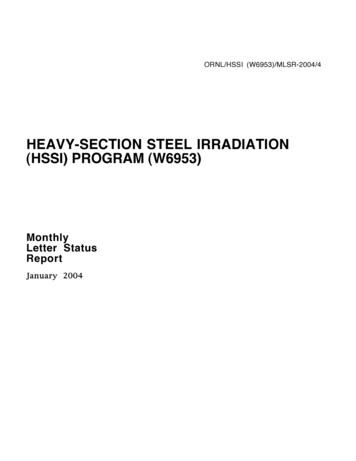
DLP471TEwww.ti.comDLPS170A – SEPTEMBER 2020 – REVISED JUNE 20216.7 Switching CharacteristicsOver operating free-air temperature range and supply voltages (unless otherwise noted)PARAMETERtpd(1)TEST CONDITIONSMINTYPMAXUNITOutput propagation, Clock to Q (C2Q), rising edge ofLS CLK (differential clock signal) input to LS RDATAoutput.(1)CL 5 pF11.1nsCL 10 pF11.3nsSlew rate, LS RDATA20%-80%, CL 10pF0.5Output duty cycle distortion, LS RDATA A andLS RDATA B50-(C2Q rise - C2Qfall )*130e6*10040V/ns60%See Figure 6-2LS CLK P1010011010LS CLK N1 periodLS WDATA PStop (1)Start (0)LS WDATA NtPDLS RDATA ABIST AAcknowledgeFigure 6-2. Switching CharacteristicsSubmit Document FeedbackCopyright 2021 Texas Instruments IncorporatedProduct Folder Links: DLP471TE11
DLP471TEwww.ti.comDLPS170A – SEPTEMBER 2020 – REVISED JUNE 20216.8 Timing RequirementsOver operating free-air temperature range and supply voltages (unless otherwise noted)PARAMETERTEST CONDITIONSMINTYPMAXUNITLVCMOSRise time(1)trtfFalltime(1)20% to 80% reference points25ns80% to 20% reference points25nsLOW SPEED INTERFACE (LSIF)trRise time(2)20% to 80% reference points450pstfFall time(2)80% to 20% reference points450pshigh(3)tW(H)Pulse durationLS CLK. 50% to 50% reference points3.1nstW(L)Pulse duration low(3)LS CLK. 50% to 50% reference points3.1nstsuSetup time(4)LS WDATA valid before rising edge of LS CLK(differential)1.5nsthHold time(4)LS WDATA valid after rising edge of LS CLK(differential)1.5nsHIGH SPEED SERIAL INTERFACE (HSSI)trRise time(5) (6) - datafrom -A1 to A1 minimum eye height specification50115psRise time(5) (6) - clockrom -A1 to A1 minimum eye height specification50135pspsFalltime(5) (6)from A1 to -A1 minimum eye height specification50115Fall time(5) (6) - clockfrom A1 to -A1 minimum eye height specification50135tW(H)Pulse duration high(7)DCLK. 50% to 50% reference points0.275nstW(L)Pulse duration low(7)DCLK. 50% to 50% reference points0.275nstf(1)(2)(3)(4)(5)(6)(7)- dataSee Figure 6-9 for rise time and fall time for LVCMOS.See Figure 6-5 for rise time and fall time for LSIF.See Figure
HSSI Maco Ar Data Paisr HSSI Maco r B Data Paisr DMD DCLKA DMD DCLKB 8 8 P roew Managnteme TPS65145 Votffse Vtseer Vbias VREG 1.8 V TMP411 Tpm e 2 I2C DMD P roew En DMD VDD En 12 V DLPC7540 Display Coonlrtlre VREG 3.3 V Simplified Application www.ti.com DLP471TE DLPS170 - SEPTEMBER 2020