Transcription
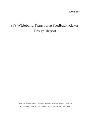
DATA SHEETSKY73134-11: Wideband PLL Frequency SynthesizerApplicationsDescription Cellular base station systems: GSM/EDGE, CDMA2000, WCDMA,TD-SCDMA, LTEThe SKY73134-11 is a wideband integer-N frequency synthesizerwith an approximately 6 GHz locking range. Other wireless communication systemsThe device includes four differential Voltage Controlled Oscillators(VCOs), which cover the output frequency range from 2.8 GHz to6.2 GHz. By applying internal VCO division by 1, 2, 3, 4, or 8, theoutput frequency range can be increased from 0.35 GHz to6.2 GHz, monitored at the RF output.Features Continuous frequency coverage: 0.35 to 6.2 GHz Integer-N frequency synthesizer Low phase noise VCO Four integrated VCOs with automatic digital frequencycalibration Automatic VCO selection based on the target RF output Programmable VCO division by 1, 2, 3, 4, or 8 VCO divide-by-three with 50% duty cycle Integrated input/output RF buffer Device provides both divided and direct VCO outputs Programmable RF output power levelsThe direct, non-divided internal VCO frequency can also bemonitored at the bidirectional VCO pins. The VCO selection can beautomatic based on the target RF output. The flexibleSKY73134-11 configuration allows the loop to be locked by anexternal VCO or external Phase Locked Loop (PLL), or the devicecan use the divider chain only. The SKY73134-11 is controlled bya bidirectional read/write serial to parallel interface.The SKY73134-11 frequency synthesizer is manufactured with aBiCMOS 0.18 μm SiGe process and provided in a compact,32-pin RF Land Grid Array (RFLGA). The pin configuration andpackage are shown in Figure 1. A functional block diagram isshown in Figure 2. Signal pin assignments and functional pindescriptions are provided in Table 1. Low RF output comparison spurs Small, RFLGA (32-pin, 5 x 5 mm) package (MSL3, 260 C perJEDEC J-STD-020)Skyworks Pb-free products are compliant withall applicable legislation. For additionalinformation, refer to Skyworks Definition ofLead (Pb)-Free, document number SQ04-0073.N/CN/CN/CN/CN/C2625 CLKVCC CAP224 DATAVCO RES323 LEOUT BUFP422 EXT VCONOUT BUFN521 EXT VCOPVCC OBUF620 PLL RESDIV CAP719 REF CLKDIV RES818 GND REFVCC DIV917 VCC REF10111213141516VCC DIG Power supply: 3.3 V27LD OUT Optional adjustment of the core, divider, and charge pumpcurrent by external resistor28LF CTRL Digital output used as a loop filter component switch29CP OUT Digital lock detect30VCO CP Bidirectional read/write three-wire serial to parallel interface311VCTRL Flexible configuration allows connection to external VCO or PLL32VCC VCOVCC PLL Programmable charge pump currentN/C Dual modulus 7 GHz prescaler (selectable 16/17 or 32/33)N/C Programmable 18-bit N-counter and 11-bit R-counterS1839Figure 1. SKY73134-11 Pinout – 32-Pin RFLGA(Top View)Skyworks Solutions, Inc. Phone [781] 376-3000 Fax [781] 376-3100 sales@skyworksinc.com www.skyworksinc.com201199F Skyworks Proprietary Information Products and Product Information are Subject to Change Without Notice December 14, 20111
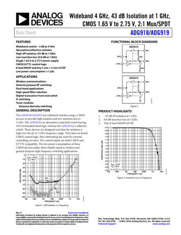
DATA SHEET SKY73134-11 FREQUENCY SYNTHESIZERCLKVCO1VCO2VCO3VCO4Read/WriteSPIDATALE 1 2OutputBufferOUT BUFPOUT BUFNVCOOutVCOBufferEXT VCONEXT VCOP 3 4PLLBufferVCOIn 8N-DividerR-DividerREF CLKRefBufferDigital Frequency ControlVCO CalibrationCharge PumpLock DetectCP OUTLD OUTVCTRLPhase DetectorS1838Figure 2. SKY73134-11 Block DiagramTable 1. SKY73134-11 Signal DescriptionsPin #NameDescriptionPin #NameDescription1VCC VCOSupply for VCO17VCC REFSupply for reference buffer2VCC CAPExternal capacitor for VCO bias connectedto VCC VCO pin18GND REFReference buffer ground3VCO RESExternal 15 kΩ resistor to set VCO bias19REF CLKReference clock input4OUT BUFPPositive LO output20PLL RESExternal 20 kΩ resistor for the PLL/chargepump bias5OUT BUFNNegative LO output21EXT VCOPPositive, external VCO input6VCC OBUFSupply for output buffer22EXT VCONNegative, external VCO input7DIV CAPExternal capacitor for the divider biasconnected to the VCC DIV pin23LELatch enable input for the SPI8DIV RESExternal 60 kΩ resistor to set the dividerbias24DATAData input for the SPI9VCC DIVSupply for dividers25CLKClock input for the SPI10VCTRLVCO tuning voltage26N/CNo connection11VCC PLLPLL supply27N/CNo connection12VCC CPSupply for charge pump28N/CNo connection13CP OUTCharge pump output29N/CNo connection14LF CTRLLoop filter component switch control30N/CNo connection15LD OUTLock detect output31N/CNo connection16VCC DIGSupply for digital blocks32N/CNo connectionSkyworks Solutions, Inc. Phone [781] 376-3000 Fax [781] 376-3100 sales@skyworksinc.com www.skyworksinc.com2December 14, 2011 Skyworks Proprietary Information Products and Product Information are Subject to Change Without Notice 201199F
DATA SHEET SKY73134-11 FREQUENCY SYNTHESIZERFunctional DescriptionCharge PumpThe SKY73134-11 is comprised of seven main functional blocks:The charge pump is used to convert the logic levels of the Up andDn pulses, carrying the phase error between the reference andthe divided signal into analog quantities/current pulses.1. N-divider2. R-divider3. Phase detector4. Charge pump5. VCO and digital frequency VCO calibration6. VCO dividersThe output of the SKY73134-11 charge pump is programmableand varies between 0.9 mA and 5.4 mA. Additional adjustment ofthe charge pump current can be accomplished by changing thevalue of the external PLL bias resistor.VCO and Digital Frequency VCO Calibration7. Lock detectThe SKY73134-11 incorporates four VCOs. Each VCO covers adifferent frequency range between 2.8 and 6.2 GHz.N-DividerThe N-divider consists of a selectable 16/17 or 32/33 prescaler,13-bit main counter, and 5-bit swallow counter. The 18-bit Ndivider ratio is calculated as:N P M SWhere: P Prescaler valueM Main counter valueS Swallow counter valueThe N-divider range is from P2 to 218. For a 32/33 prescaler, theN-divider range varies from 1024 to 262144.R-DividerThe 11-bit programmable R-divider divides the reference inputfrequency and generates the reference input for the phasedetector. The R-divider range varies from 1 to 211 (2048).Phase DetectorThe phase detector is an edge-controlled digital circuit. Thecircuit has two inputs: the reference signal (Ref) and the N-divideroutput. There are two digital outputs (Up and Dn) that drive thecharge pump.When the input phase difference is positive, the Up output ispulled up to VDD. When the input phase difference is negative,the Dn output is pulled down to ground. This type of phasedetector acts only on the positive edges of the input signals.The VCOs are designed to generate the LO signal with the tuningfunction controlled by the synthesizer. Each VCO uses a switchcapacitor array and an analog varactor for digital tuning. Thedigital auto-tuning loop provides the proper coarse tuning settingfor the VCO switch capacitors. This sets the oscillation frequencyas close to target as possible before starting fine analog tuning.When VCO auto-tuning is enabled, the PLL performs a successiveapproximation process to digitally tune the VCO close to the finalprogrammed frequency. Once that is complete, analog tuning isenabled to lock the VCO to the programmed frequency.The auto-tuning loop is designed to compensate process variationso that the VCO fine tuning range can be reduced to covertemperature variation only. This ensures that the PLL is alwayslocked.VCO DividersThe divider chain consists of dividers and LO drivers. Any VCO canbe divided by 2, 3, 4, or 8, which improves the LO phase noise by6 dB, 9.5 dB, 12 dB, and 18 dB, respectively.Using frequency division, the overall VCO range of the device iswidened from 0.35 to 6.2 GHz.The output RF buffer has a programmable current that providesvariation in the output RF level. The direct non-divided VCO outputcan be monitored at the additional bidirectional internal/externalVCO pins. The divider chain and the internal PLL can be locked byan external VCO.Skyworks Solutions, Inc. Phone [781] 376-3000 Fax [781] 376-3100 sales@skyworksinc.com www.skyworksinc.com201199F Skyworks Proprietary Information Products and Product Information are Subject to Change Without Notice December 14, 20113
DATA SHEET SKY73134-11 FREQUENCY SYNTHESIZERcycle is inserted so the baseband can disable its drive of the dataline and the addressed device on the bus can activate its dataoutput driver.Lock DetectThe lock detect circuit is activated when the phase differencebetween the Up and Dn phase detector signals for a given numberof comparison cycles is shorter than a fixed delay. The CMOSoutput is active high when the loop is locked.When the baseband addresses a device connected to the serialbus, the bus enable signal (LE) goes low half a clock cycle beforethe CLK signal becomes active. Data on the DATA line is clockedinto the SKY73134-11 on the rising edge of the clock.Bidirectional Digital InterfaceData from the SKY73134-11 to the baseband is clocked at thefalling edge of the clock. The enable line goes high at the end ofthe data transfer.A three-wire Serial Programmable Interface (SPI) with read/writecapability provides mode and bias control, and control of the PLL.The serial interface consists of three signals: the bus clock (CLK),latch enable (LE), and the serial, bidirectional data line (DATA).A timing diagram for the SPI read/write cycle is shown inFigure 3.Write Mode. A write data stream consists of 25 bits:Bits[15:0] provide the 16-bit data block.Serial Bus TimingBits[20:16] provide the register address.The SPI bus speed is programmable. Timing requirements for theCLK, DATA, and LE signals are provided in Table 2. A serial datainput timing diagram is shown in Figure 4.Bit[21] is the read/write bit (0 read, 1 write).Bits[24:22] provide the device address (the SKY73134-11 is011b).Read Mode. The read data stream is almost identical to the writedata stream. Following the 5-bit register address, a “turn 543210LEWrite 10TurnAroundLERead CycleS2433Figure 3. Read/Write SPI CyclesSkyworks Solutions, Inc. Phone [781] 376-3000 Fax [781] 376-3100 sales@skyworksinc.com www.skyworksinc.com4December 14, 2011 Skyworks Proprietary Information Products and Product Information are Subject to Change Without Notice 201199F
DATA SHEET SKY73134-11 FREQUENCY SYNTHESIZERTable 2. SPI Timing RequirementsTimingDescriptionMinimum Time(ns)tperiodClock period25thighClock high time10tsuData setup to clock rise5thldData hold from clock rise5telchEnable low to clock rise10twidthEnable high width10tefehClock fall to enable S2434Figure 4. SPI Timing DiagramSkyworks Solutions, Inc. Phone [781] 376-3000 Fax [781] 376-3100 sales@skyworksinc.com www.skyworksinc.com201199F Skyworks Proprietary Information Products and Product Information are Subject to Change Without Notice December 14, 20115
DATA SHEET SKY73134-11 FREQUENCY SYNTHESIZERBits[15:0] of the PLL N-Divider 1 register are the LSBs of the 18bit binary representation of the N number.PLL Control Registers (R-Divider and N-Divider)There are three digital PLL control registers that are used to storethe R-divider and N-divider values: PLL R-Divider, PLL N-Divider1, and PLL N-Divider 2. By default, all registers are 25 bits wide.Bit[21] is the read/write bit, cleared when writing to the device.Bits[20:16] are the address bits of the registers. The 16 leastsignificant bits (LSBs) represent the data bits.The calculated R-divider and N-divider values are programmedinto the SKY73134-11 using the SPI interface.Additional programming information is provided in the document,Skyworks Wideband Integer-N, Phase-Locked Loop ProgrammingGuide, document number 201322.Three values are needed to calculate the three PLL dividers,R DIV, N DIV1 and N DIV2: the desired frequency (FRF), the VCOdivider (D), and the frequency step size (FSTEP).Example:A desired RF output frequency of 2000 MHz is required using areference frequency of 38.4 MHz and a desired frequency stepsize of 100 kHz. If the VCO divider is equal to 2, the VCOfrequency is 4000 MHz from Equation 1 and the comparisonfrequency is equal to 200 kHz from Equation 2.The VCO frequency (FVCO) has a range of 2.8 GHz to 6.2 GHz, andis defined by the product of the desired frequency (FRF) and theVCO divider, D:FVCO FRF DFrom Equations 3 and 4, the R and N values become:(1)The VCO divider (equal to 1, 2, 3, 4, or 8) is chosen so that theproduct of FRF D is within the specified VCO range.R 192 11000000bThe frequency step size (FSTEP) is a user defined value. Given FSTEPand D, the comparison frequency (FCOMP) can be calculated by:These values would be programmed through the SPI interface.FCOMP FSTEP DN 20000 100111000100000bFigure 5 represents the bits of the PLL R-Divider register with thevalue of R 192. Figures 6 and 7 represent the bits of the PLL NDivider 1 and PLL N-Divider 2 registers, respectively, with thevalue of N 20000.(2)The PLL R-Divider register stores the value of the 11-bit R-dividerthat produces the desired comparison frequency (FCOMP) for the RFPLL according to the following equation:R FREFFCOMPElectrical and Mechanical Specifications(3)The absolute maximum ratings of the SKY73134-11 are providedin Table 3. The recommended operating conditions are specifiedin Table 4 and electrical specifications are provided in Tables 5through 7.Where FREF is the reference frequency provided to the device.The PLL N-Divider 1 and PLL N-Divider 2 registers store the valueof the N-divider according to the following equation:N FVCOFCOMPOpen-loop VCO phase noise measurements are illustrated inFigures 8 to 11. Closed-loop VCO phase noise measurements areillustrated in Figures 12 to 19. An Agilent E5052 signal sourceanalyzer was used for all phase noise measurements.(4)Bits[1:0] of the PLL N-Divider 2 register are the most significantbits (MSBs) of the 18-bit representation of the N 000100xxxxx000110000003-Bit DeviceAddress5-Bit RegisterAddress16-Bit R-Divider Value1-Bit Read/Write FlagS1847Note: Value of bits [13:11] can vary. Refer to Skyworks Wideband Integer-N, Phase-Locked Loop Programming Guide, document number 201199.Figure 5. PLL R-Divider Register Showing an R-Divider Value of 192Skyworks Solutions, Inc. Phone [781] 376-3000 Fax [781] 376-3100 sales@skyworksinc.com www.skyworksinc.com6December 14, 2011 Skyworks Proprietary Information Products and Product Information are Subject to Change Without Notice 201199F
DATA SHEET SKY73134-11 FREQUENCY 001100001001001110001000003-Bit DeviceAddress5-Bit RegisterAddress1-Bit Read/Write FlagLSBs of 18-BitN-Divider ValueS1849Figure 6. PLL N-Divider 1 Register Showing an N-Divider Value of 20000 00011xxxxxxxxxxxxxx003-Bit DeviceAddressMSBs of 18-BitN-Divider Value5-Bit RegisterAddress1-Bit Read/Write FlagS1848Note: Value of bits [15:2] can vary. Refer to Skyworks Wideband Integer-N, Phase-Locked Loop Programming Guide, document number 201322.Figure 7. PLL N-Divider 2 Register Showing an N-Divider Value of 20000 (MSBs)Table 3. SKY73134-11 Absolute Maximum RatingsParameterSymbolMinimumMaximumUnitsSupply voltage (VCC VCO, VCC OBUF, VCC DIV, VCC PLL, VCC CP,VCC DIG, and VCC REF pins)VCC3.6VSupply currentICC150mAOperating case temperatureTCJunction temperatureTJStorage case temperatureTSTG–40–40 85 C 150 C 125 CNotes: Exposure to maximum rating conditions for extended periods may reduce device reliability. There is no damage to device with only one parameter set at the limit and all otherparameters set at or below their nominal value. Exceeding any of the limits listed here may result in permanent damage to the device.CAUTION: Although this device is designed to be as robust as possible, Electrostatic Discharge (ESD) can damage this device. This devicemust be protected at all times from ESD. Static charges may easily produce potentials of several kilovolts on the human bodyor equipment, which can discharge without detection. Industry-standard ESD precautions should be used at all times. TheSKY73134-11 is rated as a Class 1B device using Human Body Model (HBM) testing, Class 2 device using Charged DeviceModel (CDM) testing, and as a Class A device using Man-Machine (MM) testing.Table 4. SKY73134-11 Recommended Operating ConditionsParameterSymbolSupply voltage (VCC VCO, VCC OBUF,VCC DIV, VCC PLL, VCC CP, VCC DIG, andVCC REF pins)VCCSupply currentICCOperating case 20130mA 85 C–40Skyworks Solutions, Inc. Phone [781] 376-3000 Fax [781] 376-3100 sales@skyworksinc.com www.skyworksinc.com201199F Skyworks Proprietary Information Products and Product Information are Subject to Change Without Notice December 14, 20117
DATA SHEET SKY73134-11 FREQUENCY SYNTHESIZERTable 5. SKY73134-11 Electrical Specifications: Reference Input and Charge Pump (Note 1)(TC 25 C, Unless Otherwise Noted)ParameterReference input frequencySymbolTest ConditionFREFMinTypical10Reference input sensitivityMax200200900UnitsMHzmVp-pComparison frequencyFCOMPFRF x 103 xD/218(Note 2)FRF x 103 xD/210(Note 2)kHzFrequency stepFSTEPFRF x 103/218FRF x 103/210kHzCharge pump currentICP5.4mAStep size 0.6 mAOutput voltage compliance range0.92.70.4VDD – V510MHz/VVDD – 0.4V 2 4dBmTypicalMaxUnitsComparison spurs–70Locking time20 kHz bandwidth, 1 ppmfrequency errorNote 1: Performance is guaranteed only under the conditions listed in this Table.Table 6. SKY73134-11 Electrical Specifications: VCO and RF Output Characteristics (Note 1)(TC 25 C, Unless Otherwise Noted)ParameterRF output frequencySymbolTest ConditionFRFVCO frequencyVCO sensitivityKVCOMin12VCO pushingVCO control voltageVCTRLTypical0.4RF power–8Note 1: Performance is guaranteed only under the conditions listed in this Table.Table 7. SKY73134-11 Electrical Specifications: Phase Noise Performance (1 of 3) (Note 1)(TC 25 C, Unless Otherwise Noted)ParameterSymbolTest ConditionMinIn-Band Phase Noise, Closed LoopNormalized in-band phase noise floor withinternal VCOICP 3.6 mA, PLLbandwidth 30 kHz–213dBc/HzIn-band phase noise floor divide-by-1ICP 3.6 mA, PLLbandwidth 30 kHz–213 20 x logN 10log(FCOMP)dBc/HzIn-band phase noise floor divide-by-2ICP 3.6 mA, PLLbandwidth 30 kHz–219 20 x logN 10log(FCOMP)dBc/HzIn-band phase noise floor divide-by-3ICP 3.6 mA, PLLbandwidth 30 kHz–222 20 x logN 10log(FCOMP)dBc/HzIn-band phase noise floor divide-by-4ICP 3.6 mA, PLLbandwidth 30 kHz–225 20 x logN 10log(FCOMP)dBc/HzIn-band phase noise floor divide-by-8ICP 3.6 mA, PLLbandwidth 30 kHz–231 20 x logN 10log(FCOMP)dBc/Hz–45dBcPLL Integrated Phase NoiseIntegrated phase noise (1 kHz to 10 MHz)PLL bandwidth 30 MHz,RF output 1 GHz,FSTEP 400 kHzSkyworks Solutions, Inc. Phone [781] 376-3000 Fax [781] 376-3100 sales@skyworksinc.com www.skyworksinc.com8December 14, 2011 Skyworks Proprietary Information Products and Product Information are Subject to Change Without Notice 201199F
DATA SHEET SKY73134-11 FREQUENCY SYNTHESIZERTable 7. SKY73134-11 Electrical Specifications: Phase Noise Performance (2 of 3) (Note 1)(TC 25 C, Unless Otherwise Noted)ParameterSymbolTest ConditionMinTypicalMaxUnitsOpen Loop VCO Phase Noise @ 2.7 GHzPhase noise:@ 1 kHz@ 10 kHz@ 100 kHz@ 1 MHz@ 3 MHz@ 10 /HzdBc/HzdBc/HzdBc/HzdBc/HzdBc/HzVCO – 6VCO – 6VCO – 6VCO – 6dBc/HzdBc/HzdBc/HzdBc/HzVCO – 9.5VCO – 9.5VCO – 9.5VCO – 9.5dBc/HzdBc/HzdBc/HzdBc/HzOpen Loop VCO Phase Noise @ 3.3 GHzPhase noise:@ 1 kHz@ 10 kHz@ 100 kHz@ 1 MHz@ 3 MHz@ 10 MHzOpen Loop VCO Phase Noise @ 4.0 GHzPhase noise:@ 1 kHz@ 10 kHz@ 100 kHz@ 1 MHz@ 3 MHz@ 10 MHzOpen Loop VCO Phase Noise @ 5.0 GHzPhase noise:@ 1 kHz@ 10 kHz@ 100 kHz@ 1 MHz@ 3 MHz@ 10 MHzVCO Divided by 2Phase noise:@ 1 kHz@ 10 kHz@ 100 kHz@ 1 MHzVCO Divided by 3Phase noise:@ 1 kHz@ 10 kHz@ 100 kHz@ 1 MHzSkyworks Solutions, Inc. Phone [781] 376-3000 Fax [781] 376-3100 sales@skyworksinc.com www.skyworksinc.com201199F Skyworks Proprietary Information Products and Product Information are Subject to Change Without Notice December 14, 20119
DATA SHEET SKY73134-11 FREQUENCY SYNTHESIZERTable 7. SKY73134-11 Electrical Specifications: Phase Noise Performance (3 of 3) (Note 1)(TC 25 C, Unless Otherwise Noted)ParameterSymbolTest ConditionMinTypicalMaxUnitsVCO Divided by 4Phase noise:@ 1 kHz@ 10 kHz@ 100 kHz@ 1 MHzVCO – 12VCO – 12VCO – 12VCO – 12dBc/HzdBc/HzdBc/HzdBc/HzVCO – 18VCO – 18VCO – 18dBc/HzdBc/HzdBc/HzVCO Divided by 8Phase noise:@ 1 kHz@ 10 kHz@ 100 kHzNote 1: Performance is guaranteed only under the conditions listed in this Table.Open-Loop Phase Noise MeasurementsFigure 8. Open-Loop VCO Phase Noise @ 2.7 GHzSkyworks Solutions, Inc. Phone [781] 376-3000 Fax [781] 376-3100 sales@skyworksinc.com www.skyworksinc.com10December 14, 2011 Skyworks Proprietary Information Products and Product Information are Subject to Change Without Notice 201199F
DATA SHEET SKY73134-11 FREQUENCY SYNTHESIZERFigure 9. Open-Loop VCO Phase Noise @ 3.3 GHzFigure 10. Open-Loop VCO Phase Noise @ 4.0 GHzSkyworks Solutions, Inc. Phone [781] 376-3000 Fax [781] 376-3100 sales@skyworksinc.com www.skyworksinc.com201199F Skyworks Proprietary Information Products and Product Information are Subject to Change Without Notice December 14, 201111
DATA SHEET SKY73134-11 FREQUENCY SYNTHESIZERFigure 11. Open-Loop VCO Phase Noise @ 5.0 GHzClosed-Loop Phase Noise MeasurementsClosed-loop phase noise is measured with a 76.8 MHz externalreference clock. The values of the loop filter components forFigures 12 to 15 are shown on the schematic diagram inFigure 22: C33 2.2 nF, C32 C34 100 pF, R15 2.2 kΩ,and R18 10 kΩ.For Figures 16 to 19, the loop filter components are:C33 4.4 nF, C32 C34 200 pF, R15 1.1 kΩ, andR18 5 kΩ. The following parameters characterize the phasenoise measurements:RFOUT measured output frequencyFSTEP the frequency step (channel spacing)VCO Div the VCO frequency dividerFCOMP the comparison (phase detector) frequencySkyworks Solutions, Inc. Phone [781] 376-3000 Fax [781] 376-3100 sales@skyworksinc.com www.skyworksinc.com12December 14, 2011 Skyworks Proprietary Information Products and Product Information are Subject to Change Without Notice 201199F
PRELIMINARY DATA SHEET SKY73134-11Figure 12. Closed-Loop Phase Noise Performance For RFOUT 900 MHz(FSTEP 400 kHz, VCO Div 4, FCOMP 1.6 MHz)Figure 13. Closed-Loop Phase Noise Performance For RFOUT 1.3 GHz(FSTEP 400 kHz, VCO Div 4, FCOMP 1.6 MHz)Skyworks Solutions, Inc. Phone [781] 376-3000 Fax [781] 376-3100 sales@skyworksinc.com www.skyworksinc.com201199F Skyworks Proprietary Information Products and Product Information are Subject to Change Without Notice December 14, 201113
DATA SHEET SKY73134-11 FREQUENCY SYNTHESIZERFigure 14. Closed-Loop Phase Noise Performance For RFOUT 1.8 GHz(FSTEP 400 kHz, VCO Div 3, FCOMP 1.2 MHz)Figure 15. Closed-Loop Phase Noise Performance For RFOUT 2.2 GHz(FSTEP 800 kHz, VCO Div 2, FCOMP 1.6 MHz)Skyworks Solutions, Inc. Phone [781] 376-3000 Fax [781] 376-3100 sales@skyworksinc.com www.skyworksinc.com14December 14, 2011 Skyworks Proprietary Information Products and Product Information are Subject to Change Without Notice 201199F
DATA SHEET SKY73134-11 FREQUENCY SYNTHESIZERFigure 16. Closed-Loop Phase Noise Performance For RFOUT 2.8 GHz(FSTEP 1600 kHz, VCO Div 1, FCOMP 1.6 MHz)Figure 17. Closed-Loop Phase Noise Performance For RFOUT 4.2 GHz(FSTEP 1600 kHz, VCO Div 1, FCOMP 1.6 MHz)Skyworks Solutions, Inc. Phone [781] 376-3000 Fax [781] 376-3100 sales@skyworksinc.com www.skyworksinc.com201199F Skyworks Proprietary Information Products and Product Information are Subject to Change Without Notice December 14, 201115
DATA SHEET SKY73134-11 FREQUENCY SYNTHESIZERFigure 18. Closed-Loop Phase Noise Performance For RFOUT 5.2 GHz(FSTEP 1600 kHz, VCO Div 1, FCOMP 1.6 MHz)Figure 19. Closed-Loop Phase Noise Performance For RFOUT 6.0 GHz(FSTEP 1600 kHz, VCO Div 1, FCOMP 1.6 MHz)Skyworks Solutions, Inc. Phone [781] 376-3000 Fax [781] 376-3100 sales@skyworksinc.com www.skyworksinc.com16December 14, 2011 Skyworks Proprietary Information Products and Product Information are Subject to Change Without Notice 201199F
DATA SHEET SKY73134-11 FREQUENCY SYNTHESIZEREvaluation Board DescriptionPackage DimensionsThe SKY73134-11 Evaluation Board is used to test theperformance of the SKY73134-11 frequency synthesizer. Anassembly drawing for the Evaluation Board is shown in Figure 20and the layer detail is provided in Figure 21. A schematic diagramof the SKY73134-11 Evaluation Board is shown in Figure 22.The PCB layout footprint for the SKY73134-11 is provided inFigure 23. Figure 24 shows the package dimensions for the25-pin RFLGA and Figure 25 provides the tape and reeldimensions.Package and Handling InformationCircuit Design ConfigurationsThe following design considerations are general in nature andmust be followed regardless of final use or configuration:1. Paths to ground should be made as short as possible.2. The ground pad of the SKY73134-11 has special electricaland thermal grounding requirements. This pad is the mainthermal conduit for heat dissipation. Since the circuit boardacts as the heat sink, it must shunt as much heat as possiblefrom the device. Therefore, design the connection to theground pad to dissipate the maximum wattage produced bythe circuit board.3. Skyworks recommends including external bypass capacitorson the VCC voltage inputs of the device.Since the device package is sensitive to moisture absorption, it isbaked and vacuum packed before shipping. Instructions on theshipping container label regarding exposure to moisture after thecontainer seal is broken must be followed. Otherwise, problemsrelated to moisture absorption may occur when the part issubjected to high temperature during solder assembly.THE SKY73134-11 is rated to Moisture Sensitivity Level 3 (MSL3)at 260 C. It can be used for lead or lead-free soldering. Foradditional information, refer to the Skyworks Application Note,PCB Design & SMT Assembly/Rework Guidelines for RFLGAPackages, document number 103147.Care must be taken when attaching this product, whether it isdone manually or in a production solder reflow environment.Production quantities of this product are shipped in a standardtape and reel format.S1851Figure 20. SKY73134-11 Evaluation Board Assembly DiagramSkyworks Solutions, Inc. Phone [781] 376-3000 Fax [781] 376-3100 sales@skyworksinc.com www.skyworksinc.com201199F Skyworks Proprietary Information Products and Product Information are Subject to Change Without Notice December 14, 201117
DATA SHEET SKY73134-11 FREQUENCY SYNTHESIZERLayer 1: Top – MetalLayer 2: GroundLayer 3: Power PlaneLayer 4: Solid Ground PlaneS1852Figure 21. SKY73134-11 Evaluation Board Layer DetailSkyworks Solutions, Inc. Phone [781] 376-3000 Fax [781] 376-3100 sales@skyworksinc.com www.skyworksinc.com18December 14, 2011 Skyworks Proprietary Information Products and Product Information are Subject to Change Without Notice 201199F
150 Ω traceR282 kΩR262 kΩR202 kΩL17DNI R4110 kΩR3910 kΩR3810 kΩR3610 kΩPull-Down ResistorsC14DNIL4100 pFL5100 pFData Read, 5 V4564Y1Y2Y3YSEC CTSEC2150 Ω trace 3.3 V VCCC381 μFSEC DOT 3Read EnableLECLKDATAPRIMN/CPRIM DOT721A2A 53A 9124A10E 1420E1030E1340EVCC2p 8 VVCC 14MC74LCX125DTCM4-2511368R162 kΩ201199F Skyworks Proprietary Information Products and Product Information are Subject to Change Without Notice December 14, 2011Component R8 is a positive Temperature Coefficientof Resistance (TCR) thermistor rated at 1500 ppm/ C.R6DNIJ8CON1L14100 pFL3100 pFR70Ω1R9DNIR210ΩC2133 pFL11100 nH0805 WWL6DNIC633 pFC221 μFR17DNIC32100 pFC2633 pFC3033 pF10C291 μFVCC DIVDIV RESDIV CAPVCC OBUFOUT BUFNOUT BUFPVCO RESVCO CAPVCC VCO32C25100 nF987654321LD, 5 VVCC 5 V C681 μFC661 μFC641 μFC611 μFC551 μFC501 μFC421 μFR501ΩR481ΩR451ΩR431ΩR421ΩR401ΩR321ΩC691 μFC671 μFC651 μFC601 μFC561 μFC511 μFC431 μFPower Supply FiltersPLL, 3.3 VR19DNI C171000 pFC71000 pFC2333 pFC244.7 μFR35DNIR310ΩR12120 kΩR13120 kΩRead EnableR815 kΩ1% 0603L2100 nH0805 WWC51 μFCLK, PCDATA, PCLE, PCDATAVCO, 3.3 VC201 Ω4 YGND 32B 15 VCCAVTuneC12DNIC8DNIVCO Tuning VoltageR520Ω200 Ω differential tracesR510ΩC390.1 μFVCC2p 8 VNote: Some component labels may be different than thecorresponding component symbol shown here.Component values, however, are accurate as of thedate of this Data Sheet.J5SMAR25DNIR220ΩLE31 30 29R46DNI 28 Q127 12R1810 kΩR152.2 kΩ11R14DNI1415VCC 0 Buf, 3.3 VVCC RefVCC DigVCC CPVCC PLLVCC DivVCC VCOC332.2 nF13N/CVCTRLDATAN/CVCC PLLVCC2p 8 VN/CVCC CPNC7SZ08P5XN/CCP OUTCLKN/CLF CTRLGND26R47DNI LEC274.7 μF1718192021222324 5 V SupplyVCC 2.8 VVCC 2.8 VVCC 2.8 V VCC REFGND REFREF CLKPLL RESEXT VCOPC34100 pF16CLKDATA25R49DNIEXT VCONQ2Lock Detect OutputN/CLD OUTVCC 5 VN/CVCC DIGSerial I/O InterfaceC181 μF1C1933 pFJ7CON1ReferenceClockLock DetectL12100 nHC621 μFC521 μFC481 μFC441 μFL250 nHL230 nHL220 nHR551.1 kΩC631 μFC531 μFC491 μFC451 μF12GNDVCONVCCOUTL18DNIL13100 pFL8100 nHVCC 5 VVCC VCO ExtVCC2p 8 VVCO VCC50 Ω traceC13DNIC9DNI43R530ΩR540Ω1C4DNIC21 μF 5 V SupplyVCC SupplyVCC SupplyJ3SMAKT32225P38400DCV28PN0VCC TCXOC1633
1. N-divider 2. R-divider 3. Phase detector 4. Charge pump 5. VCO and digital frequency VCO calibration 6. VCO dividers 7. Lock detect N-Divider The N-divider consists of a selectable 16/17 or 32/33 prescaler, 13-bit main counter, and 5-bit swallow counter. The 18-bit N-divider ratio is calculated as: N P M S Where: P Prescaler value