Transcription
LPC540xx32-bit ARM Cortex-M4 microcontroller; 360 kB SRAM;High-speed USB device/host PHY; Full-speed USBdevice/host; Ethernet AVB; LCD; EMC; SPIFI; CAN FD, SDIO;12-bit 5 Msamples/s ADC; DMIC subsystemRev. 1.9 — 23 October 2018Product data sheet1. General descriptionThe LPC540xx is a family of ARM Cortex-M4 based microcontrollers for embeddedapplications featuring a rich peripheral set with very low power consumption andenhanced debug features.The ARM Cortex-M4 is a 32-bit core that offers system enhancements such as low powerconsumption, enhanced debug features, and a high level of support block integration. TheARM Cortex-M4 CPU incorporates a 3-stage pipeline, uses a Harvard architecture withseparate local instruction and data buses as well as a third bus for peripherals, andincludes an internal prefetch unit that supports speculative branching. The ARMCortex-M4 supports single-cycle digital signal processing and SIMD instructions. Ahardware floating-point processor is integrated into the core.The LPC540xx family includes 360 KB of on-chip SRAM, a quad SPI Flash Interface(SPIFI) for expanding program memory, one high-speed and one full-speed USB host anddevice controller, Ethernet AVB, LCD controller, Smart Card Interfaces, SD/MMC, CANFD, an External Memory Controller (EMC), a DMIC subsystem with PDM microphoneinterface and I2S, five general-purpose timers, SCTimer/PWM, RTC/alarm timer,Multi-Rate Timer (MRT), a Windowed Watchdog Timer (WWDT), ten flexible serialcommunication peripherals (USART, SPI, I2S, I2C interface), Secure Hash Algorithm(SHA), 12-bit 5.0 Msamples/sec ADC, and a temperature sensor.2. Features and benefits ARM Cortex-M4 core (version r0p1): ARM Cortex-M4 processor, running at a frequency of up to 180 MHz. Floating Point Unit (FPU) and Memory Protection Unit (MPU). ARM Cortex-M4 built-in Nested Vectored Interrupt Controller (NVIC). Non-maskable Interrupt (NMI) input with a selection of sources. Serial Wire Debug (SWD) with six instruction breakpoints, two literal comparators,and four watch points. Includes Serial Wire Output and ETM Trace for enhanceddebug capabilities, and a debug timestamp counter. System tick timer. On-chip memory: Up to 360 KB total SRAM consisting of 160 KB contiguous main SRAM and anadditional 192 KB SRAM on the I&D buses. 8 KB of SRAM bank intended for USBtraffic.Downloaded from Arrow.com.
LPC540xxNXP Semiconductors32-bit ARM Cortex-M4 microcontroller LPC540xxProduct data sheetDownloaded from Arrow.com. General-purpose One-Time Programmable (OTP) memory for user applicationspecific dataROM API support: In-Application Programming (IAP) and In-System Programming (ISP). ROM-based USB drivers (HID, CDC, MSC, and DFU). Supports serial interface booting (UART, I2C, SPI) from an application processor,automated booting from NOR flash (quad SPIFI, 8/16/32-bit external parallel flash),and USB booting (full-speed, high-speed). FRO API for selecting FRO output frequency. OTP API for programming OTP memory. Random Number Generator (RNG) API.Execute in place (XIP) from SPIFI NOR flash (in quad, dual SPIFI mode or single-bitSPI mode), and parallel NOR flash.Serial interfaces: Flexcomm Interface contains up to 11 serial peripherals. Each Flexcomm Interface(except flexcomm 10, which is dedicated for SPI) can be selected by software to bea USART, SPI, or I2C interface. Two Flexcomm Interfaces also include an I2Sinterface. Each Flexcomm Interface includes a FIFO that supports USART, SPI,and I2S if supported by that Flexcomm Interface. A variety of clocking options areavailable to each Flexcomm Interface and include a shared fractional baud-rategenerator. I2C-bus interfaces support Fast-mode and Fast-mode Plus with data rates of up to1Mbit/s and with multiple address recognition and monitor mode. Two sets of trueI2C pads also support High Speed Mode (3.4 Mbit/s) as a slave. Two ISO 7816 Smart Card Interfaces with DMA support. USB 2.0 high-speed host/device controller with on-chip high-speed PHY. USB 2.0 full-speed host/device controller with on-chip PHY and dedicated DMAcontroller supporting crystal-less operation in device mode using software library.See Technical note TN00033 for more details. SPIFI with XIP feature uses up to four data lines to access off-chip SPI/DSPI/QSPIflash memory at a much higher rate than standard SPI or SSP interfaces. Ethernet MAC with MII/RMII interface with Audio Video Bridging (AVB) support anddedicated DMA controller. Two CAN FD modules with dedicated DMA controller.Digital peripherals: DMA controller with 32 channels and up to 24 programmable triggers, able toaccess all memories and DMA-capable peripherals. LCD Controller supporting both Super-Twisted Nematic (STN) and Thin-FilmTransistor (TFT) displays. It has a dedicated DMA controller, selectable displayresolution (up to 1024 x 768 pixels), and supports up to 24-bit true-color mode. External Memory Controller (EMC) provides support for asynchronous staticmemory devices such as RAM, ROM and flash, in addition to dynamic memoriessuch as single data rate SDRAM with an SDRAM clock of up to 100 MHz. EMC buswidth (bit) on TFBGA180, TFBGA100, and LQFP100 packages supports up to 8/16data line wide static memory. Secured digital input/output (SD/MMC and SDIO) card interface with DMA support. CRC engine block can calculate a CRC on supplied data using one of threestandard polynomials with DMA support.All information provided in this document is subject to legal disclaimers.Rev. 1.9 — 23 October 2018 NXP Semiconductors N.V. 2018. All rights reserved.2 of 168
LPC540xxNXP Semiconductors32-bit ARM Cortex-M4 microcontroller LPC540xxProduct data sheetDownloaded from Arrow.com. Up to 171 General-Purpose Input/Output (GPIO) pins. GPIO registers are located on the AHB for fast access. The DMA supports GPIOports. Up to eight GPIOs can be selected as Pin Interrupts (PINT), triggered by rising,falling or both input edges. Two GPIO Grouped Interrupts (GINT) enable an interrupt based on a logical(AND/OR) combination of input states.Analog peripherals: 12-bit ADC with 12 input channels and with multiple internal and external triggerinputs and sample rates of up to 5.0 MSamples/sec. The ADC supports twoindependent conversion sequences. Integrated temperature sensor connected to the ADC.DMIC subsystem includes a dual-channel PDM microphone interface with decimators,filtering, and hardware voice activity detection. The processed output data can berouted directly to an I2S interface if needed.Timers: Five 32-bit general purpose timers/counters. All five timers support up to fourcapture inputs and four compare outputs, PWM mode, and external count input.Specific timer events can be selected to generate DMA requests. One SCTimer/PWM with eight input and ten output functions (including capture andmatch). Inputs and outputs can be routed to or from external pins and internally toor from selected peripherals. Internally, the SCTimer/PWM supports 16match/captures, 16 events, and 16 states. 32-bit Real-time clock (RTC) with 1 s resolution running in the always-on powerdomain. A timer in the RTC can be used for wake-up from all low power modesincluding deep power-down, with 1 ms resolution. Multiple-channel multi-rate 24-bit timer (MRT) for repetitive interrupt generation atup to four programmable, fixed rates. Windowed Watchdog Timer (WWDT). Repetitive Interrupt Timer (RIT) for debug time stamping and for general purposeuse.Security features: Secure Hash Algorithm (SHA1/SHA2) module supports boot with dedicated DMAcontroller.Clock generation: 12 MHz internal Free Running Oscillator (FRO). This oscillator provides aselectable 48 MHz or 96 MHz output, and a 12 MHz output (divided down from theselected higher frequency) that can be used as a system clock. The FRO istrimmed to 1 % accuracy over the entire voltage and temperature range. Crystal oscillator with an operating range of 1 MHz to 25 MHz. Watchdog Oscillator (WDTOSC) with a frequency range of 6 kHz to 1.5 MHz. 32.768 kHz low-power RTC oscillator. System PLL allows CPU operation up to the maximum CPU rate and can run fromthe main oscillator, the internal FRO, the watchdog oscillator or the 32.768 KHzRTC oscillator. Two additional PLLs for USB clock and audio subsystem. Independent clocks for the SPIFI interface, ADC, USBs, and the audio subsystem.All information provided in this document is subject to legal disclaimers.Rev. 1.9 — 23 October 2018 NXP Semiconductors N.V. 2018. All rights reserved.3 of 168
LPC540xxNXP Semiconductors32-bit ARM Cortex-M4 microcontroller LPC540xxProduct data sheetDownloaded from Arrow.com. Clock output function with divider. Frequency measurement unit for measuring the frequency of any on-chip oroff-chip clock signal.Power control: Programmable PMU (Power Management Unit) to minimize power consumptionand to match requirements at different performance levels. Reduced power modes: sleep, deep-sleep, and deep power-down. Wake-up from deep-sleep modes due to activity on the USART, SPI, and I2Cperipherals when operating as slaves. Ultra-low power Micro-tick Timer, running from the Watchdog oscillator that can beused to wake up the device from low power modes. Power-On Reset (POR). Brown-Out Detect (BOD) with separate thresholds for interrupt and forced reset.Single power supply 1.71 V to 3.6 V.Power-On Reset (POR).Brown-Out Detect (BOD) with separate thresholds for interrupt and forced reset.JTAG boundary scan supported.128 bit unique device serial number for identification.Operating temperature range 40 C to 105 C.Available in TFBGA180, TFBGA100, LQFP208, and LQFP100 packages.All information provided in this document is subject to legal disclaimers.Rev. 1.9 — 23 October 2018 NXP Semiconductors N.V. 2018. All rights reserved.4 of 168
LPC540xxNXP Semiconductors32-bit ARM Cortex-M4 microcontroller3. Ordering informationTable 1.Ordering informationType FBGA180thin fine-pitch ball grid array package; 180 balls; body 12 12 0.8 mmSOT570-3LPC54018JBD208LQFP208plastic low profile quad flat package; 208 leads; body 28 28 1.4 mmSOT459-1LPC54016JET180TFBGA180thin fine-pitch ball grid array package; 180 balls; body 12 12 0.8 mmSOT570-3LPC54016JBD208LQFP208plastic low profile quad flat package; 208 leads; body 28 28 1.4 mmSOT459-1LPC54016JBD100LQFP100plastic low profile quad flat package; 100 leads; body 14 14 1.4 mmSOT407-1LPC54016JET100TFBGA100plastic thin fine-pitch ball grid array package; 100 balls; body 9 9 0.7 mm SOT926-1LPC54005JET100TFBGA100plastic thin fine-pitch ball grid array package; 100 balls; body 9 9 0.7 mm SOT926-1LPC54005JBD100LQFP100plastic low profile quad flat package; 100 leads; body 14 14 1.4 mmLPC540xxProduct data sheetDownloaded from Arrow.com.All information provided in this document is subject to legal disclaimers.Rev. 1.9 — 23 October 2018SOT407-1 NXP Semiconductors N.V. 2018. All rights reserved.5 of 168
LPC540xxNXP Semiconductors32-bit ARM Cortex-M4 microcontroller3.1 Ordering optionsFlexcomm InterfaceEMC data bus width (bit)yesyesyes yes 8/1611145 yesyesyesyesyes yes 8/16/32 11171 yesSHAyesyesGPIOyes360LCDCAN FD360LQFP208HS USBTFBGA180LPC54018JBD208FS USBLPC54018JET180SRAM/kBClassic CANEthernet AVBPackage NameOrdering optionsType numberTable 2.LPC54018 devices (HS/FS USB, Ethernet, CAN 2.0 CAN FD, LCD, SHA)LPC54016 devices (HS/FS USB, Ethernet, CAN 2.0 CAN FD, SHA)LPC54016JET180TFBGA180360yesyesyesyesyes -8/1611145 yesLPC54016JBD208LQFP208360yesyesyesyesyes -8/16/32 11171 yesLPC54016JBD100LQFP100360yesyesyesyesyes es -8/161064yesLPC54005 devices (HS/FS USB, 0xxProduct data sheetDownloaded from Arrow.com.All information provided in this document is subject to legal disclaimers.Rev. 1.9 — 23 October 2018 NXP Semiconductors N.V. 2018. All rights reserved.6 of 168
LPC540xxNXP Semiconductors32-bit ARM Cortex-M4 microcontroller4. MarkingTerminal 1 index areanTerminal 1 index areaaaa-025721Fig 1.TFBGA180 and TFBGA 100 package markingsFig 2.1aaa-011231LQFP208 package markingnTerminal 1 index areaFig 3.1aaa-029374LQFP100 package markingThe LPC540xx TFBGA180 and TFBGA100 packages have the following top-sidemarking: First line: LPC540xxJSecond line: ET180 or ET100Third line: xxxxxxxxxxxxFourth line: xxxyywwx[R]x– yyww: Date code with yy year and ww week.– xR boot code version and device revision.The LPC540xx LQFP208 and LQFP100 packages have the following top-side marking: First line: LPC540xxJSecond line: BD208 or BD100Third line: xxxxxxxxxxxxFourth line: xxxyywwx[R]x– yyww: Date code with yy year and ww week.– xR Boot code version and device revision.LPC540xxProduct data sheetDownloaded from Arrow.com.All information provided in this document is subject to legal disclaimers.Rev. 1.9 — 23 October 2018 NXP Semiconductors N.V. 2018. All rights reserved.7 of 168
LPC540xxNXP Semiconductors32-bit ARM Cortex-M4 microcontrollerTable 3.Device revision tableRevision identifier (R)Revision description0AInitial device revision with Boot ROM version 21.0LPC540xxProduct data sheetDownloaded from Arrow.com.All information provided in this document is subject to legal disclaimers.Rev. 1.9 — 23 October 2018 NXP Semiconductors N.V. 2018. All rights reserved.8 of 168
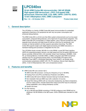
LPC540xxNXP Semiconductors32-bit ARM Cortex-M4 microcontroller5. Block diagramFigure 4 shows the LPC540xx block diagram. In this figure, orange shaded blocks supportgeneral purpose DMA and yellow shaded blocks include dedicated DMA control.LPC540xxProduct data sheetDownloaded from Arrow.com.All information provided in this document is subject to legal disclaimers.Rev. 1.9 — 23 October 2018 NXP Semiconductors N.V. 2018. All rights reserved.9 of 168
LPC540xxNXP Semiconductors32-bit ARM Cortex-M4 microcontrollerJTAG test andISP access boundary scaninterfaceportDEBUG INTERFACEARM CORTEX-M4WITH FPU/MPUI-codebusethernetPHY interfaceLCDpanelFS USBbusSDIOinterfaceETHERNET10/100MAC AVBLCDPANELINTERFACEUSB interfaceCANFDXtalin XtaloutCANFDSHAD-code systembusbusRSTclocksandcontrolsCLOCK GENERATION,POWER CONTROL,AND OTHERSYSTEM FUNCTIONSCLKOUTinternalpowerVOLTAGE REGULATORVddBOOT ROM64 kBHS USBPHYHS USBbusSRAM192 kBSPI FLASHINTERFACESPIFISRAM64 kBSRAM32 kBMULTILAYERAHB MATRIXSRAM32 kBSRAM32 kBSHA SLAVEINTERFACEFS USBHOSTREGISTERSHS USBHOSTREGISTERSPOLYFUSEOTP 256 b12b ADC12-CHTEMPSENSORUSB RAMINTERFACESRAM8 kBSTATIC/DYNAMIC EXTMEMORY CONTROLLERHS GISTERSFS USBDEVICEREGISTERSCAN 0REGISTERSCAN 1REGISTERSETHERNETREGISTERSHS USBDEVICEREGISTERSCRCENGINEAPB slave group 0SYSTEM CONTROLAHB TOAPB BRIDGESCTimer/PWMSDIOREGISTERSAUDIO SUBSYSD-MIC,DECIMATOR, ETCAHB TOAPB BRIDGEFlexComms 0-4-UARTs 0-4 - I2Cs 0-4-SPI0s 0-4FlexComms 5-9-UARTs 5-9-SPI0s 5-9-I2Cs 5-9 - I2Ss 0,1SYSTEM CONTROL (async regs)2 x 32-BIT TIMERS (T3, 4)APB slave group 1GPIO INTERRUPT CONTROLPMU REGS ( BB, PVT)PERIPH INPUT MUX SELECTS32-BIT TIMERS (T2)2 x 32-BIT TIMERS (T0, 1)RITMULTI-RATE TIMER2 x SMARTCARDSOTP CONTROLLERRANDOM NUMBER GENRTC ALARMWATCHDOGOSCD[31:0]A[25:0]controlGPIOAPB slave group 2ASYNC AHB TOAPB BRIDGEI/O CONFIGURATIONGPIO GLOBAL INTRPTS (0, 1)ADCinputsWINDOWED WDTREAL TIMECLOCKRTC POWERDOMAINDIVIDER32 kHzOscMICRO TICK TIMERNote:- Orange shaded blocks support Gen. Purpose DMA.- Yellow shaded blocks include dedicated DMA Ctrl.Fig 4.aaa-029063LPC540xx Block diagramLPC540xxProduct data sheetDownloaded from Arrow.com.All information provided in this document is subject to legal disclaimers.Rev. 1.9 — 23 October 2018 NXP Semiconductors N.V. 2018. All rights reserved.10 of 168
LPC540xxNXP Semiconductors32-bit ARM Cortex-M4 microcontroller6. Pinning information6.1 Pinningball A1index area1 2 3 4 5 6 7 8 9 10 11 12 13 14ABCDEFGHJKLMNPaaa-026026Transparent top viewFig 5.TFBGA 180 Pin configurationball A1index area123456789 10ABCDEFGHJKaaa-029079Transparent top viewFig 6.LPC540xxProduct data sheetDownloaded from Arrow.com.TFBGA 100 Pin configurationAll information provided in this document is subject to legal disclaimers.Rev. 1.9 — 23 October 2018 NXP Semiconductors N.V. 2018. All rights reserved.11 of 168
LPC540xxNXP Semiconductors15720832-bit ARM Cortex-M4 microcontroller15652105531041aaa-026027Fig 7.LQFP 208 Pin configuration752551LPC540xxProduct data sheetDownloaded from Arrow.com.5026Fig 8.761001aaa-029081LQFP 100 Pin configurationAll information provided in this document is subject to legal disclaimers.Rev. 1.9 — 23 October 2018 NXP Semiconductors N.V. 2018. All rights reserved.12 of 168
LPC540xxNXP Semiconductors32-bit ARM Cortex-M4 microcontroller6.2 Pin descriptionOn the LPC540xx, digital pins are grouped into several ports. Each digital pin can supportseveral different digital functions (including General Purpose I/O (GPIO)) and anadditional analog function.100-pin, LQFPC4D619693[2]DescriptionType208-pin, LQFPPIO0 0Reset state[1] [9]Symbol180-pin, TFBGAPin description100-pin, TFBGATable 4.PU; Z I/O PIO0 0 — General-purpose digital input/output pin.Remark: In ISP mode, this pin is set to the Flexcomm 3 SPISCK function.ICAN1 RD — Receiver input for CAN 1.I/O FC3 SCK — Flexcomm 3: USART or SPI clock.PIO0 1A1A1207100[2]OCTimer MAT0 — Match output 0 from Timer 0.ISCT0 GPI0 — Pin input 0 to SCTimer/PWM.OPDM0 CLK — Clock for PDM interface 0, for digitalmicrophone.PU;I/O PIO0 1 — General-purpose digital input/output pin.ZPU;Remark: In ISP mode, this pin is set to the Flexcomm 3 SPIZSSEL0 function.OCAN1 TD — Transmitter output for CAN 1.I/O FC3 CTS SDA SSEL0 — Flexcomm 3: USARTclear-to-send, I2C data I/O, SPI Slave Select 0.PIO0 2/TRSTA7E917483[2]ICT0 CAP0 — Capture input 0 to Timer 0.ISCT0 GPI1 — Pin input 1 to SCTimer/PWM.IPDM0 DATA — Data for PDM interface 0 (digitalmicrophone).PU; Z I/O PIO0 2 — General-purpose digital input/output pin. Inboundary scan mode: TRST (Test Reset).Remark: In ISP mode, this pin is set to the Flexcomm 3 SPIMISO function.I/O FC3 TXD SCL MISO — Flexcomm 3: USART transmitter,I2C clock, SPI master-in/slave-out data.ICT0 CAP1 — Capture input 1 to Timer 0.OSCT0 OUT0 — SCTimer/PWM output 0.ISCT0 GPI[2] — Pin input 2 to SCTimer/PWM.I/O EMC D[0] — External Memory interface data [0].LPC540xxProduct data sheetDownloaded from Arrow.com.All information provided in this document is subject to legal disclaimers.Rev. 1.9 — 23 October 2018 NXP Semiconductors N.V. 2018. All rights reserved.13 of 168
LPC540xxNXP Semiconductors32-bit ARM Cortex-M4 microcontroller85[2]DescriptionTypeA10 178Reset state[1] [9]A6100-pin, LQFPPIO0 3/TCK208-pin, LQFP180-pin, TFBGAPin description continuedSymbol100-pin, TFBGATable 4.PU; Z I/O PIO0 3 — General-purpose digital input/output pin. Inboundary scan mode: TCK (Test Clock In).Remark: In ISP mode, this pin is set to the Flexcomm 3 SPIMOSI function.I/O FC3 RXD SDA MOSI — Flexcomm 3: USART receiver,I2C data I/O, SPI master-out/slave-in data.OCT0 MAT1 — Match output 1 from Timer 0.OSCT0 OUT1 — SCTimer/PWM output 1.ISCT0 GPI3 — Pin input 3 to SCTimer/PWM.R — Reserved.I/O EMC D[1] — External Memory interface data [1].PIO0 4/TMSB6C818587[2]PU; Z I/O PIO0 4 — General-purpose digital input/output pin. Inboundary scan mode: TMS (Test Mode Select).Remark: The state of this pin at Reset in conjunction withPIO0 5 and PIO0 6 will determine the boot source for thepart or if ISP handler is invoked. See the Boot Processchapter in UM11060 for more details.ICAN0 RD — Receiver input for CAN 0.I/O FC4 SCK — Flexcomm 4: USART or SPI clock.ICT3 CAP0 — Capture input 0 to Timer 3.ISCT0 GPI4 — Pin input 4 to SCTimer/PWM.R — Reserved.I/O EMC D[2] — External Memory interface data [2].OPIO0 5/TDIA5E718989[2]ENET MDC — Ethernet management data clock.PU; Z I/O PIO0 5 — General-purpose digital input/output pin.In boundary scan mode: TDI (Test Data In).Remark: The state of this pin at Reset in conjunction withPIO0 4 and PIO0 6 will determine the boot source for thepart or if ISP handler is invoked. See the Boot Processchapter in UM11060 for more details.OCAN0 TD — Transmitter output for CAN 0.I/O FC4 RXD SDA MOSI — Flexcomm 4: USART receiver,I2C data I/O, SPI master-out/slave-in data.OCT3 MAT0 — Match output 0 from Timer 3.ISCT0 GPI5 — Pin input 5 to SCTimer/PWM.R — Reserved.I/O EMC D[3] — External Memory interface data [3].I/O ENET MDIO — Ethernet management data I/O.LPC540xxProduct data sheetDownloaded from Arrow.com.All information provided in this document is subject to legal disclaimers.Rev. 1.9 — 23 October 2018 NXP Semiconductors N.V. 2018. All rights reserved.14 of 168
LPC540xxNXP Semiconductors32-bit ARM Cortex-M4 microcontroller100-pin, LQFPA4A519190[2]DescriptionType208-pin, LQFPPIO0 6/TDOReset state[1] [9]180-pin, TFBGAPin description continuedSymbol100-pin, TFBGATable 4.PU; Z I/O PIO0 6 — General-purpose digital input/output pin. Inboundary scan mode: TDO (Test Data Out).Remark: The state of this pin at Reset in conjunction withPIO0 4 and PIO0 5 will determine the boot source for thepart or if ISP handler is invoked. See the Boot Processchapter in UM11060 for more details.I/O FC3 SCK — Flexcomm 3: USART or SPI clock.ICT3 CAP1 — Capture input 1 to Timer 3.OCT4 MAT0 — Match output 0 from Timer 4.ISCT0 GPI6 — Pin input 6 to SCTimer/PWM.R — Reserved.I/O EMC D[4] — External Memory interface data [4].IPIO0 7F9H12 12561[2]ENET RX DV — Ethernet receive data valid.PU; Z I/O PIO0 7 — General-purpose digital input/output pin.I/O FC3 RTS SCL SSEL1 — Flexcomm 3: USARTrequest-to-send, I2C clock, SPI slave select 1.OSD CLK — SD/MMC clock.I/O FC5 SCK — Flexcomm 5: USART or SPI clock.I/O FC1 SCK — Flexcomm 1: USART or SPI clock.OPDM1 CLK — Clock for PDM interface 1, for digitalmicrophone.I/O EMC D[5] — External Memory interface data [5].IPIO0 8E9H10 13364[2]ENET RX CLK — Ethernet Receive Clock (MII interface)or Ethernet Reference Clock (RMII interface).PU; Z I/O PIO0 8 — General-purpose digital input/output pin.I/O FC3 SSEL3 — Flexcomm 3: SPI slave select 3.I/O SD CMD — SD/MMC card command I/O.I/O FC5 RXD SDA MOSI — Flexcomm 5: USART receiver,I2C data I/O, SPI master-out/slave-in data.OSWO — Serial Wire Debug trace output.IPDM1 DATA — Data for PDM interface 1 (digitalmicrophone).I/O EMC D[6] — External Memory interface data [6].LPC540xxProduct data sheetDownloaded from Arrow.com.All information provided in this document is subject to legal disclaimers.Rev. 1.9 — 23 October 2018 NXP Semiconductors N.V. 2018. All rights reserved.15 of 168
LPC540xxNXP Semiconductors32-bit ARM Cortex-M4 microcontroller65[2]DescriptionType100-pin, LQFP208-pin, LQFPE10 G12 136180-pin, TFBGAPIO0 9Reset state[1] [9]Pin description continuedSymbol100-pin, TFBGATable 4.PU; Z I/O PIO0 9 — General-purpose digital input/output pin.I/O FC3 SSEL2 — Flexcomm 3: SPI slave select 2.OSD POW EN — SD/MMC card power enable.I/O FC5 TXD SCL MISO — Flexcomm 5: USART transmitter,I2C clock, SPI master-in/slave-out data.R — Reserved.I/O SCI1 IO — SmartCard Interface 1 data I/O.I/O EMC D[7] — External Memory interface data [7].PIO0 10/ADC0 0J1P25023[4]PU; Z I/O; PIO0 10/ADC0 0 — General-purpose digital input/outputAI pin. ADC input channel 0 if the DIGIMODE bit is set to 0 inthe IOCON register for this pin.I/O FC6 SCK — Flexcomm 6: USART, SPI, or I2S clock.ICT2 CAP2 — Capture input 2 to Timer 2.OCT2 MAT0 — Match output 0 from Timer 2.I/O FC1 TXD SCL MISO — Flexcomm 1: USART transmitter,I2C clock, SPI master-in/slave-out data.R — Reserved.OPIO0 11/ADC0 1K1L35124[4]SWO — Serial Wire Debug trace output.PU; Z I/O; PIO0 11/ADC0 1 — General-purpose digital input/outputAI pin. ADC input channel 1 if the DIGIMODE bit is set to 0 inthe IOCON register for this pin.I/O FC6 RXD SDA MOSI DATA — Flexcomm 6: USARTreceiver, I2C data I/O, SPI master-out/slave-in data, I2Sdata I/O.OCT2 MAT2 — Match output 2 from Timer 2.IFREQME GPIO CLK A — Frequency Measure pin clockinput A.R — Reserved.R — Reserved.ILPC540xxProduct data sheetDownloaded from Arrow.com.SWCLK — Serial Wire Debug clock. This is the defaultfunction after booting.All information provided in this document is subject to legal disclaimers.Rev. 1.9 — 23 October 2018 NXP Semiconductors N.V. 2018. All rights reserved.16 of 168
LPC540xxNXP Semiconductors32-bit ARM Cortex-M4 microcontroller100-pin, LQFPJ2M35225[4]DescriptionType208-pin, LQFPPIO0 12/ADC0 2Reset state[1] [9]180-pin, TFBGAPin description continuedSymbol100-pin, TFBGATable 4.PU; Z I/O; PIO0 12/ADC0 2 — General-purpose digital input/outputAI pin. ADC input channel 2 if the DIGIMODE bit is set to 0 inthe IOCON register for this pin.I/O FC3 TXD SCL MISO — Flexcomm 3: USART transmitter,I2C clock, SPI master-in/slave-out data.R — Reserved.IFREQME GPIO CLK B — Frequency Measure pin clockinput B.ISCT0 GPI7 — Pin input 7 to SCTimer/PWM.R — Reserved.I/O SWDIO — Serial Wire Debug I/O. This is the defaultfunction after booting.PIO0 13C10 F1114167[3]ZI/O PIO0 13 — General-purpose digital input/output pin.Remark: In ISP mode, this pin is set to the Flexcomm 1 I2CSDA function.I/O FC1 CTS SDA SSEL0 — Flexcomm 1: USARTclear-to-send, I2C data I/O, SPI Slave Select 0.IUTICK CAP0 — Micro-tick timer capture input 0.ICT0 CAP0 — Capture input 0 to Timer 0.ISCT0 GPI0 — Pin input 0 to SCTimer/PWM.R — Reserved.R — Reserved.IPIO0 14D9E13 14469[3]ZENET RXD0 — Ethernet receive data 0.I/O PIO0 14 — General-purpose digital input/output pin.Remark: In ISP mode, this pin is set to the Flexcomm 1 I2CSCL function.I/O FC1 RTS SCL SSEL1 — Flexcomm 1: USARTrequest-to-send, I2C clock, SPI slave select 1.IUTICK CAP1 — Micro-tick timer capture input 1.ICT0 CAP1 — Capture input 1 to Timer 0.ISCT0 GPI1 — Pin input 1 to SCTimer/PWM.R — Reserved.R — Reserved.ILPC540xxProduct data sheetDownloaded from Arrow.com.ENET RXD1 — Ethernet receive data 1.All information provided in this document is subject to legal disclaimers.Rev. 1.9 — 23 October 2018 NXP Semiconductors N.V. 2018. All rights reserved.17 of 168
LPC540xxNXP Semiconductors32-bit ARM Cortex-M4 microcontroller100-pin, LQFPK2L45326[4]DescriptionType208-pin, LQFPPIO0 15/ADC0 3Reset state[1] [9]180-pin, TFBGAPin description continuedSymbol100-pin, TFBGATable 4.PU; Z I/O; PIO0 15/ADC0 3 — General-purpose digital input/outputAI pin. ADC input channel 3 if the DIGIMODE bit is set to 0 inthe IOCON register for this pin.I/O FC6 CTS SDA SSEL0 — Flexcomm 6: USARTclear-to-send, I2C data I/O, SPI Slave Select 0.IUTICK CAP2 — Micro-tick timer capture input 2.ICT4 CAP0 — Capture input 4 to Timer 0.OSCT0 OUT2 — SCTimer/PWM output 2.R — Reserved.PIO0 16/ADC0 4H3M45427[4]OEMC WEN — External memory interface Write Enable(active low).OENET TX EN — Ethernet transmit enable (RMII/MIIinterface).PU; Z I/O; PIO0 16/ADC0 4 — General-purpose digital input/outputAI pin. ADC input channel 4 if the DIGIMODE bit is set to 0 inthe IOCON register for this pin.wsI/O FC4 TXD SCL MISO — Flexcomm 4: USART transmitter,I2C clock, SPI master-in/slave-out data.OCLKOUT — Output of the CLKOUT function.ICT1 CAP0 — Capture input 0 to Timer 1.R — Reserved.R — Reserved.PIO0 17B10 E14 14670[2]OEMC CSN[0] — External memory interface static chipselect 0 (active low).OENET TXD0 — Ethernet transmit data 0.PU; Z I/O PIO0 17 — General-purpose digital input/output pin.I/O FC4 SSEL2 — Flexcomm 4: SPI slave select 2.ISD CARD DET N — SD/MMC card detect (active low).ISCT0 GPI7 — Pin input 7 to SCTimer/PWM.OSCT0 OUT0 — SCTimer/PWM output 0.R — Reserved.LPC540xxProduct data sheetDownloaded from Arrow.com.OEMC OEN — External memory interface output enable(active low)OENET TXD1 — Ethernet transmit data 1.All information provided in this document is subject to legal disclaimers.Rev. 1.9 — 23 October 2018 NXP Semiconductors N.V. 2018. All rights reserved.18 of 168
LPC540xxNXP Semiconductors32-bit ARM Cortex-M4 microcontroller72[2]DescriptionTypeC14 150Reset state[1] [9]C9100-pin, LQFPPIO0 18208-pin, LQFP180-pin, TFBGAPin description continuedSymbol100-pin, TFBGATable 4.PU; Z I/O PIO0 18 — General-purpose digital input/output pin.I/O FC4 CTS SDA SSEL0 — Flexcomm 4: USARTclear-to-send, I2C data I/O, SPI Slave Select 0.PIO0 19C5C619391[2]ISD WR PRT — SD/MMC write protect.OCT1 MAT0 — Match output 0 from Timer 1.OSCT0 OUT1 — SCTimer/PWM output 1.OSCI1 SCLK — SmartCard Interface 1 clock.OEMC A[0] — External memory interface address 0.PU; Z I/O PIO0 19 — General-purpose digital input/output pin.I/O FC4 RTS SCL SSEL1 — Flexcomm 4: USARTrequest-to-send, I2C clock, SPI slave select 1.IUTICK CAP0 — Micro-tick timer capture input 0.OCT0 MAT2 — Match output 2 from Timer 0.OSCT0 OUT2 — SCTimer/PWM output 2.R — Reserved.OEMC A[1] — External memory interface address 1.I/O FC7 TXD SCL MISO WS — Flexcomm 7: USARTtransmitter, I2C clock, SPI master-in/slave-out data I/O, I2Sword-select/frame.PIO0 20C8D13 15374[2]PU; Z I/O PIO0 20 — General-purpose digital input/output pin.I/O FC3 CTS SDA SSEL0 — Flexcomm 3: USARTclear-to-send, I2C data I/O, SPI Slave Select 0.OCT1 MAT1 — Match output 1 from Timer 1.ICT3 CAP3 — Capture input 3 to Timer 3.ISCT0 GPI2 — Pin input 2 to SCTimer/PWM.I/O SCI0 IO — SmartCard Interface 0 data I/O.OEMC A[2] — External memory interface address 2.I/O FC7 RXD SDA MOSI DATA — Flexcomm 7: USARTreceiver, I2C data I/O, SPI master-out/slave-in data, I2Sdata I/O.PIO0 21B9C13 15877[2]PU; Z I/O PIO0 21 — General-purpose digital input/output pin.I/O FC3 RTS SCL SSEL1 — Flexcomm 3: USARTrequest-to-send, I2C clock, SPI slave select 1.IUTICK CAP3 — Micro-tick timer capture input 3.OCT3 MAT3 — Match output 3 from Timer 3.ISCT0 GPI3 — Pin input 3 to SCTimer/PWM.OSCI0 SCLK — SmartCard Interface 0 clock.OEMC A[3] — External memory interface address 3.I/O FC7 SCK — Flexcomm 7: USART, SPI, or I2S clock.LPC540xxProduct data sheetDow
Product data sheet Rev. 1.9 23 October 2018 6 of 168 NXP Semiconductors LPC540xx 32-bit ARM Cortex-M4 microcontroller 3.1 Ordering options Table 2. Ordering options Type number Package Name SRAM/kB FS USB HS USB Ethernet AVB Classic CAN CAN FD LCD EMC data bus width (bit) Flexcomm Interface GPIO SHA Arrow.com.