Transcription
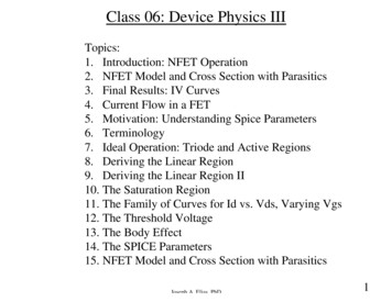
Class 06: Device Physics IIITopics:1. Introduction: NFET Operation2. NFET Model and Cross Section with Parasitics3. Final Results: IV Curves4. Current Flow in a FET5. Motivation: Understanding Spice Parameters6. Terminology7. Ideal Operation: Triode and Active Regions8. Deriving the Linear Region9. Deriving the Linear Region II10. The Saturation Region11. The Family of Curves for Id vs. Vds, Varying Vgs12. The Threshold Voltage13. The Body Effect14. The SPICE Parameters15. NFET Model and Cross Section with ParasiticsJoseph A. Elias, PhD1
Class 06: Device Physics IIINFET Model and Cross Section with Parasitics (Martin p.101) Goal is to understand the operation of an NFET shown in the model and cross section Last lectures covered the pn junctions of the source and drain, operation of the channel This lecture will cover the operation of the transistor as a whole Question - what type of component is gmVgs?Joseph A. Elias, PhD2
Class 06: Device Physics IIIFinal Results: IV Curves (Martin p.97) IV curves explain how the transistor performs when biased in different configurations SPICE model explains these IV curves in terms of physics-based parameters This lecture will concentrate on ideal behavior (triode/active); non-ideal(short channel) later How many terminals in a NFET? Answer: 4 (S-G-D-Sub) The IV curve above assumes source and substrate are shorted The IV curve above assumes Id really means current from drain to source Why is it called source and drain, and where is the current flowing to/from?Joseph A. Elias, PhD3
Class 06: Device Physics IIICurrent Flow in a FET (Martin p.87)sourcegrounddrainpositive potentialElectron flowCurrent flowsource is a “source of”drain is “draining”majority carriers flowCurrent flowNFETelectronselectronssource- drainIdrain- sourceJoseph A. Elias, PhDPFETholesholessource- drainIsource- drain4
Class 06: Device Physics IIIMotivation: Understanding Spice Parameters (Martin p.121) The ones not covered so far by lectures are: VTO, UO, LD, GAMMAJoseph A. Elias, PhD5
Class 06: Device Physics IIITerminology (Martin c.3)IDµnWLCoxVgsVtnVdsVds-satVeffDrain current, usually implying drain-to-source current (what else would it be?)Id -lin (linear) - current in the linear region (triode region)Id sat (saturation) - current in the saturation region (active region)Mobility of electronsWidth of channelLength of channelCapacitance of channel oxideGate to source potentialTransistor threshold for n-typeDrain to source potentialDrain to source potential in the saturation regimeVgs - Vtn, which gives the voltage amount above or below thresholdJoseph A. Elias, PhD6
Class 06: Device Physics IIIIdeal Operation: Triode and Active Regions (Martin p.94)Three regions of operation: Linear or Triode Region Saturation or Active Region Transition regionVds VeffVds VeffVdg Vt or Vds VeffJoseph A. Elias, PhDchannel invertedchannel pinched offbeginning of pinch off7
Class 06: Device Physics IIIDeriving the Linear Region (Martin c.3 Appendix)Similar to a resistorwhere the conductivity isand µn is the mobility of the carrier.n is density/volumeThis gives a current density ofThe total current flowing through a cube of dimensions W, L, H isThe voltage drop along the direction of current flow isCombining the above giveswhere n is a function of xIf one expresses n(x) as a function of charge density per unit squaregives the relationshipSince the voltage in the channel is not constant, one needs to relate the gate-source, threshold, andchannel potentials to the charge in the channel through Q CV. This formulates the vertical andhorizontal relationships.Joseph A. Elias, PhD8
Class 06: Device Physics IIIDeriving the Linear Region II (Martin c.3 Appendix)Substituting the charge density in thechannel into the current equationgivesIntegrating the equation from 0 dV Vds and from 0 dx L givesSolving for Id gives the linear region:For very small Vds (i.e., Vds Veff):Joseph A. Elias, PhD9
Class 06: Device Physics IIIThe Saturation Region (Martin p.93)What causes the current to saturate? As the drain voltage increases, the depletion region around the drain increases As the depletion region increases, the number of free carriers at the drain decreases The voltage at the drain is opposing the voltage from the gate, so the Vgd falls below Vtn This is referred to as pinch-off, since the channel carrier density is pinched One can then substitute Vds Vgs-Vtn into the linear equation to obtainJoseph A. Elias, PhD10
Class 06: Device Physics IIIThe Family of Curves for Id vs. Vds, Varying Vgs (Martin p.97)As one increases the gate to source bias, the location of the pinch off increasessince you now have more carriers in the channel.Short channel effects (to be discussed later):velocity saturationmobility degradationreduced output impedancehot-carrier effectsJoseph A. Elias, PhD11
Class 06: Device Physics IIIThe Threshold Voltage (Martin c.3 Appendix)(1)(2)(3)(4) The Vt implant is the “knob” used to control the behavior of the transistors Everything else in the equation is fixed for a given technologyJoseph A. Elias, PhD12
Class 06: Device Physics IIIThe Body Effect (Martin p.98, c.3 Appendix)As the bias on the substrate is made negative with respect to thesource (Vsb:Vsource-to-substrate is positive), the p-type carriers are pulledaway from the surface, increasing the depletion depth. This causes thechannel to become more difficult to invert, shifting the Vt to a morepositive value. The zero substrate bias is given as Vtn-0, and the bodyeffect modifies the Vtn as:This modifies the IV curve as:Joseph A. Elias, PhD13
Class 06: Device Physics IIIThe SPICE Parameters (Martin p.121)We have now discussed all of the above, except:Ld is related to the pinch-off region, how far the drain is located underneath the gateMJ, MJSW which are the non-abrupt junction parameters for a pn junctionJoseph A. Elias, PhD14
Class 06: Device Physics IIINFET Model and Cross Section with Parasitics (Martin p.101)Transconductance:Rds is the drain to source resistanceInfluence of body effect:Joseph A. Elias, PhD15
Class 06: Device Physics III Terminology (Martin c.3) I D Drain current, usually implying drain-to-source current (what else would it be?) Id -lin (linear) - current in the linear region (triode region) Id sat (saturation) - current in the saturation region (active region) µ n Mobility of electrons W Width of channel L Length of channel C


