Transcription
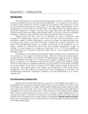
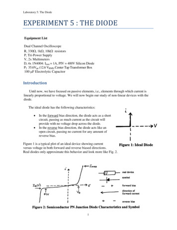
Laboratory 5: The DiodeEXPERIMENT 5 : THE DIODEEquipment ListDual Channel OscilloscopeR, 330 , 1k , 10k resistorsP, Tri-Power SupplyV, 2x MultimetersD, 4x 1N4004: Imax 1A, PIV 400V Silicon DiodeP2 35.6Vpp (12.6 VRMS) Center Tap Transformer Box100 F Electrolytic CapacitorIntroductionUntil now, we have focused on passive elements, i.e., elements through which current islinearly proportional to voltage. We will now begin our study of non-linear devices with thediode.The ideal diode has the following characteristics: In the forward bias direction, the diode acts as a shortcircuit, passing as much current as the circuit willprovide with no voltage drop across the diode.In the reverse bias direction, the diode acts like anopen circuit, passing no current for any amount ofreverse bias.Figure 1 is a typical plot of an ideal device showing currentversus voltage in both forward and reverse biased directions.Real diodes only approximate this behavior and look more like Fig. 2.1
Laboratory 5: The DiodeWe are interested in the solid state PN junction diode which has the following type ofcharacteristics. The diode’s symbol is an arrow with a bar, the arrow indicates the direction inwhich positive forward current flows. Figure 2 shows the positive forward bias needed to makethe diode conduct, VD, and the peak inverse voltage rating of the diode, PIV, beyond which thediode also conducts. Note that exceeding PIV is destructive (non-reversible breakdown) to manydiodes. The small reverse current, IR(T) is typically 10 pA for a silicon diode at roomtemperature and rapidly with increasing temperature, T. For example, at high temperatures (T 200 C) the junction no longer acts like a diode and passes in both directions. The diode’stemperatures will rise as current flows through the diode. Excessive temperature rise can becontrolled either by limiting the power the device dissipates for current in the forward directionor by employing a heat sink. The first approach implies a maximum current, Imax, for the diodein the forward direction.The real diode we will use is a silicon 1N4004 (400 V PIV, Imax 1 A) and the white line atone end indicates the direction in which positive forward current flows.Part I: Diode Characteristicsa) Set up the following circuit with V, on the 4 VDC scale. Use the protoboard to mount thediode. The resistor limits the current, regardless of what the diode does.b) Slowly increase the voltage from zero. Do not peg the meter. Record on the data sheetrepresentative values of voltage versus current. Do not exceed 100 mA.c) Power down.d) Draw a graph of I versus V and estimate VD.Figure 3: Diode Charactoristic Circuit.2
Laboratory 5: The DiodePart II: Half Wave RectifierPower generators usually produce AC voltages since they are most convenient for powertransmission. On the other hand, DC voltages are required for most electronic applications. Toproduce DC from AC (which usually has no DC component), it is necessary to redirect the ACcurrent flow in such a way as to produce a DC component, then to filter out the remaining ACcomponent. This is done by rectifying the signal to a single polarity, then filtering. The diode is arectifier and can be used to rectify AC voltages.a) Construct the following circuit. DC couple your oscilloscope.Figure 4: Center Tap Half Wave RectifierThe transformer converts 60 Hz 115 V RMS line voltage in the primary to 12.6 V RMS acrossthe secondary. The secondary has a center tap which can split the secondary into two 6.3 V RMSparts. The secondary is isolated from the primary. By grounding the bottom of the secondary (inthe figure), point 1 will be positive during a half cycle, then negative in the following half cycle.b) Use your scope to observe the voltage at point 1.c) Now observe the voltage across the resistor at point 2. Make sure that the scope is DCcoupled. (See what happens when the scope is AC coupled.) Draw the waveform at the 2output.d) This is an example of a half wave rectifier. Reverse the direction of the diode and draw thewaveform at the 2 output.Both configurations are called half-wave rectifiers; i.e., for one polarity the diode conductsand the input signal appears across the resistor, while for the opposite polarity the diode does notconduct and the input appears across the diode.This half-wave rectified signal can be filtered to produce a DC voltage but as a practicalmatter it seems we are wasting half of the generating capacity of the transformer by not utilizingthe other half of the generator signal.3
Laboratory 5: The DiodePart III: Full Wave Rectifiera) Construct the following circuit using the center tap of the secondary. DC coupleyour oscilloscope.b) Draw the resultant waveform across the resistor.This is an example of a full-wave rectifier. When the top loop is forward biased, the D, diodeconducts. When the bottom loop is forward biased, the D2 diode conducts. In either case, theforward current from the diode passes through the resistor in the same direction; thus, both halfcycles now have the same polarity. Note also that the rectified voltage across the resistor is thecenter tap peak voltage which is equal to one-half the peak secondary voltage.We can rectify the full secondary voltage with a bridge rectifier. Construct thefollowing circuit.c)4
Laboratory 5: The DiodeNote from the figure that opposite pairs of diodes steer the current through the resistor duringalternate half cycles, (D1, D3) then (D2, D4). Further, they steer the current in only one directionthrough the resistor depending on the polarity of the secondary. Finally, the rectified voltage is thefull voltage of the secondary.You might ask yourself why you don't use the second scope input to observe the secondary voltagewith this configuration. Can you guess what you would see? Take a look at the center tap with theB input. The problem is the position of the ground, which must be placed where it is to look acrossthe resistor.d) Leave this setup as is for the momentIV. The RC FilterNow that we have a rectified signal, we would like to convert it into a DC signal with as little ACripple as possible. A simple technique for low current cases is the capacitance filter. Consider theeffect of placing a 100 F capacitor across the load resistor, initially uncharged.On the very first half cycle as the secondary voltage rises from point 1 to 2 (solid line), diodes D2and D4 are forward biased and conduct, current flows through the resistor, and the capacitor ischarged up to VP. As the secondary voltage falls towards point 3, the capacitor cannot dischargeits positive charge through diode D2 or D, since they are reverse biased; thus, the voltage at point Adoes not follow the secondary. (A similar argument follows for the negative charge and diodesD, and D4.) However, the capacitor can discharge through𝑣(𝑡) 𝑣𝑝 𝑒 𝑡/𝜏(1)where the time constant in this case is 𝜏 𝑅𝐶 1𝑘Ω 100𝜇𝐹 100𝑚𝑠. At the same time, the11period of the full wave rectified signal is half that of line voltage, 𝑇 2𝑓 120𝐻𝑧 8.5 𝑚𝑠.Thus, the RC time constant is much longer than the period of the full wave rectified signal, i.e.𝑇 𝜏. Since 𝑡 𝑇, we can make the approximation that5
Laboratory 5: The Diode𝑡𝑣(𝑡) 𝑣𝑝 (1 𝜏) 𝑜𝑟𝑡𝑉𝑇 𝑣𝑝 (1 𝜏)(2)over a half cycle. The capacitor discharges linearly until the secondary voltage reverses itself andclimbs to point 4 at which point diodes D1 and D3 conduct and recharge the capacitor back up toVP at point 5. Then the whole process repeats itself (dotted line).The AC peak-to-peak ripple voltage is just𝑝𝑝𝑉𝑟𝑖𝑝𝑝𝑙𝑒 𝑉𝑝 𝑉𝑇 𝑉𝑝 𝑇(3)𝜏The effective DC voltage is roughly Vp less half the peak-to-peak AC ripple magnitude, i.e.,𝑝𝑉𝑟𝑖𝑝𝑝𝑙𝑒 𝑝𝑝𝑉𝑟𝑖𝑝𝑝𝑙𝑒2 𝑉𝑝 𝑇2𝜏(4)𝑇𝑉𝐷𝐶 𝑉𝑝 (1 2 𝜏) 𝑉𝑝𝑉The AC ripple voltage riding on VDC is roughly triangular and the RMS value for a triangular waveform is 𝑅 . The 3effectiveness of the filter is given by the ripple factor𝑟 a)𝑉𝑟𝑅𝑀𝑆𝑉𝐷𝐶 2𝑇 3 𝜏(5)Determine the ripple factor experimentally and theoretically for R 1k and 10k . When you connect the100 F capacitor to the full wave bridge, be sure to observe the proper polarity. To measure the AC ripple ridingon a large DC background, switch to AC coupling on your oscilloscope. With the DC component blockedyou can increase the gain of the oscilloscope to measure the peak-to-peak ripple voltage.6
Laboratory 5: The DiodeNAMESNote that the DC voltage and the ripple factor depend on the load. How they change with load isa measure of the regulation of the power supply. We will find latter that there are ways ofimproving the regulation of DC power supplies.7
you can increase the gain of the oscilloscope to measure the peak-to-peak ripple voltage. Laboratory 5: The Diode 7 NAMES_ Note that the DC voltage and the ripple factor depend on the load. How they change with load is a measure of the regulation of the