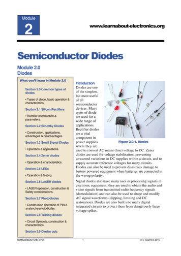
Transcription
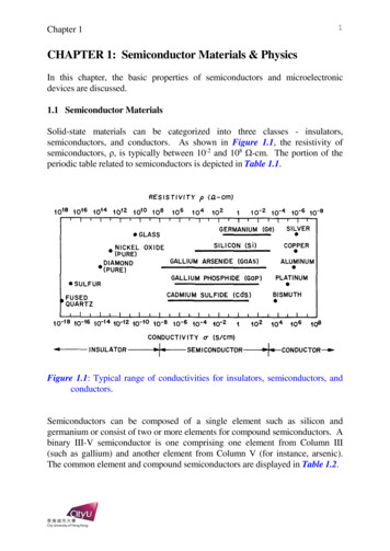
Chapter 11CHAPTER 1: Semiconductor Materials & PhysicsIn this chapter, the basic properties of semiconductors and microelectronicdevices are discussed.1.1 Semiconductor MaterialsSolid-state materials can be categorized into three classes - insulators,semiconductors, and conductors. As shown in Figure 1.1, the resistivity ofsemiconductors, ρ, is typically between 10-2 and 108 Ω-cm. The portion of theperiodic table related to semiconductors is depicted in Table 1.1.Figure 1.1: Typical range of conductivities for insulators, semiconductors, andconductors.Semiconductors can be composed of a single element such as silicon andgermanium or consist of two or more elements for compound semiconductors. Abinary III-V semiconductor is one comprising one element from Column III(such as gallium) and another element from Column V (for instance, arsenic).The common element and compound semiconductors are displayed in Table 1.2.
2Chapter 1Table 1.1: Portion of the Periodic Table Related to Semiconductors.PeriodColumn iPSiliconPhosphorusGeAsGermanium luriumTable 1.2: Element and compound ndsPbSPbTe
Chapter 131.2 Crystal StructureMost semiconductor materials are single crystals. Figure 1.2 exhibits threecubic-crystal unit cells - simple cubic, body-centered cubic, and face-centeredcubic. The element semiconductors, silicon and germanium, have a diamondlattice structure as shown in Figure 1.3. This configuration belongs to the cubiccrystal family and can be envisaged as two interpenetrating fcc sublattices withone sublattice staggered from the other by one quarter of the distance along adiagonal of the cube. All atoms are identical in a diamond lattice, and each atomin the diamond lattice is surrounded by four equidistant nearest neighbors that lieat the corners of a tetrahedron. Most of the III-V semiconductors (e.g. GaAs)have a zincblende lattice (shown in Figure 1.3b) that is identical to a diamondlattice except that one fcc sublattice has Column III atoms (Ga) and the other hasColumn V atoms (As).Figure 1.2: Three cubic-crystal unit cells – (a) Simple cubic (b) Body-centeredcubic (c) Face-centered cubic.
4Chapter 1Figure 1.3: (a) Diamond lattice. (b) Zincblende lattice.
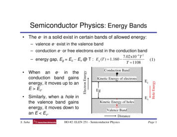
5Chapter 11.3 Energy BandsAccording to the Bohr model, the energy levels of a hydrogen atom are given byEquation 1.1: mo q 4 13.6EH 2 2 2 eV8 o h nn2(Equation 1.1)where mo denotes the free electron massq denotes the electronic chargeεo denotes the free space permittivityh denotes the Plank constantn denotes the principal quantum numberTherefore, for n 1, that is, ground state, EH -13.6 eV. For n 2, the firstexcited state, EH -3.4 eV.When two atoms approach one another, the energy level will split into two by theinteraction between the atoms. When N atoms come together to form a crystal,the energy will be split into N separate but closely spaced levels, therebyresulting in an essentially continuous band of energy. The detailed energy bandstructures of crystalline solids can be calculated using quantum mechanics.Figure 1.4 is a schematic diagram of the formation of a diamond lattice crystalfrom isolated silicon atoms. The energy band splits into two, the conductionband and the valence band, as the two atoms approach the equilibriuminteratomic spacing. The region separating the conduction and valence bands istermed the forbidden gap or bandgap, Eg. Figure 1.5 exhibits the energy banddiagrams of three classes of solids: insulators, semiconductors, and conductors.In insulators, the bandgap is relatively large and thermal energy or an appliedelectric field cannot raise the uppermost electron in the valence band to theconduction band. In metals or conductors, the conduction band is either partiallyfilled or overlaps the valence band such that there is no bandgap and current canreadily flow in these materials. In semiconductors, the bandgap is smaller thanthat of insulators, and thermal energy can excite electrons to the conduction band.The bandgap of a semiconductor decreases with higher temperature. Forinstance, for silicon, Eg is 1.12 eV at room temperature and 1.17 eV at zeroKelvin.
Chapter 16Figure 1.4: Formation of energy bands as a diamond lattice crystal by bringingtogether isolated silicon atoms.Figure 1.5: Schematic energy band representations of (a) an insulator, (b) asemiconductor, and (c) conductors.Figure 1.6 shows a more detailed schematic of the energy band structures forsilicon and gallium arsenide in which the energy is plotted against the crystalmomentum for two crystal directions. For silicon, the minimum of theconduction band and the maximum of the valence band have different crystalmomenta. Silicon is therefore an indirect bandgap semiconductor as a change in
Chapter 17crystal momentum is required for an electron transition between the valence andconduction bands. On the contrary, GaAs is a direct bandgap semiconductor andgeneration of photons is more efficient.Figure 1.6: Energy band structures of Si and GaAs. Circles (o) indicate holes inthe valence bands and dots ( ) indicate electrons in the conductor bands.
8Chapter 11.4 Intrinsic Carrier ConcentrationThe probability that an electronic state with energy E is occupied by an electronis given by the Fermi-Dirac distribution function:f(E) 11 e(Equation 1.2)( E E F ) / kTwhere EF is the Fermi level, the energy at which the probability of occupation byan electron is exactly one-half. At room temperature, the intrinsic Fermi levellies very close to the middle of the bandgap.The effective density of states in the conduction band NC is equal to2[2πmnkT/h2]3/2. Similarly, the effective density of states in the valence band NVis 2[2πmpkT/h2]3/2. At room temperature, NC for silicon is 2.8 x 10¹⁹ atoms/cm3.For an intrinsic semiconductor, the number of electrons per unit volume in theconduction band is equal to the number of holes per unit volume in the valenceband. That is, n p ni where ni is the intrinsic carrier density. Since n NCexp{-(EC-EF)/kT} and p NVexp{-(EF-EV)/kT}, where n is the electron densityand p is the hole density, np ni2 NCNVexp{(EV-EC)/kT} NCNVexp{-Eg/kT}.Therefore,ni ( N C N V ) 1/ 2 exp{ Eg2kT}(Equation 1.3)For a doped, or extrinsic, semiconductor, the increase of one type of carriersreduces the number of the other type. Thus, the product of the two types ofcarriers remains constant at a given temperature. For Si, ni 1.45 x 1010 cm-3 andfor GaAs, ni 1.79 x 106 cm-3. GaAs has a lower intrinsic carrier density onaccount of its larger bandgap.(For derivation of the equations described in this section, please peruse therecommended textbooks.)
9Chapter 11.5 Donors and AcceptorsFigure 1.7a shows schematically the doping of a silicon crystal with an arsenicatom. The arsenic atom forms covalent bonds with its four adjacent siliconatoms, and the fifth electron becomes a conduction electron, thereby giving riseto a positively charged arsenic atom. As a consequence, the silicon crystalbecomes n-type and arsenic is called a donor. Boron, on the other hand, has onlythree outer shell electrons and is an acceptor in silicon. Impurities such asarsenic and boron have energy levels very close to the conduction band andvalence band, respectively, as indicated in Figure 1.8. Shallow donors oracceptors such as these exist in ionized form at room temperature becausethermal energy is sufficient to ionize them. This condition is called completeionization, that is, n NA or ND. Since n NCexp{-(EC-EF)/kT}, ND NCexp{(EC-EF)/kT} andEC - EF kT ln[NC/ND](Equation 1.4)One of the implications of Equation 1.4 is that (EC-EF) becomes smaller withincreasing ND, or in other words, the Fermi level moves closer to the bottom ofthe conduction band. Similarly, for p-type semiconductors, the Fermi levelmoves towards the top of the valence band with increasing acceptorconcentration.When both donors and acceptors are present simultaneously, the impurity presentat a higher concentration determines the type of conductivity in thesemiconductor. The electron in an n-type semiconductor is called the majoritycarrier, whereas the hole in n-type semiconductor is termed the minority carrier.Conversely, in a p-type semiconductor, holes are majority carriers and electronsare minority carriers.
Chapter 110Figure 1.7: Schematic bond pictures of (a) n-type Si with donor (arsenic) and (b)p-type Si with acceptor (boron).
Chapter 111Figure 1.8: Measured ionization energies for various impurities in Si and GaAs.The levels below the gap center are measured from the top of the valenceband and are acceptor levels unless indicated by D for donor level. Thelevels above the gap center are measured from the bottom of the conductorband and are donor levels unless indicated by A for acceptor level.
12Chapter 1Example 1.1A silicon wafer is doped with 1016 arsenic atoms/cm3. Find the carrierconcentrations and the Fermi level at room temperature (300K).SolutionAt 300K, we can assume complete ionization of impurity atoms. We have:n ND 1016 cm-3Thus,p ni2(1.45 x10¹⁰ ) 2 2.1x10 4 cm 316ND10The Fermi level measured from the bottom of the conduction band is given byEquation 1.8: NC 2.8 x10¹⁹ EC E F kT ln 0.0259 ln 0.206eV16 10 ND The Fermi level measured from the intrinsic Fermi level is: n N 1016 E F Ei kT ln kT ln D 0.0259 ln 0.354eV10 1.45 x10 ni ni Graphically, the band structure is:
13Chapter 11.6 Electron MobilityUsing the theorem of equipartition of energy, mnvth2/2 3kT/2, where mn is theelectron effective mass and vth is the average thermal velocity. Electrons in thesemiconductor therefore move rapidly in all directions. The thermal motion of anindividual electron can be visualized as a succession of random scattering fromcollisions with lattice atoms, impurity atoms, and other scattering centers. Theaverage distance between collisions is called the mean free path, and the averagetime between collisions is termed the mean free time, τc. When a small electricfield, ε, is applied to the semiconductor, each electron will experience a forceequal to -qε and will be accelerated in opposite direction to the electric field witha drift velocity, vn. By Newtonian physics, the momentum of the electron is forcetimes time, that is, equal to -qετc. Therefore, mnvn -qετc, orvn -[qτc/mn]ε(Equation 1.5)Equation 1.5 states that the drift velocity is proportional to the applied electricfield. The proportionality factor is called the electron mobility, µn, in units ofcm2/V-s. Hence,vn -µnε where µn qτc/mn(Equation 1.6)A similar expression can be written for holes:vp µpε(Equation 1.7)The negative sign is removed from Equation 1.7 because holes drift in the samedirection as the electric field.Carrier mobility depends on lattice scattering and impurity scattering. Latticescattering results from thermal vibrations of the lattice atoms. As latticevibration is more significant with increasing temperature, mobility decreases. Infact, at high temperature, lattice vibration dominates. Impurity scattering resultswhen a charge carrier travels past an ionized donor or acceptor. The probabilityof impurity scattering depends on the total impurity concentration. Unlike latticescattering, impurity scattering becomes less significant at high temperaturesbecause the carriers move faster and are less effectively scattered. Figure 1.9illustrates these effects.
Chapter 114Figure 1.9: Electron mobility in silicon versus temperature for various donorconcentrations. Insert shows the theoretical temperature dependence ofelectron mobility.
15Chapter 11.7 Resistivity and ConductivityConsider a semiconductor sample shown in Figure 1.10, which has a crosssectional area A, a length L, and a carrier concentration of n electrons/cm3.Suppose an electric field, ε, is applied to the sample. The electron currentdensity, Jn, flowing in the sample can be calculated by summing the product ofthe charge on each electron times the electron's velocity over all electrons perunit volume n. That is,nJn In/A ( qv ) -qnvn qnµnεi 1i(Equation 1.8)The total current, J, is equal to Jn (electrons) Jp (holes). Thus,J (qnµn qpµp)ε(Equation 1.9)This proportionality constant is known as the conductivity, σ. A more commonlyused term is the resistivity, ρ, which is the reciprocal of the conductivity. Thus,ρ σ-1 [q(nµn pµp)]-1(Equation 1.10)Generally, in extrinsic semiconductors, one of the two components is dominant.Therefore, for n-type semiconductors,ρ (qnµn)-1(Equation 1.11)For p-type semiconductors,ρ (qpµp)-1(Equation 1.12)Figure 1.11 depicts the measured resistivity for silicon and gallium arsenide at300K as a function of the impurity concentration.
Chapter 116Figure 1.10: Current conduction in a uniformly doped semiconductor bar withlength L and cross-sectional area A.Figure 1.11: Resistivity versus impurity concentration for Si and GaAs.
Chapter 117Example 1.2Using the mobility and diffusivity chart for Si at 300K as a function of impurityconcentration (top graph), find the room temperature resistivity of an n-typesilicon wafer doped with 1016 atoms/cm3 of phosphorus.SolutionAt room temperature, we assume that all donors are ionized. Thus,n N D 1016 cm 3We can also calculate the resistivity using Equation 1.11:11 0.48 cm 19qn n 1.6 x10 x1016 x1300The mobility n is obtained from the mobility chart.Alternatively, we can obtain the result graphically from Figure 1.11 also giving 0.48 -cm.
Chapter 1181.8 P-N JunctionWhen a p-type semiconductor is joined together with an n-type semiconductor byprocesses such as epitaxy, ion implantation, or diffusion, a p-n junction iscreated. Figure 1.12 illustrates the energy band structure for such a device. Thelarge carrier concentration gradients at a p-n junction cause carrier diffusion.Holes from the p-side diffuse into the n-side, and electrons from the n-sidediffuse into the p-side. This sets up an electric field, which in equilibrium,exactly counteracts these diffusion tendencies and thus permits no net transportof electrons or holes across the junction.When a small positive voltage is applied to the p-side, there will be a netmovement of holes flowing from the p-side to the n-side, thereby creating aforward bias situation. Conversely, if a negative voltage is applied to the p-side,i.e. reverse bias condition, the p-n junction becomes an open circuit. A p-njunction therefore acts as a diode.Figure 1.12: (a) Uniformly doped p-type and n-type semiconductors beforejunction formation. (b) Electric field in the depletion region and energyband diagram of a p-n junction in thermal equilibrium.
Chapter 1191.9 Generation and Recombination ProcessesWhen the thermal equilibrium in a semiconductor is perturbed, that is, theproduct, np, is no longer equal to ni2, by injection of excess carriers, processesexist to restore the system back to equilibrium (np ni2). If the released energyresults in the emission of a photon, the process is called radiative recombination(Figure 1.13), otherwise it is called nonradiative recombination. When excesscarriers are introduced to a direct-bandgap semiconductor such as GaAs, theprobability is high that electrons and holes will recombine directly and a photonis emitted.Light emitting diodes (LEDs) are p-n junctions that emit spontaneous radiation inultraviolet, visible, or infrared region under bias (Figure 1.14). The mostcommon visible LEDs are made of alloys of GaAs1-yPy, where y is the atomicfraction. The bandgap of the alloy depends on its composition, i.e. y, thusimplying that the emitted light frequency can be tailored by altering y. In theGaAs1-yPy alloy, if y is greater than 0.45, the material becomes indirect-bandgapsemiconductor and the probability for radiative transitions is quite small.However, special recombination centers can be incorporated to enhance theradiative probability, for instance, by doping the GaAs1-yPy crystal with nitrogencreating an electron trap level close to the bottom of the conduction band.Nitrogen forms an isoelectronic center as the chemical properties of phosphorusand nitrogen are quite similar.As shown in Figure 1.13c, when a photon of energy hυ12 impinges on an atomwhile it is in the excited state, the atom can be stimulated to make a transition tothe ground state and gives off another photon of energy hυ12 that is in phase withthe incident radiation. This process is called stimulated emission and forms thebasis of solid-state lasers. The radiation thus produced is monochromatic andcoherent.For indirect-bandgap semiconductors like silicon, a direct recombination processis unlikely because electrons at the bottom of the conduction band have nonzerocrystal momentum with respect to holes at the top of the valence band. A directtransition that conserves both energy and momentum is not possible without asimultaneous lattice interaction. Hence, the dominant recombination process isindirect transition, that is, via localized energy states in the forbidden bandgap.Impurities with energy levels in the bandgap can substantially enhance therecombination rate and reduce the lifetime of excess carriers.
Chapter 120Figure 1.13: The three basic transition processes between two energy levels.Black dots indicate the state of the atom. The initial state is at the left; thefinal state, after the transition process, is at the right. (a) Absorption. (b)Spontaneous emission. (c) Stimulated emission.
Chapter 1Figure 1.14: Semiconductors of interest as visible LEDs. Figure includesrelative response of the human eye.21
Chapter 1221.10 Metal-Oxide-Semiconductor Field-Effect Transistor (MOSFET)The most common element in an integrated circuit is the metal-oxidesemiconductor field-effect transistor (MOSFET). Fig. 1.15 shows the schematiccross section of two n-channel MOS transistors. In a MOSFET device, thechannel current is controlled by a voltage applied to a gate that is separated fromthe channel by an insulator typically made of SiO2. It works as a switch in thatwhen a positive voltage is applied to the gate, negative charges are attractedtowards the gate insulator. If the voltage is large enough, enough negativecharges accumulate underneath the gate dielectric to result in a conductive pathbetween the source and drain. In the enhancement mode, (Fig. 1.15a), thetransistor is normally off, and no current flows between the source and drain for agate voltage (VG) 0 V. A conducting channel is then induced by applying avoltage of the appropriate polarity (positive for n-channel MOSFET or negativefor p-channel MOSFET) to the gate. In the depletion-mode (Fig. 1.15b), aconducting channel already exists, and the device is on with no bias applied tothe gate. The channel is depleted of mobile carriers by applying a gate voltage.Figure 1.15: Schematic cross section of n-channel MOS transistors: (a)enhancement-type device and (b) depletion-type device.The complementary MOS (CMOS) schematically shown in Fig. 1.16 is ofparamount importance in the IC industry. It consists of a combination of nchannel and p-channel MOS transistors in series. If both transistors are of theenhancement type, only one of the two transistors, that is, either the p-channel orn-channel device, is turned on at any one time by a common gate voltage. Since
Chapter 123the two transistors are in series and one of them is turned off, very little current isdrawn in the steady state. This device is very useful in low-powermicroelectronics. A channel stop is shown in Figure 1.16. It prevents theformation of an inversion between the n- and p-channel devices underinterconnecting metallization.Figure 1.16: CMOS structure: (a) basic circuit and (b) cross-sections of pchannel and n-channel devices formed together.
24Chapter 11.11 Fabrication of Integrated CircuitsFigure 1.17 illustrates the sequence of forming a simple metal-oxidesemiconductor (MOS) capacitor. The fabrication process includes oxidation ofsilicon, patterning, etching, ion implantation, drive-in, and metallization, all ofwhich will be reviewed in subsequent sections. Even for a simple MOScapacitor, the overall process can be quite onerous. To demonstrate thecomplexity of IC fabrication, Figure 1.18 depicts a typical commercial process toproduce a complementary MOS or CMOS logic gate device. In spite of itscomplexity over simple NMOS or PMOS, the CMOS structure reduces theoverall power consumption and is used in many microprocessors and high-speed,low-voltage integrated circuits.Figure 1.17: Steps to form an MOS capacitor.
25Chapter 1Figure 1.18: The CMOS process.
Chapter 1 6 Figure 1.4: Formation of energy bands as a diamond lattice crystal by bringing together isolated silicon atoms. Figure 1.5: Schematic energy band representations of (a) an insulator, (b) a semiconductor, and (c) conductors. Figure 1.6 shows a more detailed schematic of the energy band structures for sili