Transcription
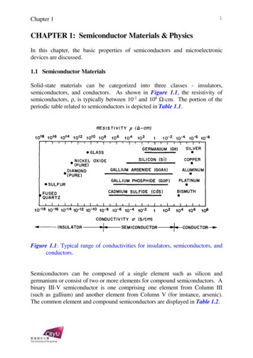
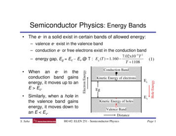
Semiconductor Physics: Energy Bands The e in a solid exist in certain bands of allowed energy:– valence e exist in the valence bandS. SahaKinetic Energy of electronsEcEgKinetic Energy of holesEv{Similarly, when a hole inthe valence band gainsenergy, it moves down toan E Ev.Conduction BandHole Energy When an e in theconduction band gainsenergy, it moves up to anE Ec.z Electron Energy– conduction e or free electrons exist in the conduction band7.02 x10 4 T 2– energy gap, Eg Ec Ev @ T : E g (T ) 1.160 (1)T 1108Valence BandDistanceHO #2: ELEN 251 - Semiconductor PhysicsPage 1
Intrinsic Semiconductors In a pure single crystalsemiconductor, all thee in the conductionbandare thermallyexcitedfromthevalence band. Then atany temperature, Tn p niwhere n free e- (cm-3)p free holes (cm-3)ni intrinsic carrier (cm-3). Note:– T ni – Eg ni S. SahaHO #2: ELEN 251 - Semiconductor PhysicsPage 2
Intrinsic Carrier ConcentrationThe product of the number of e and holes is given by:np ni2 (T ) CT 3e E g (T )kTE g (T )3 2 kT2(2)or, ni (T ) 3.9 x10¹⁶ T e ni 1.45x1010 cm-3 for silicon @ T 300oK.If T0 known reference temperature (generally, 300oK), thenat any temperature T, we can write:32 T ni (T ) ni (T0 ) e T0 E g (T ) E g (T0 ) 2 kT2 kT0(3)where, Eg(T) is given by (1). Eq. (3) is used in SPICE tocalculate ni at any temperature.S. SahaHO #2: ELEN 251 - Semiconductor PhysicsPage 3
Extrinsic Semiconductors To increase and control the conductivity of semiconductorswe add controlled amounts of “dopants” such as:– N type: P, As, and Sb each has five valence electrons– P type: B, Al, and Ga each has three valence electrons. These atoms occupy substitutional lattice sites and the extrae- or hole is very loosely bound, i.e. can easily move to theconduction or valence bands, respectively. In terms of banddiagrams this can be represented as:EcED1.1eV 0.05eVEvS. SahaDonorEc 0.05eV1.1eVEvEAAcceptorHO #2: ELEN 251 - Semiconductor PhysicsPage 4
Donor and Acceptor LevelsMeasured donor and acceptor levels for various impurities BAlGaIn1.12eVSiEv Acceptor levels are below the gap center and measured fromthe top of the valance band. Donor levels are above the gap center and measured from thebottom of the conduction band band.S. SahaHO #2: ELEN 251 - Semiconductor PhysicsPage 5
Density of StatesFermi LevelZero in forbidden bandEv EcThe probability that an allowed state is occupied is described bythe Fermi-Dirac distribution function:f(E) 1/[1 e(E EF)/kT](4)EF Fermi Level energy at which the probability of occupancy 1/2k Boltzmann constant; T temperature. Again, the probability of a state not being occupied is:(5)1 f(E) 1/[1 e(EF E)/kT] Probability a hole exists.S. SahaHO #2: ELEN 251 - Semiconductor PhysicsPage 6
Fermi Level: Temperature EffectAt T 0oK0.3T 0KT 100 KT 200 KT 300 KT 400 KT 500 KT 600 K0.2E - EF (eV)0.10.0all states EFare occupied. all states EFare empty.At T 0oK-0.1-0.2-0.30.0S. Saha 0.5f(E) some e haveE EF. someholesexist E EF.1.0HO #2: ELEN 251 - Semiconductor PhysicsPage 7
The Boltzmann ApproximationFor energies 3kT ( 75 meV @ room temp) above EF, f(E)can be approximated as:f(E) e (E EF)/kT]1.0f(E)F-D functionM-B function(6) Equation (5) representsMaxwell Boltzmannfunction. This approximation isquite good for manydevice applications, aswe will see later. However, for heavilydoped materials Fermifunction (4) must beused.0.5Approximation0.0-0.30.0E - EFS. Saha0.3HO #2: ELEN 251 - Semiconductor PhysicsPage 8
Summary of Equilibrium Carrier Distribution In an intrinsic or undoped semiconductor:n p ni 3.9x10¹⁶T3/2e Eg/2kT(2')EF (1/2)(Ec Ev) Ei(7)Fermi level EF in doped as well as undoped materials is given by:n nie(EF Ei)/kT nieq(φ φF)/kT(8)p nie(Ei EF)/kT nieq(φF φ)/kT(9)where φ Ei/q and φF EF/q. If both n- and p-type dopants are added in intrinsic semiconductor:n NA p ND(10)Then using np ni2, we can show for an n-type semiconductor:[ (1 / 2)[ N] N ] n / Nnn (1 / 2) N D2 4ni2 N D N DpnS. Saha2D 4ni2D2i(11)DHO #2: ELEN 251 - Semiconductor Physics(12)Page 9
Carrier Transport in Semiconductors In thermal equilibrium, mobile (conduction band) e- will be inrandom thermal motion.– avg. velocity of thermal motion, vth 107 cm/sec @ 300oK. In an applied ε field:– motion of e is in the directionopposite to ε.– this process is called drift andcauses a net current flow. Si CrystalεThe average e velocity called the drift velocity is given by:vd µε(13)where µ mobility qτ / m *τ mean free time between collision; m* effective mass of carrierS. SahaHO #2: ELEN 251 - Semiconductor PhysicsPage 10
Drift - ε Field Driven Motion vd µε linearrelationshipholds only forsmall fields. Mobility dependson parameterslike:– material– doping– temperature– scatteringmechanisms.S. SahaHO #2: ELEN 251 - Semiconductor PhysicsPage 11
Scattering Mechanisms Phonon scattering. Lattice atoms vibrate, and from QuantumMechanics we know that discrete allowed vibrational statesexist. This can be modeled as discrete particles calledphonons. Transfer of energy from electrons to the lattice iscalled phonon scattering. Ionized impurity atom scattering - important at high dopantconcentrations. Neutral impurity atom scattering - usually negligible. Carrier-carrier (e - e & e - hole) scattering - important athigh carrier concentrations. Surface scattering effects - important in MOSFET devices. Crystal defects - can be minimized by good crystals.S. SahaHO #2: ELEN 251 - Semiconductor PhysicsPage 12
µn Vs. TemperatureIonizedimpurityscattering is moreimportant at low T.Assuming that thedifferentscatteringmechanisms operateindependently:µ 1µLS. SahaHO #2: ELEN 251 - Semiconductor Physics 11µI .Page 13
Drift - ε Field Driven Motion At high fields, vd becomes comparable to vth which is anapproximate upper bound of vd. Thus, vd saturates and iscalled:vsat scattering limited velocity 1 x 107 cm/sec for e in Si 8 x 106 cm/sec for holes in Si.µoε The general expression for vd is: vd The critical field at which vsat occurs is: 2x10⁴ V/cm 2 V/µm. µoε β 1 vsat 1β(14)This is an important physical limit in very small semiconductordevices like MOSFETs.S. SahaHO #2: ELEN 251 - Semiconductor PhysicsPage 14
Drift - CurrentThe drift of carriers under an applied ε results in a current flow:I qAnvd(15)where A area; n number of e per unit volume.Substituting for vd µε and considering both e and holes:I/A (nqµn pqµp)ε(16)Usually, the majority carrier-term in (16) is important. Since fora semiconductor of length L under applied bias V, ε V/L, then:1/(qµnn qµpp) (V/L)/(I/A) (V/I)(A/L) R(A/L) ρwhere R ρ(L/A) resistance of the semiconductor:11 ρ (17)qµ n n qµ p p σwhere ρ resistivity in ohm.cm; σ conductivity in (ohm.cm)-1S. SahaHO #2: ELEN 251 - Semiconductor PhysicsPage 15
Resistivity Vs. Dopant Density @ T 300 KS. SahaHO #2: ELEN 251 - Semiconductor PhysicsPage 16
Diffusion - Gradient Driven MotionDiffusion occurs from high concentration regions towardslow concentration regions.Carrierconcentrationt1Flux ofdiffusioncurrentt2Flux ofdiffusioncurrentt1 t2 t3t30 xThe diffusion flux obeys Fick’s first law:F D(dn/dx)x(18)where F flux of carriersD diffusion constantn carrier density.S. SahaHO #2: ELEN 251 - Semiconductor PhysicsPage 17
Transport EquationsThe diffusion current through a cross-sectional area is:I qADn(dn/dx) qADp(dp/dx)(19)where Dn e diffusion constant 38 cm2/sec in SiDp hole diffusion constant 13 cm2/sec in SiDn and Dp are related to their respective carrier mobilities bythe Einstein relationship:Dp/µp Dn/µn kT/q(20)If both drift and diffusion are important,In qA[µnnε Dn(dn/dx)](21)Ip qA[µppε Dp(dp/dx)](22)We will use these basic equations in deriving devicecharacteristics.S. SahaHO #2: ELEN 251 - Semiconductor PhysicsPage 18
Generation-Recombination Thermal equilibrium is defined by the condition np ni2. Inthermal equilibrium, the equations discussed earlier may beused to calculate EF, n, p etc. However, the equilibrium condition may be disturbed by theintroduction or removal of free carriers.φ Injection: Extra carriers aregenerated by optical orelectrical means, and np ni2.NP S. Saha- Extraction: Here, carriersare removed electrically.And, as a result np ni2.HO #2: ELEN 251 - Semiconductor PhysicsPage 19
Injection of CarriersIf we shine light on the semiconductor with E hν Eg sothat e can be excited into the conduction band.n ni nLp ni pLINJECTIONn & p nizEchν EgEgEv{ν frequencyh Planck’s constantS. SahaHO #2: ELEN 251 - Semiconductor PhysicsPage 20
Low Level and High Level InjectionNow, if we shine light on an extrinsic semiconductor with:ND 1015 n this case:nnopnn ND nLp ni2/ND pLND 1015 cm-3Low level: nL NDHigh level: nL NDni for Si@ 300 oKpnoEquilibriumS. SahannnnpnLowlevelHighlevelIn Fig., a low level injection ofexcess carrier 1013 is shown.Since the mathematics for highlevel injection are complex, wewill consider only low levelinjection.HO #2: ELEN 251 - Semiconductor PhysicsPage 21
Direct (Band to Band) RecombinationIf we generate excess carriers ( n, p) at a rate GL due toincident light. Then for low level injection we can show that:z n electrons p n Uτ GLτEcWhere p p poEv{ p holes n n nop and n are total concentrations due to generationno and po are equilibrium concentrationsU net recombination rate GLτ excess carrier lifetime avg. time excess carriers remain free.Thus, τ p/GL p/U n/U(23)For band to band recombination, τn τp as the single phenomenaannihilates e and hole simultaneously.S. SahaHO #2: ELEN 251 - Semiconductor PhysicsPage 22
Direct Recombination Example:Net recombination rate U 1018 carriers cm-3 sec-1Minority-carrier lifetime τ 100 µsec,Then from (23), excess-carrier density: p n (1018) (100x10-6) 1014 cm-3. Summary:For a semiconductor with equilibrium carrier concentrations no andpo the steady state carrier concentrations under light are:S. Sahan no τGLnopo ni2p po τGLnp ni2HO #2: ELEN 251 - Semiconductor Physics(24)Page 23
Indirect Recombination (Trap-assisted)In Si and Ge this is often the dominant mechanism since theyare “indirect band gap semiconductors.” Physically this meansthat the minimum energy gap between Ec and Ev does notoccur at the same point in the momentum space.EEgEEcEvk“Direct band gapSemiconductor” GaAsEgEvEck“Indirect band gapSemiconductor” Si, GeSince momentum (k) must be conserved in any energy leveltransition, GaAs can easily make direct transitions which makesit useful for LEDs. Ep hν Eg. While Si and Ge tend torecombine through intermediate trapping levels.S. SahaHO #2: ELEN 251 - Semiconductor PhysicsPage 24
Indirect RecombinationEcEtEvLet us consider the following examplewhere an impurity like Au is introducedthat provides a “trapping level” or a setof allowed states at energy Et.The level Et is assumed to act like an acceptor, that is, it canbe neutral or negatively charged. Recombination isaccomplished by trapping an e- and a hole. (The analysiscan be easily extended to the case where the trap acts like adonor, i.e. and neutral charge states).Ec“1” e- capture12“2” e- emissionzzoEt“3” hole captureEiEF“4” hole emission431 3 or 3 1 recombinationEv{S. SahaHO #2: ELEN 251 - Semiconductor PhysicsPage 25
Indirect Recombination - SRH Shockley, Read, and Hall showed that for low level injection,the net recombination rate is given by:2vth σ N t ( pn ni )U (25) Et Ei n p 2 ni cosh kT wherevth carrier thermal velocity ( 107 cm/sec)σ carrier capture cross-section ( 10-15 cm2) From Eq (25) we observe:– the “driving force” or the rate of recombination is np ni2,(that is, the deviation from the equilibrium condition).– U 0 when np ni2.– U is maximum when Et Ei. That is, trapping levels near themid-band are the most efficient recombination centersS. SahaHO #2: ELEN 251 - Semiconductor PhysicsPage 26
Indirect Recombination - SRH Eq (25) shows that for Et Ec, U because: e capture is more probable while hole capture is less probable. e emission back to conduction band is highly probably. When Et Ei , from (25) we get:U vthσNt(pn - ni2)/[n p 2ni](26)a) N-type: n p and n ni, then from (26) τp 1/(vthpσpNt)(27)In N-type material, lots of e are around for capture. Therefore, thelimiting factor in recombination is the minority carrier lifetime τp.b) P-type: p n and p ni τn 1/(vthnσnNt)(28)Again, the limiting factor is the minority carrier lifetime.S. SahaHO #2: ELEN 251 - Semiconductor PhysicsPage 27
Quasi-Fermi LevelsUnder thermal equilibrium, we have:n nie(EF Ei)/kTp nie (EF Ei)/kTIn non-equilibrium conditions such as (1) injection (np ni2) or(2) extraction (np ni2), we cannot use these relationships.Here, we define two new quantities called quasi-Fermi levelssuch that the relationships of the type shown above hold and:n nie(EFn Ei)/kT(29)p nie (EFp Ei)/kT(30)where EFn e Quasi-Fermi level; EFp hole Quasi-Fermi level.EFn and EFp are the mathematical tools; their values are chosenso that the “correct” carrier concentrations are given in nonequilibrium situations.In general, EFn EFpS. SahaHO #2: ELEN 251 - Semiconductor PhysicsPage 28
Quasi-Fermi Levels: ExampleLet us consider a p-type semiconductor with NA 1016 cm-3, τ 10 µsec, and we shine light on it such that GL 1018 carrierscm-3 sec-1.Given, po NA 1016 cm-3τGL (10x10-6 sec)(1018 carriers cm-3 sec-1) 1013 carriers cm-3 n no τGL ni2/NA τGL 1013 cm-3p po τGL (1016 1013) 1016 cm-3Then from (29) and (30) we get:EFn Ei kTln(n/ni) 0.18 eV above EiEFp Ei kTln(p/ni) 0.36 eV below EiS. SahaEcn 1013 cm-3EFnEiEvEFpp 1016 cm-3HO #2: ELEN 251 - Semiconductor PhysicsPage 29
Quasi-Fermi LevelsIn example, since p po, EFp isessentially unchanged whileEFn moves up to reflect n noHere,E Fn E Fp2(31)pn n e kTiEcn 1013 cm-3EFnEiEvEFpp 1016 cm-3In equilibrium: EFn EFp EF pn ni2.However, under injection:EFn moves up towards the CB.EFp moves down towards the VB.Thus, EFn EFp is a measure of the degree of nonequilibrium in the semiconductor.We will use this concept of Quasi-Fermi levels in ourdiscussion of PN junctions.S. SahaHO #2: ELEN 251 - Semiconductor PhysicsPage 30
Non-Uniform Doping DistributionsIn our discussion of semiconductor statistics, we haveassumed spatially uniform doping levels. Often this is not thecase as we can see for the Bipolar Transistors.NBipolar TransistorN PxjBEN xjBCDepth1 The impurity profile we have drawn represents the fixedpositions of ionized donors and acceptors, i.e. ND , NA .2 The carriers (e and holes) are mobile and attempt to diffuseaway from regions of high concentrations.S. SahaHO #2: ELEN 251 - Semiconductor PhysicsPage 31
Non-Uniform Doping: Built-in Electric FieldNow, consider a simpler situation where we only have Ntype material (no junctions) but ND constant. Here,N1010141010 1 diffusion flux is given by: F Dn(dn/dx).18ND 2 as e move (drift) away, they leavebehind charged ions (ND ) whichxtry to pull e back.Equilibrium is established when diffusion drift. Here n(x) ND(x) and a “built-in” electric field that exists is given by:Ex (kT/q)(1/n)[dn/dx]Similarly for holes, Ex (kT/q)(1/p)[dp/dx](32)(33)This built-in Ε filed accelerates the minority carrier e injected into thebase from the emitter in their travel across the base or p-region.S. SahaHO #2: ELEN 251 - Semiconductor PhysicsPage 32
Basic Semiconductor Equations To this point we have discussed:– Carrier transport drift and diffusion– Carrier generation– Carrier recombination. The mechanism which ties all of these together is thecondition of continuity of current.Jp hole currentJp(x x)Jp(x)U recombination rateFrom the conservation of charge,U xS. Sahanet holesRate of change ofholesnumber of holes flowingrecombiningout of xin xHO #2: ELEN 251 - Semiconductor PhysicsPage 33
Continuity EquationsFrom our discussion of recombination,U holes recombining p poU x τpp poτp xNet holes flowing out of x11 Jp ( x x) Jp ( x)qq1 dJp xq dxS. SahaHO #2: ELEN 251 - Semiconductor PhysicsPage 34
Continuity EquationsFinally, the rate of change of holes within xdp xdt(decrease due to recombination)p po1 dJpdp x x xτpdtq dx dp1 dJp p po q dxτpdt(34)Similarly,dn1 dJn n no q dxτndt(35)Eq. (34) & (35), called the continuity equations, are fundamentallyimportant in the operation of semiconductor devices.S. SahaHO #2: ELEN 251 - Semiconductor PhysicsPage 35
Drift-Diffusion EquationsThe following equations that we previously derived are thetransport equations (21) and (22) and are alsofundamentally important in device operation.dnJp q( pµpε Dp )dxdnJn q(nµnε Dn )dxS. SahaHO #2: ELEN 251 - Semiconductor Physics(36)(37)Page 36
Poisson’s EquationOne final equation is needed to describe device operationand can be obtained from Poisson’s equation:ρdε dx KεoWhere ε electric fieldρ space charge density (charges/cm3)K dielectric constantεo permittivity of free space 8.854x10⁻¹⁴ F/cmTherefore,ρdxε KεoIf we know the charge density as f(x) we could find theelectric field.S. SahaHO #2: ELEN 251 - Semiconductor PhysicsPage 37
Poisson’s EquationIn general, the net charge density in a semiconductor isgiven by:ρ q[p ND n NA]dVFurthermore, ε dxqd 2V[(n p ) (NA ND )] so that2Kεodx(38)(34) (38) constitute a complete set of equations to describecarrier, current, and field distributions. Given appropriateboundary conditions, we can solve them for an arbitrary devicestructure. Generally, we will be able to simplify them based onphysical approximations.S. SahaHO #2: ELEN 251 - Semiconductor PhysicsPage 38
Intrinsic Carrier Concentration S. Saha HO #2: ELEN 251 - Semiconductor Physics Page 3 The product of the number of e and holes is given by: n i 1.45x1010 cm-3 for silicon @ T 300oK. If T 0 known reference temperature (generally, 300oK), then at any temperature T, we can write: where, E g(T) is given by (1).Eq. (3) is used in SPICE to calculate n i at any temperature.