Transcription
Lab ManualforEEL 4742CEmbedded SystemsDepartment of Electrical and Computer EngineeringRev. November 2018
ContentsPreface . . . . . . . . . . . . . . . . . . . . . . . . . . . . . . . . . . . . . . . . . . . .iiIntroduction . . . . . . . . . . . . . . . . . . . . . . . . . . . . . . . . . . . . . . . . . iiiReport Template . . . . . . . . . . . . . . . . . . . . . . . . . . . . . . . . . . . . . . .vi1 Flashing the LEDs . . . . . . . . . . . . . . . . . . . . . . . . . . . . . . . . . . . .12 Using the Push Buttons . . . . . . . . . . . . . . . . . . . . . . . . . . . . . . . . . 103 Using the Timer . . . . . . . . . . . . . . . . . . . . . . . . . . . . . . . . . . . . . 164 Interrupts & Low-Power Modes . . . . . . . . . . . . . . . . . . . . . . . . . . . . 245 LCD Display . . . . . . . . . . . . . . . . . . . . . . . . . . . . . . . . . . . . . . . 366 Advanced Timer Features . . . . . . . . . . . . . . . . . . . . . . . . . . . . . . . . 447 Concurrency via Interrupts . . . . . . . . . . . . . . . . . . . . . . . . . . . . . . . 548 Universal Asynchronous Receiver and Transmitter (UART) . . . . . . . . . . . . 589 Inter-Integrated Circuit (I2C) Communication . . . . . . . . . . . . . . . . . . . . 6810 Analog to Digital Converter (ADC) . . . . . . . . . . . . . . . . . . . . . . . . . . 7811 Serial Peripheral Interface (SPI) & LCD Pixel Display . . . . . . . . . . . . . . . . 86A I2C Functions . . . . . . . . . . . . . . . . . . . . . . . . . . . . . . . . . . . . . . 92i
PrefaceThis lab manual was developed at UCF for the course of EEL 4742C (Embedded Systems). Theteaching goal of this lab is to train the students in low-power microcontroller applications, todemonstrate the use of industry-class hardware and to write embedded software based on therecommended practices.If you have feedback about this manual or if you believe that you found a mistake, pleasesend your comments to Dr. Zakhia (Zak) Abichar at: zakhia17@ece.ucf.eduDr. AbicharNovember 2018UCFii
IntroductionIn this lab, we will learn designing embedded systems for low-power applications. Numerousembedded applications are low-power and run in the “bare metal” environment. This is an environment that doesn’t use an Operating System (OS) and where the software we write has fullcontrol over the hardware. The low-power embedded devices draw a very small current that cango down to micro-Amps and can operate on a small battery for years. Our choice of platform isthe Texas Instruments MSP430 architecture.We will use the microcontroller board and the sensor board that are listed below. The sensorboard has a variety of devices such as a light sensor, a temperature sensor, a 128x128 pixel LCDdisplay with 262K colors, a tri-color LED, a microphone, a buzzer and a 2D joystick. Microcontroller Board: Texas Instruments MSP430FR6989 LaunchPadPart number: MSP-EXP430FR6989 Sensor Board: Texas Instruments Educational BoosterPack Mark IIPart number: BOOSTXL-EDUMKIISkillsThe list below shows the skills that we will learn in this lab. Flashing the LEDs Using the push buttons Using the timer Programming interrupts Using the low-power modesiii
Using the segmented LCD display Using advanced timer features (multiple channels, timer-driven input/output) Providing concurrency via interrupts Performing communication with the UART, I2C and SPI protocols Using the Analog-to-Digital converter Programming pixel-based LCD graphicsLab Policy Lab attendance is required; up to two absences are allowed. All labs are weekly labs. The lab work should be demoed to the TA at the end of the session or by the start of thenext session. If an experiment is not finished in its session, the student should come to the lab after hoursto work on it and have it ready by the start of the next session. Lab access for after hours can be requested from the lab manager by following the instructions that are posted on the lab front door. Demoing the code to the lab instructor is required. The report will not be graded if thecode was not demoed. A lab report that contains the requested deliverables should be submitted for each experiment. The lab report is due by the start of the next session; seven days after the currentsession. Use the report template included in this manual. Having two or more reports not submitted may result in a failing grade in the class. The lab report is graded based on correctness, coding style and writing quality. In the summer session, the labs titled “LCD Display” and “Concurrency via Interrupts”are omitted.iv
Coding StyleIn this lab, we will practice writing code based on the recommended practices. The firstpractice is about modifying bits within a variable. Let’s say that we are interested in modifyingone bit of a variable. This implicitly means that all the other bits in this variable must remain unchanged. We should use AND, OR, XOR operations to clear, set or invert bits, respectively. Thesecond practice is avoiding the use of hexadecimal masks since they are hard to read, especiallywhen other people are reading our code. We should use symbolic masks instead.As an example, let’s set the rightmost bit of the variable Data. Out of the four cases below,the last one is the right way.Data 0x01; This statement is not correct since it changes all the other bits to zero.Secondly, hex masks should not be used.Data 0x01; This is technically correct since only the rightmost bit is modified.However, hex masks should be avoided.Data BIT0; This statement uses the symbolic mask (BIT0 00000001 0x01); however, it’s incorrect since it changes all the bits in the variable.Data BIT0; This statement is the right way. Only the rightmost bit changes and thecode is easily readable.Note that, in some cases, we purposefully want to modify all the bits in the variable suchas when we are configuring all the fields in a register. In this case, it is acceptable to use theassignment ‘ ’ operator (rather than using AND, OR, XOR). As an example, let’s say we wantto set the leftmost four bits of the variable Control and clear the rightmost four bits. Then, wecan write the statement below.Control BIT7 BIT6 BIT5 BIT4;These recommended practices should be used in all the experiments of this lab.v
Report TemplateEEL 4742C: Embedded SystemsName: .Lab number and titleIntroductionWrite a paragraph that introduces all your work in this lab experiment.Part 1: .Write a paragraph(s) that describes your approach to solving this part.Include your code.Answer the questions of this part.Part 2: .For each part, do the same as Part 1 aboveStudent Q&AAnswer the questions.ConclusionWrite a paragraph that has concluding notes on this lab experiment. Highlight what youlearned and the significant parts of this lab.vi
Lab 1Flashing the LEDsIn this lab, we will introduce the documentation files of the MSP430 boards and we will writesimple programs that flash the LEDs.1.1DocumentationAn essential part of programming microcontroller boards is using the documentation. ForMSP430 boards, each board has three documents. Below are the ones that corresponds to ourboard, the MSP430FR6989. MSP430FR6xx Family User’s Guide (slau367o) FR6xx Chip Data Sheet (slas789c) LaunchPad Board User’s Guide (slau627a)1
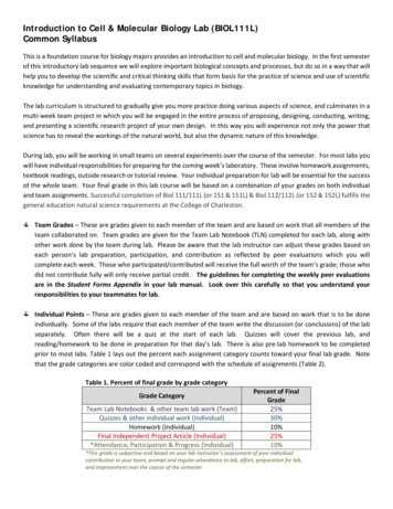
The terms in parentheses are the file identifiers. We can obtain these files from TI’s websiteor by searching for the file identifiers in a search engine. It’s a good idea to download these filesand keep them handy while doing the lab. Let’s look at the content of these files.The family user’s guide explains how the microcontroller’s components work. A microcontroller chip contains the CPU, memory and multiple peripherals such as timer, analog-to-digitalconverter, communication module, etc. The family user’s guide has a chapter for each of thesemodules. This file explains how the things work, hence, it’s a bit similar to a book. The contentof this file apply to a family of chips.The chip’s data sheet contains chip-specific information. It shows the pinout (what eachpin is used for), how a multi-use pin can be diverted to a specific function, the operating voltagelevels, the accuracy of internal clocks, etc. We mostly use the data sheet to lookup information.The LaunchPad board user’s guide is specific to a LaunchPad board and explains how theboard is wired and what external items are attached to the board. Typical attachments are LEDsand push buttons. This file shows to which pins the LEDs and buttons are attached and whetherthey are configured as active high or active low, which is needed to write the code. This file alsocontains the schematic of the LaunchPad board.The documentation for the Booster Pack is the following: Booster Pack User’s Guide (slau599a) Various data sheets for each component on the Booster PackThe first file shows the components that are connected to the Booster Pack such as the lightand temperature sensors, the buzzer, the display, etc. This file has general information on howthe components are connected together, but not on the inner working of these components. Foreach of the components, we would have to search for their specific data sheet from the respectivemanufacturer to see how they operate.1.2Flashing the LEDIn this part, we will run a code that flashes the red LED on the board. Start Code ComposerStudio (CCS) and click on the following menu items.File - New - CCS ProjectCreate a project and select the chip number as shown in Figure 1.1.2
Figure 1.1: Creating a project in Code Composer StudioOnce the project is created, copy and paste the code below in the main file1 . Let’s go throughthe main concepts in the code.The red LED is mapped to Port 1 Bit 0, in short P1.0. The header file (.h) included in thecode defines a bunch of masks that facilitate accessing bits. These masks are (BIT0 00000001),(BIT1 00000010), ., (BIT7 10000000). In general, BITn has all bits 0 except bit position n isequal to 1. Since the LED is mapped to P1.0, we’ll redefine BIT0 as redLED so we can accessthe LED using this mask.The variable ‘i’ is used in the delay loop. It counts from 0 to 20,000 to create a delay. Itis declared as volatile so the compiler doesn’t optimize away (eliminate) the delay loop. Thecompiler may assume the delay loop doesn’t do useful computation and eliminate it altogether.1Note that when the code is copied to the editor, the characters (inverse) and ˆ (xor) may get corrupted andneed to be retyped in the editor.3
If you suspect that the compiler is eliminating the delay loop, go to the menu item below andreduce the level of optimization to level 0.File - Properties - Build - MSP430 Compiler - OptimizationThe following line disables the WatchDog Timer (WDT) mechanism. This mechanismcauses periodic resets unless it’s periodically cleared explicitly by the code. It serves the purposeof protecting against software problems. We won’t use the WDT in this code, thus, we disableit.The following line clears the lock on the pins. Our board has nonvolatile memory. Uponstartup, the memory is locked to keep the old data it has. We clear the lock so we can write newdata to the memory and pins. Remember to include this line in every code you write, otherwise,the program most likely won’t perform any action.// Code that flashes the red LED#include msp430fr6989.h #define redLED BIT0// Red LED at P1.0void main(void) {volatile unsigned int i;WDTCTL WDTPW WDTHOLD;PM5CTL0 & LOCKLPM5;impedance modeP1DIR redLED;P1OUT & redLED;// Stop the Watchdog timer// Disable GPIO power-on default high-// Direct pin as output// Turn LED Offfor(;;) {// Delay loopfor(i 0; i 20000; i ) {}P1OUT ˆ redLED;// Toggle the LED}}The next two lines of code direct the pin as output and turn the LED off. Below, we can seethe variables that control a port. Port 1 is eight bits. Each bit can be used as input or output. The4
second variable P1DIR (direction), directs each pin as either output (1) or input (0). For all thepins that are directed as output, the variable P1OUT is used to write to them (0 or 1). For all thepins that are directed as input, the variable P1IN is used to read from them (0 or 1).Port 1:P1DIR:P1OUT:P1IN:1xSets a pin as input or outputWrite 0 or 1 to output pinsReads (0 or 1) from input pinsAccordingly, the red LED is mapped to bit 0, the rightmost bit. Then, we write 1 (output) toP1DIR at bit 0. To turn the LED on/off, we write to the variable P1OUT’s rightmost bit. Thesebits are marked above by 1 and x.When we change a bit to a specific value, it is necessary to leave the other bits in the variableunchanged. Hence, the code performs an OR operation on P1DIR, as shown below. The terms ato h designate the eight bits of P1DIR. We OR P1DIR with the mask redLED. Bit 0 becomes 1while all the other bits remain unchanged. This operation sets P1.0 to output so we can write tothe LED.P1DIR: abcd efghredLED: 0000 0001Result: abcd efg1P1OUT: abcd efgh redLED: 1111 1110Result: abcd efg0ORANDTo turn the LED off, we write 0 to its bit in P1OUT. This is an active high setting (1:on,0:off). We AND P1OUT with the inverse of redLED as shown above. Bit 0 becomes 0 while allthe other bits remain unchanged.In your codes throughout all the experiments of this lab, you should use masking operations(AND, OR, XOR) as above to change individual bits. It’s a bad practice to change all the bitswhen only one bit needs to be changed. Furthermore, hexadecimal masks should not be usedbecause the code wouldn’t be easily readable.The remaining of the code starts an infinite loop. Inside, a delay loop counts up to 20,000 andhas en empty body. When the delay elapses, the LED is toggled by applying the XOR operation.This is similar to the masking operations above. XORing a bit with 1 inverts it, while XORingthe remaining bits with 0 leaves them unchanged. Therefore, this operation toggles the LEDbetween on and off.5
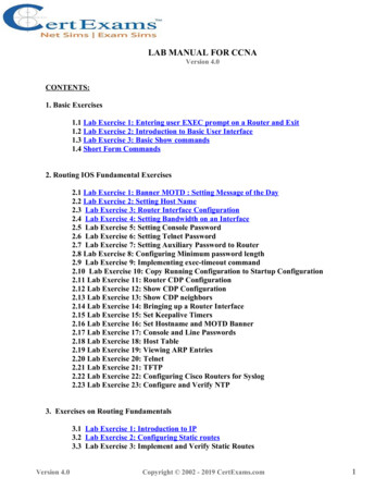
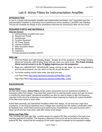
Running the CodeLet’s build (compile) this program, flash it to the board and run it. Click on the green bugbutton shown in Figure 1.2 to start the build process. The code is compiled and flashed tothe microcontroller. This is done via the JTAG (Joint Task Action Group) interface. JTAG ishardware on the board that allows programming the chip and enables debugging via CCS.Figure 1.2: Building (compiling) and launching a program.Once the code is built successfully, the green play button and red stop button, shown in thefigure, will appear. Click the green play button to start running the code in debug mode. In thedebug mode, the code is running on the chip under the supervision of Code Composer Studioand the JTAG for the purpose of debugging. For example, we can click the pause button andinspect all the variables and the registers in the program, as shown in Figure 1.3. We can evenchange the value of variables and registers before resuming the execution.Figure 1.3: Checking the variables and registers values in debug mode.It’s also possible to create a breakpoint at a line of code by double clicking next to the line ofcode before building the program. In debug mode, the execution stops automatically when thebreak point is reached.What happens if we click on the red stop button? We exit the debug mode and the codecontinues to run on the microcontroller in normal mode. While the debug mode and the normal6
mode generally exhibit the same behavior by the program, sometimes there is a difference in theprogram’s behavior. For example, the reset button works in normal mode but not in the debugmode.What happens if we unplug the board from the computer and plug it back? The code resumesrunning. It’s running completely off the board and the code is not lost when the power is gonesince it’s stored in a non-volatile memory.Perform the following actions: Change the upperbound value of ‘i’ to make the LED flash slower or fasterRun in debug mode; pause the code and check the variables and registers valuesRun in debug mode and test the reset button (the third button on the board); does it work?Run in normal mode and test the reset button; does it work?Disconnect the board from the computer and plug it back; does the code resume running?Deliverables: Demo your code to the lab instructor. In your report, submit a snapshot of the registers and variables values obtained from thedebug mode.1.3Setting a Long PeriodIn the previous code, the counter ‘i’ went from 0 to 20,000 to create a delay. To set a largerdelay, we can incrase the value of ‘i’. MSP430 is a 16-bit architecture. The registers and theALU are 16-bit. An integer (type int) created in our C program is treated as a 16-bit variable bythe compiler. An unsigned 16-bit variable can go from 0 up to 216 1, which is the range [0 65,535]. Accordingly, we can’t raise ‘i’ to higher than 64K.One interesting detail here is, on a desktop, an ‘int’ type is usually 32-bit, so how come it’s16-bit on the MSP430? The C standard specifies that an ‘int’ should be 16-bit or more. Hence,desktop platforms upgrade it to 32-bit while the MSP430 environment keeps it as 16-bit.Change the value of ‘i’ to 80,000 and run the code. Most likely the program will misbehavesince the 16-bit variable can’t go up to this value.Modify the code by writing nested delay loops or back-to-back delay loops to obtain a largedelay. This is a viable solution to obtain a large delay.Even though MSP430 is a 16-bit architecture, it’s possible to define 32-bit variables. Thecompiler maps such variables to two registers and perform all the manipulation to synthesize7
32-bit operations on the 16-bit CPU. To use this feature, use the include line shown below.Declare the variable of the type shown below. This corresponds to 32-bit unsigned integer. Thisis standard C syntax.#include stdint.h .volatile uint32 t i;// unsigned int 32-bit typeNow, test the code by setting the upperbound of the delay loop to 120,000. This should work.Deliverables: Demo your codes to the lab instructor. Submit your code with nested delay loop or back-to-back delay loop; show how you canobtain a large delay Submit your code using uint32 t data type; show how you can obtain a large delay1.4Flashing two LEDsIn this part, we will modify the code so that it flashes both LEDs that are connected to theboard. One is red the other is green. To which port/bit is the green LED mapped?One way to find out is to look at the board itself; it’s written in small font next to theLED. Another way to find this out is by looking at the LaunchPad user’s guide. Open this file(slau267a) on page 31. Find out where LED2 is connected. From the schematic, determineif this LED is active high (1:on, 0:off) or active low (0:on, 1:off).Modify the code so that it flashes both LEDs out of sync; when the green is on, the red is offand vice versa.Perform the following actions: Start by defining a mask for the green LED: #define greenLED BITx Set the green LED pin to output by applying an OR operation at PxDIR Initialize the green LED to on (so that it’s opposite of the red) by using an OR operationon PxOUT Toggle both LEDs inside the infinite loop by using XOR operationsIn the above, it’s up to you to determine the value of x in BITx, PxDIR, PxOUT.Deliverables:8
Demo your code to the lab instructor Include a screenshot of the board user’s guide schematic (p.31) that shows the LED connections Submit your code that flashes both LEDs out of sync This code can be easily modified to flash the LEDs in sync; insert one line in the code(comment it out) that shows how this can be done1.5Flashing Two LEDs at Different RatesWrite a code that flashes the red LED at twice the frequency of the green LED.Deliverables: Demo your code to the lab instructor Submit your codeStudent Q & ASubmit the answers to the questions in your report.1. In this lab, we used a delay loop to create a small delay; what is its effect on the batterylife if the device is battery operated? Is it a good way of generating delays?2. The MSP430 CPU runs on a clock that can be slowed down or sped up; what happensto the delay generated by the delay loop if the clock driving the CPU speeds up or slowsdown?3. How does the code run in the debug mode? Is the microcontroller running as an independent computer?4. How does the code run in the normal mode? Is the microcontroller running as an independent computer?5. In which mode does the reset button work?6. What is the data type uint16 t ? What about int16 t ? Are these standard C syntax?9
Lab 2Using the Push ButtonsIn this lab, we will learn using the push buttons of the LaunchPad board via a simple technique called polling.2.1Reading the Push ButtonsThe LaunchPad board is equipped with three push buttons, listed below:S1: Button connected to Port 1.1S2: Button connected to Port 1.2S3: Button connected to the reset (RST) pinThe buttons S1 and S2 are used for general-purpose and we’ll use them in this lab. The buttonS3 is connected to the reset pin and causes a reset when pushed. The reset pin can be re-purposed10
as an interrupt pin and, therefore, can be used as a general-purpose pin to some extent.The buttons S1 and S2 are connected in the active low configuration. That is, when they’repushed, they read as zero. Confirm this by looking at the schematic in the LaunchPad User’sGuide (slau627a) on page 31 and include a snapshot of the button schematics in your report.Port ConfigurationThe I/O ports are configured using the port configuration registers. These are presented inthe FR6xx Family User’s Guide (slau367o) in the chapter “Digital I/O” on page 363. Wesummarize the information that relates to this lab below in Table 2.1Table 2.1: Configuration Registers for Port 1P1DIRP1INP1RENPin direction(0: input) (1: output)Reading input pin(0: input is low) (1: input is high)Built-in resistor enable(can be set as pull-up or pull-down)(0: disable resistor) (1: enable resistor)P1OUTWrite to output (when direction is output)(0: write low) (1: write high)Configure resistor (when direction is input)(0: pull-down) (1: pull-up)A port (e.g: Port 1) is 8-bit and, accordingly, each of the variables shown in the table is 8-bit,with a one-to-one correspondence to the pins. We have already used P1DIR, P1IN and P1OUTin the previous lab.The configuration variable P1REN allows enabling a built-in resistor (inside the chip) foreach I/O pin. The built-in resistor is optionally used only when the I/O pin is configured asinput. We use P1REN to enable/disable the internal resistor. Furthermore, the resistor can beconfigured as pull-up (to Vcc) or pull-down (to ground). This is done via P1OUT. Note thatwhen the I/O pin is configured as input, P1OUT is not used for data. Therefore, it’s used toconfigure the resistor as pull-up or pull-down.In this lab, the I/O pins where the buttons are connected will be configured as input, thebuilt-in resistors will be enabled, and they will be set to pull-up. We can justify this by lookingat the buttons’ schematics. They’re connected to ground when they’re pushed. Therefore, we’llhave them pulled-up to Vcc so they read high when they’re released.11
Masking OperationTo read the button’s status, we need to inspect the button’s corresponding bit inside P1IN.Below are the two masking AND operations that allow reading a bit inside a variable. In thisexample, we’re reading BIT3 in the data.Data: ---- 0--BIT3: 0000 1000Result: 0000 0000Data: ---- 1--BIT3: 0000 1000Result: 0000 1000ANDANDOn the left side, the bit is 0 and the result of the AND operation is zero. On the right side,the bit is 1 and the result of the AND operations is nonzero. Please note that the result is notequal to 1, since the bit 1 is not on the rightmost position. For the case on the right side, wecan check if the result is nonzero, or if the result is equal to BIT3 Accordingly, the piece of codebelow shows how we check the bit’s value.// Check if bit is zeroif( (Data & BIT3) 0 ) .// Check if bit is one (two ways)if( (Data & BIT3) ! 0 ) .if( (Data & BIT3) BIT3 ) .Turning on the LED with the ButtonLet’s write a code that turns on the red LED when button S1 is pushed. As long as the buttonis held down, the red LED should remain on. When the button is released, the red LED shouldturn off. Below is the code, fill the missing parts. Please remember that using hexadecimalmasks is not allowed throughout all the experiments of this lab (we’ll use the masks BIT0, etc orredefined names e.g. redLED).// Turning on the red LED while button S1 is pushed#include msp430fr6989.h #define redLED BIT0#define greenLED BIT7#define BUT1 BIT1// Red LED at P1.0// Green LED at P9.7// Button S1 at P1.112
void main(void) {WDTCTL WDTPW WDTHOLD;PM5CTL0 & LOCKLPM5;// Stop the Watchdog timer// Enable the GPIO pins// Configure and initialize LEDsP1DIR redLED;// Direct pin as outputP9DIR greenLED;// Direct pin as outputP1OUT & redLED;// Turn LED OffP9OUT & greenLED;// Turn LED Off// Configure buttonsP1DIR & BUT1;P1REN .P1OUT .// Direct pin as input// Enable built-in resistor// Set resistor as pull-up// Polling the button in an infinite loopfor(;;) {// Fill the if-statement below.if ( . button S1 is pushed . )P1OUT redLED;// Turn red LED onelse P1OUT & redLED;// Turn red LED off}}This code polls the button infinitely and, therefore, keeps the CPU locked to this operation.A downside is the CPU can’t do another task. Secondly, if the device is battery-operated, pollingthe button infinitely could drain the battery. A more advanced approach is to setup the button viainterrupt and to put the microcontroller in low-power mode while waiting for the button push.We’ll explore this approach in a later lab.For this part, perform the following and include the answers in your report. Include snapshot of the buttons schematic from the LaunchPad User’s Guide. Explain whythe buttons are active low and why the pull-up resistor is used. Write the missing parts of the code and demo it to the TA. Submit the code in your report.13
2.2Using Two Push ButtonsModify the code from the previous part to control two LEDs using the two push buttons.When button S1 is pushed, the red LED should turn on. When button S2 is pushed, the greenLED should turn on. If both buttons are pushed simultaneously, both LEDs should turn on.For this part, perform the following: Write the code and demo it to the TA. Test the case when both buttons are pushed. Submit the code in your report.2.3Using Two Buttons with Exclusive AccessModify the code from the previous part so that the red LED is on while S1 is pushed and thegreen LED is on while S2 is pushed. However, the two LEDs should not be lit simultaneously.Imagine that they correspond to physical phenomena and a hazard occurs if both LEDs are lit atthe same time. Your software should ensure this doesn’t happen.Accordingly, the button that is pushed first has precedence. Let’s say S1 is held down andthe red LED is on. If, in the meanwhile, S2 is pushed, the green LED remains off and the redLED continues to be on. This state persists until S1 is released. Now, S2 has the chance to turnon the green LED. And, likewise, if S2 is held down with the green LED on, S1 is ignored whenpushed, until S2 is released.For this part, perform the following: Write the code and demo it to the TA. Stress test the code; what happens if both buttons are pushed simultaneously? Submit the code in your report.2.4Your Own DesignIn this part, combine elements from the previous parts and design an experiment that demonstrate the skills that you learned.Perform the following: Demo your code to the TA. In your report, describe the experiment and submit your code.14
Student Q&ASubmit the answers to the questions in your report.1. When a pin is configured as input, P1IN is used for data, which leaves P1OUT availablefor other use? In such case, what is P1OUT used for?2. A programmer wrote this line of code to check if bit 3 is equal to 1: if((Data &BIT3) 1). Explain why this if-statement is incorrect.3. Comment on the codes’ power-efficiency if the device is battery operated. Is reading thebutton via polling power efficient?15
Lab 3Using the TimerIn this lab, we will program the microcontroller’s timer module (Timer A) to generate timingevents. We will program two modes known as the continuous mode and the up mode. For bothmodes, we will use the polling technique, which is a simple approach based on reading a flagcontinuously.3.1The Continuous ModeThe MSP430FR6989 chip contains a timer module known as Timer A. This module is versatile and has many features. In this lab, we will use the module to time durations.The timer uses a clock signal of a known frequency as input and counts cycles to measuredurations. Timer A has a 16-bit register called TAR (Timer A Register). This register countsup by one at each cycle of the clock signal. Since TAR is 16-bit, it can count up to 65,535 and16
usually rolls back to 0 and continues counting.In the continuous mode, TAR counts from 0 to the largest value of 65,535, then rolls back tozero and continues counting, as shown below.TAR:0, 1, 2, ., 65535, 0, 1, 2, ., 65535, 0, 1, . TAIFG setTAIFG setEach time TAR rolls back to zero while counting, the 1-bit flag TAIFG (Timer A InterruptFlag) is set automatically by the hardware, as shown above. If TAR is set to zero through a lineof code (i.e. TAR did not roll back to zero while counting), TAIFG is not set. When the flag isset, we take the necessary action (e.g: toggle an LED) then clear the flag so it can be raised againby the hardware when the timer period elapses the next time.Timer A ConfigurationTimer A is started and configured using the TACTL (Timer A Control) register, which formatis shown in Table 3.1.The field TASSEL is used to select the clock signal used by the timer. ACLK (AuxiliaryClock) is typically configured to a 32 KHz crystal that is soldered on the board. SMCL
This lab manual was developed at UCF for the course of EEL 4742C (Embedded Systems). The teaching goal of this lab is to train the students in low-power microcontroller applications, to demonstrate the use of industry-class hardware and to write embed