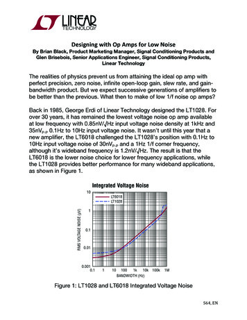
Transcription
Chapter 8NOISE, GAIN AND BANDWIDTH INANALOG DESIGNRobert G. MeyerDepartment of Electrical Engineering and Computer Sciences, University of CaliforniaTrade-offs between noise, gain and bandwidth are important issues in analogcircuit design. Noise performance is a primary concern when low-level signals must be amplified. Optimization of noise performance is a complex taskinvolving many parameters. The circuit designer must decide the basic form ofamplification required – whether current input, voltage input or an impedancematched input. Various parameters which can then be manipulated to optimizethe noise performance include device sizes and bias currents, device types (FETor bipolar), circuit topologies (Darlington, cascode, etc.) and circuit impedancelevels. The complexity of this situation is then further compounded when theissue of gain–bandwidth is included. A fundamental distinction to be madehere is between noise issues in wideband amplifier design versus narrowbandamplifier design. Wideband amplifiers generally have bandwidths of severaloctaves or more and may have to operate down to dc. This generally meansthat inductive elements cannot be used to enhance performance. By contrast,narrowband amplifiers may have bandwidths of as little as 10% or less of theircenter frequency, and inductors can be used to great advantage in trading gainfor bandwidth and also in improving the circuit noise performance. In order toexplore these issues and trade-offs, we begin first with a description of gain–bandwidth concepts as applied to both wideband and narrowband amplifiers,followed by a treatment of electronic circuit noise modeling. These conceptsare then used in combination to define the trade-offs in circuit design betweennoise, gain and bandwidth.8.1.Gain–Bandwidth ConceptsAll commonly used active devices in modern electronics are shown inFigure 8.1(a) and may be represented by the simple equivalent circuit shownin Figure 8.1(b). Thus the bipolar junction transistor (BJT), metal-oxidesemiconductor field-effect transistor (MOSFET), junction field-effect transistor(JFET) and the gallium arsenide field-effect transistor (GaAsFET) can all begeneralized to a voltage-controlled device whose small-signal output currentis related to the input control voltage by the transconductanceIn this227C. Toumazou et al. (eds), Trade-Offs in Analog Circuit Design: The Designer’s Companion, 227–256. 2002 Kluwer Academic Publishers. Printed in the Netherlands.
228Chapter 8simplified representation, the output signal is assumed to be a perfect currentsource and any series input resistance or shunt feedback capacitance is initiallyneglected. This enables us to focus first on the dominant gain- bandwidth limitations as they relate to noise performance. (Note thatfor the FETs.)The effective transit time of charge carriers traversing the active region of thedevice is [1]and the effective low-frequency current gain isAgain note thatfor the FETs. In this simple model neglecting parasiticcapacitance, we find that the frequency of unity small-signal current gain is [1]In order to obtain broadband amplification of signals we commonly connectamplifying devices in a cascade with load resistanceon each stage. Considera typical multistage amplifier as shown in Figure 8.2.The portion of Figure 8.2 enclosed in dotted lines can be considered arepetitive element that comprises the cascade. The gain of this element orstage is
Noise, Gain and Bandwidth in Analog Design229from which we see that the mid-band gain magnitude isand the – 3 dB bandwidth (rad/sec) isThus the gain–bandwidth product of this stage isThe importance of the device (or process for integrated circuits)is thusapparent. From (8.7) we can conclude that in a cascade we cannot achieve gainover a wider bandwidth than the device(excluding inductors) and that wecan trade-off gain against bandwidth by choosingThis process is calledresistive broadbanding. Wider bandwidth is achieved at the expense of lowergain by using low values ofThese conclusions also apply if the signalinput to the amplifier approximates a current source and the stage consideredis not part of a multi-stage amplifier but is an isolated single gain stage. Thisis the case, for example, in fiber-optic preamplifiers. However, if the signalsource to the amplifier approximates a voltage source, then the single-stagebandwidth (and thus the gain–bandwidth) is ideally infinite. This case is rarelyencountered in practice at high frequencies (gigahertz range), but may be foundin sub-gigahertz applications. More commonly at frequencies in the gigahertzrange, we find the first stage of an amplifier driven by a voltage source (e.g.coming from an antenna) in series with a resistive source impedance(often50 orIn that case the signal input can be represented by a Nortonequivalent current source in parallel withand the previous analysis is valid,ascan be lumped in with
2308.1.1.Chapter 8Gain–Bandwidth ShrinkageIf we construct a multi-stage amplifier consisting of N identical stages withresistive interstage loads as shown in Figure 8.2, we can describe the gain–bandwidth behavior of the amplifier as follows. If the gain per stage is G andthe bandwidth per stage is B then the overall amplifier transfer function for Nstage isThe overall – 3 dB frequency of the amplifier is the frequency whereFrom (8.8) this isThus, we see that the bandwidth shrinks as we add stages. For example,for N 2 andfor N 3. In an N-stageamplifier, the overall mid-band gain isand we can define a per-stagegain–bandwidth figure-of-merit asWe conclude that the cascading of stages each with a negative-real-pole transferfunction results in significant loss of gain–bandwidth product.Gain–bandwidth shrinkage is also caused by parasitic elements. The inclusion of parasitic capacitance in shunt withcauses a reduction of the deviceand consequent loss of gain–bandwidth. Thus, in wideband integrated circuit (IC) design, the layout must be carefully chosen to minimize parasiticcapacitance. Any resistance in series with the input lead (such as the baseresistance of a BJT) also causes loss of gain–bandwidth. Consider the cascade of Figure 8.2 with parasitic resistance added to each device as shownin Figure 8.3 whereis now neglected. Taking one section as shown in thedotted line, we findfrom which the mid-band gain isand the –3 dB bandwidth is
Noise, Gain and Bandwidth in Analog Design231Thus the gain–bandwidth product of the stage isWe see that the gain–bandwidth is reduced by the ratioThisleads to trade-offs in wideband design since we can reduce the magnitude ofby increasing the device size in the IC layout. This also reduces the noisecontribution from (to be considered later) which is highly desirable, but hasthe unwanted effect of increasing the parasitic device capacitance which leadsto a reduction ofand consequent loss of gain–bandwidth.Loss of gain–bandwidth also occurs in simple amplifier cascades due toMiller effect, although the loss becomes less severe asis reduced, whichis often the case for high-frequency wideband amplifiers. Consider the singleamplifier stage shown in Figure 8.4 where feedback capacitanceis included.(This represents the collector–base parasitic capacitance in BJTs and the drain–gate parasitic in FETs.)
232Chapter 8The Miller capacitance seen across the input terminals is [2]Thus, the total input capacitance isThe time constantcan be compared withto determine theloss of stage gain–bandwidth. The smallerthe less the effect. For example,ifandGHz, we findandIn this case, Miller effect reduces the stage gain–bandwidthby 10%. A trade-off occurs again if noise must be minimized by increasing thedevice size (to reducein that this will increaseand increase the Millereffect.8.1.2.Gain–Bandwidth Trade-Offs Using InductorsInductive elements have long been used to advantage in electronic amplifiers.Inductors can be used to obtain a frequency response which peaks in a narrowrange and thus tends to reject unwanted out-of-band signals. However, theadvantages of using inductors extend beyond this as they allow the inherentdevice gain–bandwidth to be arbitrarily moved across the spectrum, as willnow be shown. Consider the single-stage amplifier shown in Figure 8.5 andinitially neglect feedback capacitance. The input resistancerepresents thebasic device input resistance in shunt with any external resistors such as biasresistors. The stage transfer function isThe stage gain isand the – 3 dB bandwidth isgiving the stage gain–bandwidth product as
Noise, Gain and Bandwidth in Analog Design233as before. The frequency response given by (8.19) is plotted in Figure 8.6.Now consider adding a shunt inductor as shown in Figure 8.7. The transferfunction of the circuit of Figure 8.7 isAt resonance
234Chapter 8whereThe – 3 dB bandwidth of the transfer function iswhereFrom (8.25) and (8.26), we find the gain–bandwidth product of the circuitis nowas before. However, the gain is now realized in a narrow band centered on thefrequencyas shown in Figure 8.8.We can thus shift the high-gain region of the device transfer function to highfrequencies using the inductor. In practice, the existence of lossy parasiticssuch as reduces the gain at very high frequencies, but nonetheless we arestill able to trade-off gain for bandwidth quite effectively in this way. Typicalperformance is shown in Figure 8.9 where ideal lossless behavior is comparedwith typical practical results. High-frequency gain larger than the lowpassasymptote is readily achieved.8.2.Device Noise RepresentationIn order to examine trade-offs between noise performance and gain–bandwidth, we need a convenient means to compare the noise performanceof different devices and different configurations. This is best done by representing the active-device noise behavior by equivalent input noise voltage and
Noise, Gain and Bandwidth in Analog Design235current generators [3]. Although these generators are correlated in general, wefind in many applications that one or other generator is dominant and thus theother generator and the correlation can be neglected. Once again we begin withthe simple general representation of Figure 8.1 and add noise generators asshown in Figure 8.10(a) (white noise only is considered).We then calculate equivalent input generators which model the device noisebehavior as shown in Figure 8.10(b). In Figure 8.10(a), the output noise sourceis caused by thermal noise in FETs and shot noise in BJTs. Thus,
236Chapter 8for BJTs andfor FETs.The input noise generator can be assumed zero for FETs and for BJTs it iscaused by shot noise in the base current given byNote that if a physical shunt resistor R is connected in shunt with the deviceinput (e.g. due to bias circuits), then this can be folded into the noise representation by including it in(which becomesand adding a thermal noisegenerator to of valueThe equivalent input generators of Figure 8.10(b) now becomeandwhere the ac current gainof the device is given byThe expression for in (8.33) can be related to the device transconductancein general for any active device by usingfor BJTs and deriving:for FETs andfor BJTs. Finally, the representation of Figure 8.10(b) can be enhanced byadding to a thermal noise generator due to any physical series input resistancesuch as base resistance for BJTs, given by
Noise, Gain and Bandwidth in Analog Design237The equivalent input noise representation of Figure 8.10(b) can now be usedto generate some general conclusions regarding low-noise design before weexamine the specifics of the gain–bandwidth noise trade-off. For amplifiers inwhich the input noise current is important (such as fiber-optic amplifiers drivenby a high-impedance source), the noise is dominated byThus FETs have anadvantage in that there is no input shot noise contribution as in BJTs. However,both FETs and BJTs tend to be dominated in high-frequency wideband applications by the frequency-dependent second term in (8.34). At high frequencies,this asymptotes tofor all devices. Thus a high device becomes important as does minimizationofThis then involves trade-offs involving device bias point and dc powerdissipation. The use of low collector currentin BJTs can help the noiseperformance but may degrade the deviceIn the case of FETs the designerhas more degrees of freedom in that the FET transconductance depends on bothdrain bias currentand device geometry via W/L.For applications where the input noise voltage generatoris dominant(where the driving source impedance is low) all active devices are operatedwith the maximum possible transconductanceThis in general calls forhigh bias currents and large area devices with high W/L when using FETs.If BJTs are used, then high bias currents are also required to give a largevalue of gm , and in addition, the base resistance must be minimized which alsorequires large device area. The trade-offs here involve dc power dissipation andthe deleterious effects of increasing device parasitic capacitance as the activedevice area is increased.The issue of the impact of negative feedback on the noise-gain–bandwidthtrade-off will be discussed in a later section. However, at this point it is worthconsidering the impact of noise performance of the most common form offeedback-series resistive degeneration (local series feedback) in the common
238Chapter 8lead as shown in Figure 8.11, This connection can be used with all activedevices.It leads to improved linearity, facilitates the trade-off of gain for bandwidthand allows the manipulation of the device input and output impedances. However, there is a noise penalty in that the equivalent input noise voltage generatorof the circuit is increased by the amount of thermal noise inwhich isThe equivalent input noise current is unchanged. The gain of thecircuit as expressed by the transconductance is reduced by the negative feedbackdue toand is given byNote that the feedback loop gain in this circuit is8.2.1.Effect of Inductors on Noise PerformanceThe use of inductors to trade-off bandwidth versus gain was described above.Inductors also offer the opportunity to realize significantly improved noiseperformance in high-frequency amplifiers. This can be appreciated by addinga shunt inductor L as shown in Figure 8.7 across the input of the equivalentcircuits of Figure 8.10. Then at the parallel resonant frequency,the inductive and capacitive impedances cancel at the input of the device andthe frequency dependent term in in (8.34) disappears. This gives significantlyimproved noise performance in many high-frequency applications, although thetechnique is obviously restricted to narrowband circuits. Inductive optimizationof noise performance based on these principles is commonly implementedin gigahertz range narrowband low-noise amplifiers (LNAs) used in wirelesscommunication systems.Another common and important use of the inductors in high-frequencylow-noise circuits is in inductive common-lead degeneration as shown inFigure 8.12(a). The small-signal equivalent of this connection is shown inFigure 8.12(b), where a simplified active device equivalent has been used.In order to examine the effect ofon noise performance, the output noisegenerator is also included.First, we omitand examine the effect ofon the gain and inputimpedance of the stage. The major benefit ofis in boosting the resistive partof the input impedance of the stage without degrading the noise performance,as happens with resistive degeneration. The use of common-lead inductance iswidespread in LNA design using both FETs and BJTs, although once again thetechnique is limited to narrowband applications. The physical inductor is oftenrealized using the package bond wires [4], or on-chip spiral inductors can alsobe used [5–7]. By calculating the current flowing into the equivalent circuit
Noise, Gain and Bandwidth in Analog Design239of Figure 8.12(b), we find the input impedance isThis expression can be represented by the equivalent circuit of Figure 8.13.We see that a resistive portionappears which can be chosento have an appropriate value to allow matching to typical RF source resistances of 50 or 75This same result could be achieved by simply adding aphysical series input resistor, but this would add a large amount of noise tothe circuit and is generally an unacceptable option. Additional input inductive and capacitive elements are usually added to produce a purely resistiveexternal input impedance. Typical values in (8.42) might be
240Chapter 8andandThe introduction ofestimated fromgiving the resistive portion ofThis would correspond toa valuetypically causes a reduction in gain and this can beThe effect ofon noise performance is somewhat complicated, but a roughidea can be obtained by referring the noise generator in Figure 8.12(b) backto the input, giving an equivalent input noise voltage generatorWe see that the effect ofis to reduce the magnitude of compared to thecase whereis absent. In practice, we find small but useful improvementsin the noise performance of high-frequency LNAs when this technique is usedto help match the input. Forandwe find the factorto have values 0.96 (–0.2 dB) at 1 GHz and 0.67 (–1.7 dB) at3 GHz.8.3.Trade-Offs in Noise and Gain–BandwidthThe considerations described above focused on noise and gain–bandwidthrepresentation of electronic circuits. We now use these tools to examine issuesand methods of trade-off between these quantities.8.3.1.Methods of Trading Gain for Bandwidth and theAssociated Noise Performance Implications [8]The trade-off of gain for bandwidth can be achieved in a number of ways,with noise performance, terminal impedances and the form of the circuit transfer function being important constraints. The use of inductors to transfer thedevice gain to a higher frequency in narrowband applications has been treatedin Subsection 8.1.2 and will not be considered further. For broadband amplifiers, the simplest method of trading gain for bandwidth is the use of resistivebroadbanding as described in Section 8.1. This method has the advantage ofsimplicity, but has the drawbacks of gain–bandwidth shrinkage over multiple stages and limitations on control of the circuit terminal impedances. Forexample, if a resistive input impedance ofis required to match a sourceresistance ofthe only option available is connection of a shunt resistorto ground as shown in Figure 8.14. Assume the device input resistanceis large and let
241Noise, Gain and Bandwidth in Analog DesignWe can calculate the circuit noise figure by comparing the total noise atwith that due to the source resistance. The input impedance of the active devicedoes not affect the following noise figure calculation and is neglected. Usingwe find for the total noise atwhere correlation has been neglected. The noise atresistance isdue to the sourceFrom the definition of noise figure, we haveand using (8.45) and (8.46) in (8.47), we findIfis omitted from the calculation, the circuit noise figure isFrom (8.48) and (8.49), we see that for low-noise circuits, the degradation incircuit noise figure caused by the addition ofis about 3 dB and canbe higher. This is unacceptable in many applications.These limitations on simple resistive broadbanding lead us to examine otheroptions. One of the most widely used is negative feedback [9]. The basic
242Chapter 8trade-off of gain and bandwidth allowed by the use of negative feedback canbe illustrated by the following simple example. Consider an idealized negative feedback amplifier with a one-pole forward gain function as shown inFigure 8.15.The forward gain path has a transfer functionwhereThe gain versus frequency of the open and closed loop amplifier is shown inFigure 8.16 where f is assumed frequency independent.The gain of the feedback amplifier is
Noise, Gain and Bandwidth in Analog Design243where the loop gain isthe mid-band gain isand the – 3 dB frequency isFrom (8.52) and Figure 8.16, we see that the use of negative feedback allows adirect trade-off of gain for bandwidth while maintaining a fixed gain–bandwidthproduct.In addition to the gain–bandwidth trade-off, the use of feedback allowsmodification of the terminal impedance of the amplifier. If the forward gainblock has an input resistancethen shunt feedback at the input gives amodified (lowered) input resistanceSeries feedback at the input raises the input resistance toThe use of combined shunt and series feedback can give intermediate valuesof terminal impedances and this technique will be described below. The use ofcombined feedback allows realization of matched terminal impedances withmuch less noise-figure degradation than is caused by simple shunt or seriesresistive matching.8.3.2.The Use of Single-Stage Feedback for theNoise-Gain–Bandwidth Trade-OffConsider a cascade of local series feedback stages as shown in Figure 8.17.The active device with feedback resistorcan be represented by the simplifiedhigh-frequency equivalent circuit of Figure 8.18. If the loop gainis large, this equivalent circuit reduces to that shown in Figure 8.19, where theeffective transconductance is given byThe transconductancehas a pole with magnitudethat can usually beneglected. We see that the input capacitance and transconductance are both
244Chapter 8reduced by the factor (1 T). Thus using the analysis of Section 8.1, weconclude that gain and bandwidth can be traded off via the feedback resistorA significant advantage of this technique over simple resistive broadbanding isthe linearization produced byThe noise introduced byis described inSection 8.2. The device dc power dissipation is also part of this trade-off sinceandincreases as the bias current increases. This trade-off allowssmallerto be used for a given value of T with improved noise performance.Note that the input resistance of this stage is now quite large and will generallynot meetmatching requirements.Single-stage feedback can also be implemented in the form of shunt feedbackas shown in Figure 8.20. The shunt feedback stage has low input and outputimpedances and is not suitable for cascading. It can be used as a stand-alone single stage and if parasitic capacitances are neglected, we find the transimpedancegain is
Noise, Gain and Bandwidth in Analog Design245From (8.59), we see that the gain–bandwidth product isThus, gain and bandwidth can be traded using the value ofimpedance is given byThe inputThe input impedance is usually dominated by the last term in (8.61) and islow. Thus, this stage is well suited to current amplification and is often used inthat role.The noise performance of the shunt feedback stage of Figure 8.20 is easilyestimated by recognizing that a shunt feedback resistor such ascontributesto the equivalent input current noise generatorThus, as the stage is broadbanded by reducingthe equivalent input noisecurrent increases. This trade-off is well known to designers of high-speedwideband current amplifiers such as are used in fiber-optic receivers [10,11].
246Chapter 8The single-stage feedback circuits described above can be used in mismatched cascades to form wideband voltage or current amplifiers using twostages as shown in Figure 8.21 [12]. Transimpedance and transresistanceamplifiers can be implemented by adding additional stages. The advantageof the configurations of Figure 8.21 is the minimal interaction between stagesand the dependence of the gain solely on resistor ratios for large values of loopgain T.The single-stage feedback amplifiers considered so far do not allow realization of low-noise wideband matched-impedance amplifiers. This function can,however, be achieved by appropriate use of multiple feedback loops. Considera single-stage dual-feedback amplifier as shown in Figure 8.22. We assume
247Noise, Gain and Bandwidth in Analog DesignIfandthe input impedance can be approximated bya parallel RC combination with valuesThe output resistance is approximatelyand we findifIn a matched amplifier we setThe gain is then given byThe – 3 dB bandwidth is set by the time constant oflevel at the input node) givingand(the impedanceThus the gain–bandwidth of the stage isusing (8.63), (8.66) and (8.67). We can thus realize a matched impedanceamplifier and trade gain for bandwidth using resistor values.The advantages of the circuit of Figure 8.22 are further evident when weexamine the noise performance. If the basic active device has equivalent inputnoise generators andthen the addition of resistorsandmodifythese toThe noise figure of the amplifier can now be calculated as
248Chapter 8We see that the noise figure is degraded by an additive factor ofand this can be made a reasonably small contribution. For example, ifandthen the amplifier gain is G 5,bandwidthandIf the basic device noisefigure is 2 dB (8.58), then the overall amplifier noise figure is 1.58 0.2 1.78which is 2.5 dB. The addition of the matching resistors has only degraded thedevice noise figure by 0.5 dB.8.3.3.Use of Multi-Stage Feedback to Trade-Off Gain,Bandwidth and Noise PerformanceThe single-stage feedback circuits described above are widely used in practice because of their ease of design and good overall performance. However,higher levels of performance can be achieved (higher gain and bandwidth andlower noise) if we allow use of feedback over multiple stages. The price paidfor this improved performance is increased complexity of design and, in particular, the possibility of oscillation [13] which must be addressed by appropriatecircuit compensation.Consider the two-stage shunt–series feedback amplifier in Figure 8.23[9–11,14,15]. This circuit has low input impedance, high output impedanceand a well-stabilized current gain given byfor high loop gain. This is called a current-feedback pair.The gain–bandwidth trade-off in this circuit can be calculated from the smallsignal equivalent circuit of Figure 8.24. The feedback current is given byThe feedback loading on the input isand this is lumped in withto formThe input resistance and capacitance of the second stage are
Noise, Gain and Bandwidth in Analog Designand249respectively and are given byandforResistorsandare lumped to formFeedbackcapacitorincludes the inherent feedback capacitance of the input deviceplus any added capacitance used for frequency compensation.The forward path gain function of the amplifier is [2]IfandthenandNote that asis made larger, the dominant poledecreasesin magnitude andincreases while the productis constant.
250Chapter 8The frequency response of the circuit can be estimated using the rootlocus [13] of Figure 8.25. As the loop gain is increased from zero, the polesof the circuit transfer function come together and then split out in the s -plane.We assume the loop gain is adjusted to give pole positions as shown at AA atangles of 45 to the real axis. This gives a maximally flat frequency response(no peaking) and a circuit – 3 dB bandwidth equal to the distance from A tothe origin. Ifthis isThus the bandwidth of the circuit isThese pole positions give the maximum possible gain–bandwidth without peaking and are set by manipulating the loop gain and the compensation capacitorNote that a similar compensation function can be achieved by a capacitorconnected acrossThe loop gain required to set the poles in the positionAA is [13]The mid-band forward gain (current gain)From (8.80), we haveis given by
Noise, Gain and Bandwidth in Analog Design251wherehas been used. In practice, parasiticcapacitance shuntingat the internal node will cause a degradation of devicefrequency capability and (8.84) becomeswhereis theeffective value ofwhich is realized in practice with parasitic capacitanceincluded.The mid-band forward gain of the circuit (current gain) with feedbackapplied isSubstituting (8.84) and (8.82) in (8.86), we findUsing the multistage gain–bandwidth figure-of-merit defined in (8.10), we findusing (8.88) and (8.81). Thus, for this two-stage feedback connection, the fulldevice gain–bandwidth per stage is preserved. This is a significant advantagewhen compared to the gain–bandwidth shrinkage experienced in a cascade oftwo single stages.The noise performance of the two-stage amplifier is simply that of the amplifier input device with the addition of thermal noisedue tothe feedback resistor. However, due to the extra gain–bandwidth available inthe two-stage configuration compared with a single-stage cascade, we find thatlarger values ofcan be used in the two-stage amplifier, giving improvednoise performance. It should also be noted that the compensation capacitordoes not appreciably degrade the circuit noise performance as long asA two-stage feedback voltage amplifier can be realized using the series–shunt configuration of Figure 8.26. The series feedback at the input gives thestage a high input impedance while the shunt feedback at the output producesa low output impedance. For large loop gain, the overall voltage gain is set by
252Chapter 8resistor ratios and isIfthe gain–bandwidth product is again given by (8.89), where G isnow the amplifier voltage gain. In this case, the noise performance is that ofthe input device with an addition ofto the equivalent inputnoise voltage.Finally, in the realm of two-stage feedback amplifiers, we examine the twostage dual-feedback amplifier shown in Figure 8.27 [16–19]. This is derived byanalogy and extension from the single-stage version in Figure 8.22 and incorporates both series–shunt and shunt–series feedback loops. Like the single-stageversion of Figure 8.22, the circuit of Figure 8.27 gives excellent gain–bandwidthperformance while simultaneously allowing realization of matched terminalimpedances with good noise performance. A simplified small-signal equivalentcircuit of the amplifier in Figure 8.27 is shown in Figure 8.28 where
Noise, Gain and Bandwidth in Analog Design253andThe circuit of Figure 8.28 can be manipulated into the e
ANALOG DESIGN Robert G. Meyer Department of Electrical Engineering and Computer Sciences, University of California Trade-offs between noise, gain and bandwidth are important issues in analog circuit design. Noise performance is a primary concern when low-level sig-nals must be ampli