Transcription
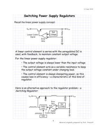
13 Sept 2010Switching Power Supply RegulatorsRecall the linear power supply concept:A linear control element is series with the unregulated DC isused, with feedback, to maintain constant output voltage.For the linear power supply regulator: The output voltage is always lower than the input voltage The control element acts as a variable resistance to keepthe output voltage constant under changing load. The control element is always dissipating power, so thiscauses loss in efficiency – a characteristic of this kind ofregulator.Here is an alternative approach to the regulator problem – aSwitching Regulator:1Material originally prepared by Prof. Prescott
13 Sept 2010Switching regulators operate by rapidly switching the pass transistorbetween two efficient operating states:1. Cutoff – where there is a high voltage across the passtransistor, but no current flow.2. Saturation – where there is a high current through thepass transistor, but a very small voltage drop.Characteristics of Switching Power Supplies: Since the control element is either on or off, there is littlepower dissipation. Can generate output voltages higher than the unregulated input. Can generate output voltages of opposite in polarity to theinput. Can be smaller and lighter weight than a linear PS regulator. Problem: NOISY and Complex to buildMany applications require both types to be used. For example, aswitching regulator may provide the initial regulation, then a linearregulator may provide post-regulation for a noise sensitive part of thecircuit, such as a sensor interface or A/D converter.Here is a comparison of linear versus switching power supplies2Material originally prepared by Prof. Prescott
13 Sept 2010The switching power supply is an improvement (in many ways) overthe linear power supply. Here is the concept:Switching Power Supply Block DiagramHere are the essential waveforms that describe the operation ofthis system.loadcurrentSwitching and Control Waveforms3Material originally prepared by Prof. Prescott
13 Sept 2010Before going further, let’s review how inductors charge anddischarge.recall:VL L di t dt L I TSwitched Inductor ActionThere are three types of switching power supplies:1. Step down regulator – sometimes called a “buck” regulator.2. Step up regulator – sometimes called a “boost” regulator.3. Inverting regulator – sometimes called a “flyback” regulator.In Project #2 we will focus on buck and boost regulator design.4Material originally prepared by Prof. Prescott
13 Sept 2010Here’s a closer look at the control element, plus capacitor andinductor, showing how these are configured for the three types ofregulators:Diode D1 is oftencalled the “catch”diode. It is usuallya Schottky-barrierdiode, having lowforward voltagedrop and fastswitching speed.Make sure youunderstand theprinciples describedby these diagrams5Material originally prepared by Prof. Prescott
13 Sept 2010Step-Down Switching Regulatortoff Let’s analyze this circuit and learn how it works:1. The filter averages the voltage square waves which are created by switchingVin on and off. The filter averages these waveforms to produce a dc voltage.Vo Vin tontonVin T ton toffduty cycle2. When Q1 switches ON, the inductor charging current is:IL VL V V Vt in sat oLL t Vsat is the voltage dropped across Q1 when it is saturated.3. When Q1 switches OFF, the inductor current is: V VD1 I L I L ( peak ) ot L 6 See and on thenext pageMaterial originally prepared by Prof. Prescott
13 Sept 2010A closer look at the waveforms in this system:Vin VD1Voltage acrossswitch Q1VinVsatVoltage acrossDiode D1Vin VsatVinVD1I pkSwitch CurrentQ1I in I C ( Avg )I pkDiode D1CurrentI D1( Avg )Inductor CurrentIo I pk2I pk I C ( Avg ) I D1( Avg )tofftonTCapacitorCurrent I pk 212 I pk 2 I pk 2CapacitorRipple VoltageVo V pkVoVripple ( p p )Vo V pkton 2 toff 27Material originally prepared by Prof. Prescott
13 Sept 2010Here’s how to configure the switching regulator for step-up andinverting operation.8Material originally prepared by Prof. Prescott
13 Sept 2010Now look at the components of the control circuitry9Material originally prepared by Prof. Prescott
13 Sept 2010Tying it all together, we have the following step-down switcherThe control circuitry can be implemented using individual devices oryou can make use of an integrate controller such as the 74S40, asshown below.However, we will not use a device such as this. Instead we willimplement the functions using a 723 and a dual 555 timer.10Material originally prepared by Prof. Prescott
13 Sept 2010Here is a schematic of the way we will implement a switching powersupply for Project #2.11Material originally prepared by Prof. Prescott
13 Sept 2010It is critically important that you have a complete understanding ofhow this circuit operates before you try to build it. You must alsounderstand how the 723 and 555/556 devices function.Now let’s look at some design considerations. There are threeprimary subcomponents to this project. They are:1. The control element and charging circuitryThis schematic shows the TIP-42 used as the control element. Youare not constrained to using a PNP device here. You can alsoinvestigate the use of the TIP-41, which is an NPN transistor. Youalso might want to try using a power field-effect device. Try theIRF511.IRF-511TIP-41What is necessaryfor the 556 todrive this device?Is it much easier touse than a BJT?Can the 556provide sufficientdrive current touse this kind ofimplementation?12Material originally prepared by Prof. Prescott
13 Sept 20102. The oscillator and pulse width modulatorCPulse-Width ModulatorB(bi-stable mutivibrator)AOscillator(astable multivibrator)(20 kHz – 100 kHz)13Material originally prepared by Prof. Prescott
13 Sept 20103. The voltage sensor and error amplifierHere we have the familiar723 – you shouldunderstand all about thisdevice at this point.BError voltage output tothe PWMOutput voltage is sensed hereIn this application, the 723 is operating in a circuit that has anoutput voltage that is lower than the internal reference voltage.Recall this diagram from Project #1:maybe you should use one ofthese?14Material originally prepared by Prof. Prescott
13 Sept 2010Design Steps for the Step Down Switching RegulatorHere are some suggested steps to designing the output circuitry for theswitching regulator. These are to be used as guidelines to get you in theballpark. Use these in conjunction with the document entitled “Step DownSwitching Regulator Operation & Design.” Don’t hesitate to experiment –there is plenty of latitude in the design.Step #1 – State your “givens”VIN DC input voltageVOUT DC output voltageI OUT max Maximum load currentVD1 Forward voltage of catch diodeVsat Saturation voltage of switching transistorVripple(p-p) Peak-to-peak ripple ( 0.5%)Step #2 – Determine the peak output currentI L ( pk ) 2 I OUTStep #3 – Determine the ratio of on/off time for the switching transistortonVOUT VD1 toff VIN Vsat VOUTStep #4 – Select a switching frequencySelect a frequency within the following range:30,000 Hz f 60,000 Hzand note that: f 1ton toff15Material originally prepared by Prof. Prescott
13 Sept 2010Step #5 – Calculate the value for the switching inductorLmin VIN Vsat VOUTtonI pk ( switch )Step #6 – Calculate the value for the switching capacitorCO I pk ( switch ) ton toff 8 Vripple ( p p )Step #7 – Determine the regulator efficiency VOUT VIN Vsat VD1 VVVIN D1 OUT 16Material originally prepared by Prof. Prescott
13 Sept 2010The 555 Integrated Circuit Timer Operates from a wide range of power supplies(see H & H p. 289) Timing intervals of several minutes. Frequenciesas high as a few MHzRemember how the comparator functions: - - - -17-Material originally prepared by Prof. Prescott
13 Sept 2010Summary of Operation:Three 5 k resistors are configured in series to divide Vcc intothirds. The junctions of these resistors are tied to comparators.This serves as a constant reference voltage that is only dependentupon Vcc.To force the output of the 555 low, the voltage on the “Threshold”input must exceed 2/3 Vcc. This also turns the dischargetransistor “on”. To force the output of the timer high, the voltageon the “Trigger” input must fall below 1/3 Vcc. This also turns thedischarge transistor “off”.The diagram on the previous page shows the 555 connected in freerunning (astable) mode.We can design the 555 to operate at a specific free-running rate bychoosing Ra, Rb and C. Let’s examine how this is accomplished.t RCV t A 1 e You might recall that:defines the charging of an general series RC circuit.1. Time to charge2V t VCC3A VCCR RA RB20 VCC3t 2RCVCC VCC 1 e 3 e tRC 13so18t 1.09 RCMaterial originally prepared by Prof. Prescott
13 Sept 2010132. Time to charge 0 VCCt 1VCC VCC 1 e RC 3 t 0.405 RC3. Time to charge12VCC VCC33thigh 1.09 RC 0.405 RC 0.69 RCthigh 0.69 RA RB CThe next thing we need to do is look at the discharge behavior ofthe RC circuit. Note that the discharge of an RC circuit is definedas:V t Ae4. Time to discharge tRC21VCC VCC33t 12RCVCC VCC e33But here, R RBbecause of thedischarge path.tlow 0.69 RB C19Material originally prepared by Prof. Prescott
13 Sept 20105. Finally, the period of the output signal is:T thigh tlow 0.69 RA RB C 0.69 RB C 0.69 RA 2 RB Calsof 11.45 T RA 2 RB C20Material originally prepared by Prof. Prescott
13 Sept 201021Material originally prepared by Prof. Prescott
13 Sept 2010Winding the InductorThe inductor will be hand-wound using the Ferroxcube 2213PA5003C8. These are ferrite inductor cores that are snapped around aplastic bobbin on which is wound the coil. Since the wire is wound ona bobbin rather than around the ferrite material itself, it is easy tochange bobbins and experiment with the various inductancesproduced by different numbers of turns and kinds of wire.Two features of this core: This core is a manganese-zinc ferrite substance withmedium permeability and low losses. It is designed specifically for high flux-density applicationssuch as power supplies.22Material originally prepared by Prof. Prescott
13 Sept 2010The inductance of a coil can be determined from the followingequation:N 2 A r oL where:L Inductance in HenriesN number of turnsA Cross sectional area of coil (m2) r relative permeability of core material permeability of air (1.26 x 10⁻⁸) H/mℓ avg. coil length (m)You can use this information and the data in the Ferroxcube datasheet to determine the number of turns needs for a giveninductance. A shortcut is to use the following formula:N where:L 109ALN number of turnsL desired inductance in henriesAL millihenries/1000 turns ( 500 for the3C8 core)To produce a 275 microhenry inductor, approximately23 turns are required. The result is not exact, so youwill have to experiment with it.23Material originally prepared by Prof. Prescott
13 Sept 2010Tips for success:1.Understand how step-down switching regulators work. Refer to H&H (Sect.6.19) and the reference material posted on the JEDL web site.2.Understand how the 555 functions and how to select components to makeit function predictably as an astable and monostable circuit. The 556 isjust two 555’s in one package. There is reference information on using the555 posted on the web site.3.Understand how the 723 operates in the application. It is used differentlythan in the previous project.4.Read the note entitled “Step-Down Switching Regulator Operation andDesign.” This is your primary source of information for this project.5.Break the circuit into three parts: Error amplifier (723), oscillator and PWM(556), and the output circuitry. Allow one person to focus on one of theseso that there is sufficient effort from all team members.6.Breadboard parts of the circuit just to get familiar with it. In the process youshould learn to wind and test the inductor. Play around with it andunderstand what happens when you change the peripheral components.7.Implement a Spice simulation of the pass transistor, diode, inductor andoutput capacitor. The purpose of this is to see how to bias the transistorand to make sure it switches properly. Also this is a check on the inductor8.Construct the completed circuit and test it. When testing the circuit,always keep a load on the circuit – it doesn’t function well without a load.Try to keep a minimum load of about 200 mA on the circuit when testing.24Material originally prepared by Prof. Prescott
The switching power supply is an improvement (in many ways) over the linear power supply. Here is the concept: Here are the essential waveforms that describe the operation of this system. load current Switching Power Supp