Transcription
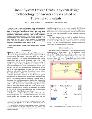
Circuit System Design Cards: a system designmethodology for circuits courses based onThévenin equivalentsNeil E. Cotter, Member, IEEE, and Cynthia Furse, Fellow, IEEEAbstract—The Circuit System Design cards described hereallow students to design complete circuits with sensors and opamps by laying down a sequence of cards. The cards teachstudents several important concepts: system design, Thevéninequivalents, input/output resistance, and op-amp formulas.Students may design circuits by viewing them as combinations ofsystem building blocks portrayed on one side of the cards. Theother side of each card shows a circuit schematic for the buildingblock. Thevénin equivalents are the crucial ingredient in tyingthe circuits to the building blocks and vice versa.Index Terms—Linear, circuit, system design, cards, ThevéninequivalentTI INTRODUCTIONHE deck of 32 Circuit System Design (CSD) cards allowsusers to design complete circuits by laying down cards insequence from left-to-right. The cards have two sides: asystem design side (with red-hatched surrounding and yellowbackground) and a circuit schematic side (with whitebackground). On the system design side, the processing ofsignals is represented by mathematical operations such asaddition or multiplication, or by logic operations such as ANDand OR. The user may design a system using only the systemside of the cards and then flip the cards over to see the circuitschematic and detailed formulas for deriving resistor valuesthat will yield desired additive factors and gains.Ideally, the transfer function of each block in a systemdesign would be independent of the preceding and succeedingblocks. For circuits, however, connecting a second block tothe output of a first block may cause loading that changes theoutput voltage of the first block. A unique feature of the CSDcards is that they account for these loading effects whileretaining the system design motif. For linear system design,the CSD cards give exact formulas for calculating the voltagesin a system in the presence of loading, and the calculationproceeds left-to-right, like the system design.The key idea underlying the design of the CSD cards is theThévenin equivalent, i.e., a circuit model consisting of a seriesvoltage source and resistance, and the realization that theN. E. Cotter is with the Electrical and Computer Engineering Dept.,University of Utah, Salt Lake City, UT 84112 USA (phone 801-581-8566, email: necotter@ece.utah.edu).C. Furse is with the Department of Electrical and Computer Engineering,University of Utah, Salt Lake City, UT 84112-9206 USA and also withLiveWire Test Labs, Inc., Salt Lake City, UT 84117 USA (e-mail:cfurse@ece.utah.edu).signal being processed in the system design is the Théveninequivalent voltage rather than the circuit output voltage per se.Furthermore, the Thévenin equivalent may be extended fromone card to the next, moving left-to-right, with pre-calculatedformulas.This paper discusses how the cards are used and the theoryon which they are based. The next section discusses one cardin detail, and the following section discusses a two-cardsystem. The final sections catalog the symbols incorporatedon the cards and the entire set of card images.II ONE-CARD EXAMPLEOne side of each CSD card shows a system view of how thecard processes its input signal. Fig. 1(a) shows the systemside of the Voltage Reference card that produces an outputvoltage, vTh, from a power supply voltage, VCC. Fig. 1(b)shows the circuit side of the Voltage Reference card with thecircuit diagram and formulas in terms of resistor values.(a)(b)Fig. 1. Voltage Reference card. (a) System side, (b) Circuit side.
As the system side of the card (with yellow background andread margin) shows, the input voltage, VCC, is scaled bygain, G. The formula for the Thévenin equivalent outputvoltage, vTh, is shown next to the output and represents thesystem output value.vTh GVCC(1)The arrow through the multiplier indicates that the gain isadjustable (by a potentiometer on the other side).The symbols in the right margin indicate how cards interact.The black arrow on the output line indicates that the gain onthis card is adjustable. The card also has the beginning of alarge red arrow with a smaller arrow through it in the rightmargin.red. This marking indicates that the Thévenin outputresistance is significantly larger than zero and may affect thegain of the next card, (if the input resistance for that card istoo low). If the next card has a low input resistance, the baseof the red arrow will be continued on the next card to form acomplete red arrow. In that case, the Thévenin equivalentresistance will have to be taken into account in the systemresponse.On the circuit side of the Voltage Reference card, theformula for the Thévenin equivalent output resistance isshown near the right edge.RTh Ra Rb(2)where the parallel operator, , is used as a shorthand for thecalculation of parallel resistance:Ra Rb (Ra 1 Rb 1 ) 1(3)The formula for gain G, found in the upper left, is revealedto be the voltage divider ratio of resistors.G RbRa Rb(4)Resistors Ra and Rb, constituting the potentiometer resistance,R, affect both the gain, G, and the Thévenin output resistance,RTh. A change in the Thévenin output resistance may changethe behavior of the next card.Note that the entire Voltage Reference card is equivalent toa voltage source of value vTh in series with a resistance ofvalue RTh, although the Thévenin equivalent circuit is notexplicitly shown. By itself, the Voltage Reference card tellsthe user how to convert the voltage divider circuit into itsThévenin equivalent, making it a useful reference tool.However, the cards become even more powerful when thesystem design is extended by appending cards on the right.III TWO-CARD EXAMPLEFig. 2 shows a two-card system design for a negativevoltage-reference circuit with low output resistance. On thesystem side of the cards, the Thévenin output voltage of thefirst card (on the left) is the input of the second card (on theright). The input of the second card is denoted as vTh . The" " symbol in the subscript means "from the card to the left".The transfer function for the entire system is found bycalculating the transfer functions from left-to-right. Theoutput of the first card is given in (1) above. Thus, our inputto the second card is given by (5).(a)(b)Fig. 2. Two-card system design for negative-voltage-reference circuit with low output resistance. (a) System side, (b) Circuit side.
vTh GVCC(5)The gain, G, listed in (4) and repeated here is given on thecircuit side of the first card.G RbRa Rb(6)The second card multiplies the value in (6) by a secondgain, also denoted by G, yielding the output value of the entiresystem.vTh GvTh GRbVCCRa Rb(7)(a)The gain, G, shown on the system side of the second carddepends on the Thévenin resistance of the first card, asindicated by the large red arrow in the margins between thecards and the small red line and arrow passing through themultiplier on the second card.The formula for G shown on the circuit side of the secondcard shows the dependence on the Thévenin resistance of thefirst card, the latter being denoted by RTh , which is given by(2). Using (2), we have the gain formula in (8) for the secondcard.G RfRs RTh RfRs Ra Rb(b)(8)Fig. 3. Op-Amp Buffer (V-Follower) card.(a) System side, (b) Circuit side.Substituting (8) into (7) yields the formula for the entirecircuit's Thévenin equivalent output voltage.Rf Rb vTh VCC Rs Ra Rb Ra Rb IV CARD SYMBOLS AND NOTATIONA. Overview(9)The designer is now free to choose values for resistors toachieve a desired output value for a given power supplyvoltage, VCC. Since the gains depend on ratios of values,which is typically the case with op-amp circuits, answers arenon-unique. The designer must choose practical resistorvalues that limit currents and noise to reasonable values.Values from 10 kΩ to 1 MΩ are work satisfactorily for opamp circuits.A final note on the system design is that the Théveninoutput resistance is approximately zero since op-amps havelow output resistance. The circuit side of the second cardexplicitly lists the Thévenin output resistance asapproximately zero. The system side of the second cardindicates the Thévenin output resistance is approximately zeroby having a white (or blank) box in the right margin. Thepresence of a blank box on either the input side (highresistance) or the output side (low resistance) breaks the chainof dependence of gains on previous cards.In other words, the blank box blocks arrows and means theRTh value from the previous card may be ignored. Cardsmay then be treated as independent steps in the system design,dramatically simplifying designs. For introductory op-ampdesigns, students may insert an Op-Amp Buffer (V-Follower)card, shown in Fig. 3, between circuit stages to blockThévenin resistance dependencies.Fig. 4 shows features on the circuit side of a card, and Fig. 5shows features on the system side of a card. The followingsubsections describe variations in the features.B. Card Suits and NumbersCSD cards come in four suits: Wire ( ), Component ( ),Amplifier ( ), and Gate( ). Suits may also be abbreviatedas the first letters: W, C, A, and G respectively. With theexception of the "W", these are the same letters as appear inthe base pairs of DNA. The authors have avoided thetemptation to promote this analogy, however.C. Notation for Recursive Thévenin Equivalent v and iAs noted above, the " " symbol means "from the card to theleft". When there are two inputs to a card, a "1" or "2"subscript is added, and the Thévenin equivalent voltage inputsare labeled on both sides of the card. The correspondingThévenin equivalent resistances also have a "1" or "2"subscript.D. Using Multiple RowsWhen cards have two inputs, the second input comes frombelow, implying that circuits may have more than one row.The right-angle wire card is used to bring the signal in fromthe bottom. A system could also have more than two rows,but another wire card from a second set of cards would berequired.
Fig. 4. Circuit System Design card circuit-side elements.Fig. 5. Circuit System Design card system-side elements.E. Calculating Transfer Functions Given Gain ConstraintsOne challenge for students is determining which cards canprovide a given gain formula, especially with two inputs. Thechallenge arises from the constraints on gains that are listed onthe system side of the cards. Students may be given transferfunction problems that involve only the system side of thecards, which separates the mathematical system problem fromthe circuit design problem.All gains on cards are positive numbers. Negative gains areindicated by adding a minus sign in front of the gain on thesystem side of the card.F. Large Arrows and Boxes in MarginsOn the system side of the card, arrows or boxes in themargin indicate interactions between cards that affect gains,owing to Thévenin equivalent resistances. The meanings ofthe arrows and boxes is as follows:1) large red arrow formed by adjacent cards interaction.2) red box interaction from previous card is forwarded tonext card, possibly completing a large red arrow overthree cards.3) white box interaction from previous card is blocked, sogains are determined only by the circuit on the carditself.G. Arrows for variable gainsRed arrows on the input side of a card lead to small redlines and arrows that indicate which gains on a card areaffected by which Thévenin equivalent resistances of previouscards.H. Op-Amp Differential Amp FormulationThe Op-Amp Differential Amp card allows for analysis ofcircuits with mismatched input voltage dividers. Normally,the input voltage dividers will be matched, and the systempath shown in gray for the E (for error) signal will be zero.Nevertheless, the E term is available if error analysis isdesired.
I. Black arrows in margin on output wiresBlack arrows on output wires indicate a variable outputarising from the presence of a potentiometer on the card.Changing the output voltage may also change the Théveninequivalent resistance.J. Component picture in lower left on circuit sideTo help beginning students understand circuits they buildon breadboards, pictures of the primary component on eachcard is shown in the lower left-hand corner on the circuit side.Though small, the component pictures of integrated circuitsalso show pin numbers.K. How to print and cut cardsThe Adobe Illustrator file for the cards is set up forprinting eight two-sided cards on a page. By turning layers onor off, pages may be printed from Illustrator itself. The toplayer in the file contains instructions for printing.A small set of eight cards may be used for covering just opamps. These cards are useful as references for the varioustypes of op-amp amplifiers.The outer box on the circuit side of the cards serves as a cutline. The wide, red, hatched margin on the system side isintentionally made larger than necessary to allow for amismatch in the registration of the images on the two side ofthe cards.L. Assembly and use of Level-shifter CardThe Op-Amp Level Shifter can translate low and high inputvoltages into different low and high output voltages. Thecomplexity of the equations for the level shifter necessitatedthe use of two cards. The two cards may be taped on one edgeto create a single hinged card that swings open to reveal theequations for the level shifter design. The suit and number aredimmed on the sides of the level shifter cards that go on theinside when the level shifter card is closed.V CONCLUSIONThe CSD cards allow the user to design simple circuitsystems by laying down cards from left to right representingcommon circuit building blocks such as voltage sources,resistors, op-amps, logic gates, and LED's. On the systemside, the cards show Thevenin equivalent voltages beingaltered by additions and multiplications to create a final outpu
on which they are based. The next section discusses one card followingsection discusses a two-card system. The final sections catalog the symbols incorporated on the cards and the entire set of card images. II ONE-CARD EXAMPLE One side of each CSD card shows a system view of how the card processes its input signal. Fig. 1(a) shows the system side of the Voltage Reference card that