Transcription
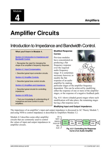
Module4AmplifiersAmplifier CircuitsIntroduction to Impedance and Bandwidth Control.What you’ll learn in Module 4.Modified ResponseCurvesSection 4.0 Introduction to Impedance andBandwidth Control.Previous moduleshave concentrated onproducing a flatfrequency responseover the requiredaudio frequencyrange. It is sometimesnecessary however, tomodify the flatresponse of an audioamplifier by makingparticular stages of the amplifier frequencydependent. This can be achieved by modifyingeither the response of one or more of the amplifierstages, or the response of a negative feedback path. Recognise the need for changing theshape of an amplifier’s frequency response.Section 4.1 Input Compensation. Describe typical input correction circuits.Section 4.2 Amplifier Controls. Describe typical tone control circuits.Section 4.3 Amplifiers and Impedance. Describe typical circuits for controllingimpedance.Section 4.4 NFB Quiz.Fig. 4.0.1 shows (shaded green) stages where suchmodification will take place, the remaining stageshaving a flat response curve. Test your knowledge & understanding ofimpedance and tone control in audioamplifiers.Modifying Input and Output Impedance.The importance of an amplifier’s input and output impedance is discussed in AC Theory Module 7,and using NFB to control impedance is described in Amplifiers Module 3.2.Module 4.3 describes some other amplifiercircuits that are commonly used to controlthe values of input and output impedances inamplifier circuits.Fig. 4.0.1 Controlling the ResponseCurve of an Audio AmplifierAMPLIFIERS MODULE 04.PDF1 E. COATES 2007 -2012
www.learnabout-electronics.orgAmplifier CircuitsModule 4.1Amplifier Input CompensationWhat you’ll learn in Module 4.1After studying this section, you should beable to:Recognise the need for changing the shape ofan amplifier’s frequency response.Understand the operation of typical circuits for: Input Compensation. Line Level. Phono De-emphasis.Input CompensationPre amplifiers are designed to increase the signal voltage amplitude of input devices to a levelsuitable for the input to a power amplifier. Pre-amplifiers often need a number of different inputs,each with a different gain and/or different input impedance. This is to ensure that each deviceconnected to the various inputs provides (after pre-amplification) an output level sufficient to drivethe input of a power amplifier and provide full power (when full volume is used) and minimumnoise.Line LevelThis pre amplifier output is usually called‘Line level’ and most amplifiers will havea line in and a line out socket, on PC soundcards these are normally coloured palegreen and light blue respectively. Theactual line level measured in volts variesbetween different types of equipment but isaround 1Vpp on consumer equipment to2.5Vpp on professional equipment. Withsome input devices such as CDs or radiotuners, little or no pre-amplification isneeded but devices such as microphones,phono inputs and guitar pickups providemuch lower signal levels and needspecially adapted inputs to the preamplifier.Fig. 4.1.1 Two Stage Pre-amp withInput CompensationAMPLIFIERS MODULE 04.PDF2 E. COATES 2007 - 2012
www.learnabout-electronics.orgAmplifier CircuitsPhono InputsInputs for phono cartridges used for playing legacy vinyl discs have an output of only a fewmillivolts and so need substantial amplification to reach line level. They also need the frequencyresponse to be modified, due to the ‘pre-emphasis’ applied to these discs during recording.Fig. 4.1.1 shows a two stage pre-amplifier circuit in which the negative feedback is applied viaresistors selected by the input selector switch, allowing different gain levels to be set by choosingone of three resistors (R7, R8 or R9) which will form a potential divider with R3 to set the gain.R9 (selected in the ‘phono’ position of SW1) also has capacitors connected in series and in parallelwith it to form a frequency selective network. The phono input is designed to accept a low levelinput from a record pick up.RIAA Pre-emphasisVinyl discs recorded to the RIAA (Recording Industry Association of America) standard have thehigh frequency end of their spectrum excessively amplified during the recording process and thelower frequencies reduced in amplitude. This has two main beneficial effects, firstly amplifying thehigher frequencies gives a significant improvement in the signal to noise ratio. Vinyl discs are proneto surface noise in the form of a high frequency hiss; increasing the signal amplitude of the higherfrequencies during recording makes the HF signal much louder than the hiss, then reducing theamplitude of the boosted high frequencies (the signal along with the hiss) back to a ‘normal’ levelduring playback, restores a level frequency response at the same time as reducing the hiss to a muchlower level, greatly reducing the apparent surface noise.A second advantage of reducing the amplitude of the lower frequencies during the recording ofvinyl discs, is that it reduces the amount of side-to-side movement required by the groove-cuttingstylus and so makes a narrower groove, this allows more information to be recorded on the samediameter disc.The result of this pre-emphasis is the standardRIAA curve shown in Fig. 4.1.2. This curvegoverns the amount of pre-emphasis appliedand so requires the amplifier to have a similarbut opposite sloping ‘de-emphasis’ curve toproduce a flat response.Fig. 4.1.2 RIAA Pre-Emphasis CurveAMPLIFIERS MODULE 04.PDF3 E. COATES 2007 - 2012
www.learnabout-electronics.orgAmplifier CircuitsModule 4.2Amplifier ControlsWhat you’ll learn in Module 4.2After studying this section, you should beable to:Understand typical circuits used for tonecontrol in audio amplifiers. Tone Control. Passive Bass - Treble Control. Active Bass - Treble Control. IC control of common amplifier functions.Tone ControlTone Control, shown in its most basic form in Fig. 4.2.1 providesa simple means of regulating the amount of higher frequenciespresent in the output signal fed to the loudspeakers. a simplemethod of achieving this is to place a variable CR networkbetween the voltage amplifier and the power amplifier stages,The value of C1 is chosen to pass the higher audio frequencies,this has the effect of progressively reducing the higherfrequencies as the variable resistor slider is adjusted towards thebottom end of the tone control, The minimum level of attenuationof the higher (treble) frequencies is limited by R1, whichprevents C1 being connected directly to ground. As the circuitonly reduces the high frequency content of the signal it could beFig. 4.2.1 Simple Tone Controlcalled a simple Treble Cut control. The use of these simplecircuits is normally restricted to guitar applications or inexpensive radios.In hi-fi amplifiers, tone control refers to the boosting or reduction of particular audio frequencies.This may be done to suit the preferences of the listener, not everyone perceives sound in exactly thesame way, for example the frequency response of the human ear changes with age. The room or hallin which the sound is reproduced will also affect the nature of the sound. Many techniques are usedto alter the sound, and in particular the frequency response of the amplifiers producing the sound.These range from simple RC filters, through passive and active frequency control networks tocomplex digital signal processing.AMPLIFIERS MODULE 04.PDF4 E. COATES 2007 - 2012
www.learnabout-electronics.orgAmplifier CircuitsThe Baxandall Tone Control CircuitThe circuit discussed here is an example of theBaxandall tone control circuit, illustrated inFig. 4.2.2, which is an analogue circuitproviding independent control of bass andtreble frequencies; both bass and treble can beboosted or cut and with both controls at theirmid positions, provides a relatively flatfrequency response, as illustrated by the blue‘Level response’ graph line in Fig. 4.2.5. Theoriginal design, proposed by P. J. Baxandall in1952, used a valve (tube) amplifier andFig. 4.2.2 Baxandall Tone Control Circuitfeedback as part of the circuit to reduce theconsiderable attenuation (about 20dB) introduced by the passive network, and to provide true bassand treble boost. There are still many variants of the circuit in use, both as active circuits (withamplification as originally proposed), and as passive networks without an incorporated amplifier. Inpassive variants of the Baxandall circuit, extra stages of amplification may be used to make up forthe approximately 20bB attenuation caused by the circuit.Read the original 1952 paper "Negative-Feedback Tone Control" by P. J. Baxandall B.Sc.(Eng.)published in "Wireless World" (Now Electronics World)How the Baxandall Circuit Works.With bass and treble controls set tomaximum boost (both wipers at the top ofresistors VR1 and VR2), and the inactivecomponents greyed out, the circuit will looklike Fig. 4.2.3. Both bass and treblepotentiometers that may have either linear orlogarithmic tracks depending on the circuitdesign, are much higher values than othercomponents in the circuit, and so with theVR1 and VR2 wipers set to maximumresistance both potentiometers can beFig. 4.2.3 Maximum Bass & Treble Boostconsidered to be open circuit. Nor does C4contribute to the operation of the circuit because of the high resistance of VR2, and C1 is effectivelyshorted out by the wiper of VR1 being at the top end of its resistance track.The full bandwidth of signal frequencies is applied to the input from an amplifier having low outputimpedance, and the higher frequency components of the signal are fed directly to the output of thetone control circuit via the 2.2nF capacitor C3, which has a reactance of about 3.6KΩ at 20kHz butover 3.6MΩ at 20Hz, so blocks the lower frequencies.The full band of frequencies also appear at the junction of R1 and C2, which together form a lowpass filter with a corner frequency of around 70 to 75 Hz and so frequencies appreciably higher thanthis (the mid and high frequencies) are conducted to ground via R2.Having R2 in series with C2 prevents the attenuation of the mid band frequencies exceeding about 20dB. The lower frequencies are fed to the output via R3. Because R3 has quite a large value (toeffectively isolate the effects of the two variable controls from each other, the input impedance (Zin)of the circuit following the tone control must be very high to avoid excessive signal loss due to thepotential divider effect of R3 and the Zin of the following stage.AMPLIFIERS MODULE 04.PDF5 E. COATES 2007 - 2012
www.learnabout-electronics.orgAmplifier CircuitsBass and Treble Cut.With the bass and treble controls both set tomaximum cut (Fig. 4.2.4), the fullbandwidth signal passes through R1 but withthe slider of VR1 at the bottom end of itsresistance track, C1/R2 now form a highpass filter having a corner frequency ofaround 7 to 7.5kHz so only frequenciesappreciably higher than this are allowed topass un-attenuated. The mid and higherfrequencies are therefore fed to R3 and C4,which now form a low pass filter toprogressively attenuate frequencies aboveabout 70 Hz, the mid-band frequenciesFig. 4.2.4 The Circuit with VR1 and VR2 at Minimum(about 600Hz) are reduced by approximately 20dB, and at 20kHz by as much as 43dB,as can be seen from the response curve in Fig 4.2.5.Notice that although the circuitprovides what is called bass boostand treble boost, with the passiveversion of the Baxandall circuit(with no amplification), allfrequencies are in fact reduced.The attenuation of the circuit atmid-band is typically around 20dB and with full ‘boost’applied at either the low or highend of the bandwidth, attenuationat these frequencies would bearound 1 to 3dB.Active Baxandall CircuitFig. 4.2.5 The Baxandall Modified Response CurveTo overcome the substantial lossesin the passive version of this circuit,which give a level response (with bothcontrols at mid way setting) but at -20dBbelow the input voltage, it is common toincorporate an amplifier in the designs.Nowadays an op-amp would be areasonable choice, with the Baxandallnetwork forming a negative feedbackloop to give the required gain figuresover the necessary bandwidth. Variousdesigns are possible with different valuesfor resistors R1 to R4 and C1 to C4 inthe network, depending to some extenton the output impedance of the previous,and input impedance of the followingcircuits.AMPLIFIERS MODULE 04.PDFFig. 4.2.6 An active tone control using aBaxandall network and op-amp with NFB.6 E. COATES 2007 - 2012
www.learnabout-electronics.orgAmplifier CircuitsWith active circuits such as that shown in Fig. 4.2.6 the aim is to have the level response at 0dB sothere is no gain and no loss due to the tone control circuit. The maximum amount of boost possibleshould not be sufficient to overload any stage following the tone control if distortion is to beavoided. The design of such control circuits is usually therefore, an integral part of the overalldesign of an amplifier system.Tone Control ICsIn modern amplifiers thetendency is to use integratedcircuit controls that may beoperated by either digital oranalogue circuitry. A simplesolution for bass, treble,balance and volume controlin analogue stereo amplifiersis offered by such chips asthe LM1036 from TexasInstruments.The block diagram and anapplication circuit is shownin Fig. 4.2.7. Each of thefour controls is adjusted byapplying a variable voltageof between 5.4V (which issupplied by pin 17 of theIC), and 0V. Half the voltageapplied to the control pins 4,9, 12 and 14 gives a levelfrequency response, centralbalance between left andright channels, and halfvolume.The LM1036 also hasprovision for a loudnesscompensation switch. When‘on’ this changes the actionof the controls to boost thebass and treble frequencieswhen the volume is at a lowsetting. The purpose of thisis to compensate for the falloff in the function of humanhearing at high and lowfrequencies with quietsounds.Fig. 4.2.7 The LM1036 Audio Control ICAMPLIFIERS MODULE 04.PDF7 E. COATES 2007 - 2012
www.learnabout-electronics.orgAmplifier CircuitsModule 4.3Amplifiers & ImpedanceWhat you’ll learn in Module 4.3After studying this section, you shouldbe able to:Understand the advantages of controllinginput and output impedance in amplifiers.Understand typical circuits used to increaseamplifier input impedance. JFET inputs. The Darlington Pair. BootstrappingAmplifier ImpedanceUnderstand typical circuits used to reduceamplifier output impedance.The input and output impedances of an amplifier arevery important parameters that affect the overall gainin multi-stage amplifiers. Emitter Follower stagesAC Theory Module 7.2 describes how correct matching reduces signal loss between the output ofone amplifier and the input of the next in multi stage amplifiers. This section looks at practicalmethods of obtaining suitable input and output impedances where amplifiers interface with typicalinput and output devices such as microphones and loudspeakers.Audio input sources, such as microphones; pick-ups, radio tuners etc. can have impedances rangingfrom a few hundred ohms to several thousand ohms. Where audio amplifier inputs may have tocater for a number of different input sources, switch selectable inputs to compensate for specificinput devices, as described in Amplifiers Module 4.1.The final (output) stage in a multi-stage amplifier has to drive a ‘transducer’, which will convert theelectrical signal energy produced by the amplifier into some other useful form. For example theelectrical waves produced by an audio amplifier will be converted into sound (air pressure) wavesby a loudspeaker. A radio frequency (RF) amplifier in a transmitter may be used to drive an antenna(aerial), or a DC amplifier may be driving an electric motor or a relay. Any or all of thesetransducers may have quite low impedances and require considerable amounts of signal current orpower, rather than large signal voltages to operate them. Therefore the output stage of an amplifiermay need to have a low output impedance, much lower than would be possible using the commonemitter voltage amplifiers described in Amplifiers Module 4.1 to 4.3.This section describes some types of current and voltage amplifier circuits commonly used tomodify input and output impedances. Power output stages are described in Amplifiers Module 5.AMPLIFIERS MODULE 04.PDF8 E. COATES 2007 - 2012
www.learnabout-electronics.orgAmplifier CircuitsFET Input StageWhere very high impedance and low noise isrequired in an amplifier input, it is common touse a field effect transistor (FET) in anamplifier's input stage. Very high inputimpedance is obtainable with JFETs as its gate isvoltage, rather than current operated. Thereforethe JFET takes hardly any current from thedevice connected to the amplifier input. Evenhigher input impedances are available whereMOSFETs with insulated gate construction(IGFETs) are used. Although FETs generallyhave less voltage gain and less bandwidth thanBJT transistors they also create much lessinternally generated noise, which makes themideally suited for use in the early stages of anamplifier, where good signal to noise ratio isimportant.Fig. 4.3.2 High Impedance JFET Input StageOperationBecause the input resistance of the JFET is extremely high, the input impedance of the circuit isapproximately the value of R1, and as practically no current is flowing into the input, there is nopotential across R1, therefore the gate of Tr1 is effectively at zero volts. To operate correctly, thegate of the N channel JFET must be more negative than the source, this is achieved by making thesource of Tr1 positive. The signal applied to the gate will then vary the gate voltage and so vary thedrain current through the JFET. The biasing of the JFET is set by R2 and R3. As JFET gain is notparticularly high, extra gain is provided by the PNP transistor Tr2. The overall gain of the two-stageamplifier is set at approximately 11 by the negative feedback provided by R4 and R5.DecouplingIn Fig 4.3.2, R3 is decoupled by C2 so that the bottom end ofR4 is effectively at ground potential as far as AC is concerned,the value of C2 is not particularly large in this circuit, as thelarger the value of electrolytic capacitor the more noise it willproduce, and the aim of the circuit is to keep internallyFig. 4.3.3 Supply Decouplinggenerated noise to a minimum. C1 and C4 coupling capacitors,(From Fig 4.3.2)(also relatively small values) provide isolation from any DCvoltages present on any connected circuits. Using a very high value for R1 produces a high inputimpedance but the higher the value, the more prone the circuit will be to instability and oscillation.To prevent this possibility, effective decoupling from other circuits and the supply is necessary,decoupling here is provided by R6 and C3 as shown in Fig. 4.3.3.AMPLIFIERS MODULE 04.PDF9 E. COATES 2007 - 2012
www.learnabout-electronics.orgAmplifier CircuitsThe Emitter FollowerCommon emitter amplifiers generally have a medium tohigh output impedance, the value depending mainly on thevalue of load resistor in the final stage of amplification.Many typical transducers, such as loudspeakers, relays,motors etc. are inductive devices having a low impedanceof only a few ohms.Connecting such devices to the output of a voltageamplifier with a load resistance of several thousand ohmswill result in poor impedance matching with practically thewhole of the output being developed across the load resistorinstead of across the load. One answer to this problem is toreduce the output impedance by using an emitter follower,which is a single transistor connected in common collectormode.Fig. 4.3.4 Common Collectoror Emitter FollowerCommon Collector ModeThis configuration uses the collector lead as the common connection for input and output. In thecircuit (Fig. 4.3.4) the input to the transistor is connected between base and ground, and the outputis connected across the load resistor between emitter and ground. Remember that with the collectorconnected directly to the supply, the collector is at ground potential as far as AC is concerned,because of the presence of large decoupling capacitors connected between supply and ground.The common collector amplifier is called an emitter follower because the output, taken from theemitter is in phase with and ‘follows’ the input voltage at the base. In fact the base and emittervoltages are almost identical so the emitter follower has a voltage gain of 1 (in practice, slightlyless) because of the 100% negative feedback created by the emitter load resistor not beingdecoupled, as would be the normal case in a common emitter amplifier. This causes the fullamplitude of the output signal to be fed back to the base, giving a closed loop gain β of 1.The emitter follower is therefore of no use as a voltage amplifier. It does however, have other veryuseful properties. Its current gain is large, and approximately equals the current gain (hfe) of thetransistor. The input impedance of the circuit is high, 100KΩ or more being typical, although thiswill depend to some extent on the value of the base bias resistor R1 in Fig. 4.3.4, which is inparallel with the input resistance of the transistor, but this shunting effect can be reduced by‘Bootstrapping’. The output impedance of the circuit is very low, typically in the region of 50Ω.Because of its use in matching relatively high output impedance voltage amplifiers to lowimpedance loads, the emitter follower may also be called a ‘Buffer Amplifier’.AMPLIFIERS MODULE 04.PDF10 E. COATES 2007 - 2012
www.learnabout-electronics.orgAmplifier CircuitsThe Emitter Follower as a Voltage RegulatorAnother use for the emitter follower is as a voltage regulator,and is useful in power supplies where a small voltage can beused to regulate a large current., as shown in Fig. 4.3.5. Thiscircuit ensures that the regulated 5 volt supply remains at thecorrect voltage even if the 12 volt supply changes. Anaccurate five volts is also maintained for a range of currentsdrawn by the circuit being supplied. Regulation can beachieved just using a resistor and Zener diode combinationbut much higher currents can be handled when an emitterfollower is used.Fig. 4.3.5 EmitterFollower VoltageNotice in Fig.4.3.5 that the Zener diode has a voltage rating of 5V6 (meaning 5.6volts), this willmaintain the base of the transistor at that voltage, and the emitter of the transistor at 0.6V below thebase voltage, will be maintained at 5 volts. A small current maintaining the base voltage at 5.6V istherefore able to accurately control a much larger current flowing through the collector and emitter.The emitter follower circuit is also the basis of many push-pull class B and class AB power outputamplifier stages described in Amplifiers Module 5The Darlington PairThe effect of a high input impedance is to reduce the inputcurrent to the amplifier. If the input current for a given inputvoltage is reduced by whatever method, the effect is toincrease the input impedance. The emitter follower has ahigh input impedance, but this may be reduced to anunacceptable level by the presence of the base bias resistor.However another circuit, the compound or Darlington pairshown in Fig. 4.3.6 can greatly increase input impedance. Byusing one emitter follower (Tr1) to drive another (Tr2) theoverall current gain becomes the product of the individualgains, hfe1 x hfe2 and can be typically 1000 or more. Thisgreatly reduces the signal current required by the base of Tr1and thereby dramatically increases the input impedance.Fig. 4.3.6 The Emitter FollowerConverted to a Darlington PairThe Darlington pair can also be used in common emittermode, as shown in Fig. 4.3.7. Darlington transistors are alsoavailable as combined packages in both PNP and NPN types,complete with back emf protection diodes typically requiredwhen the Darlington configuration is used as a high currentgain output device for switching high current inductiveloads.Fig. 4.3.7 The Darlington Pairwith Common Emitter OutputAMPLIFIERS MODULE 04.PDF11 E. COATES 2007 - 2012
www.learnabout-electronics.orgAmplifier CircuitsDarlington amplifiers are also available in integratedcircuit form, such as the ULN2803, which contains eighthigh current, Darlington amplifiers with open collectoroutputs, for interfacing between TTL (5V) logic circuitsand high current/high voltage (up to 500mA and 50V)devices. When pin 10 is connected to V each output isdiode protected for driving inductive loads against backe.m.f.Fig. 4.3.8 The DarlingtonIntegrated Circuit ULN2803BootstrappingBootstrapping (Using positive feedback to feed part of theoutput back to the input, but without causing oscillation) is amethod of apparently increasing the value of a fixed resistoras it appears to A.C. signals, and thereby increasing inputimpedance. A basic bootstrap amplifier is shown in Fig.4.3.8 where capacitor CB is the ‘Bootstrap Capacitor’, whichprovides A.C. feedback to a resistor in series with the base.The value of CB will be large, about 10 x the lowestfrequency handled x the value of the series resistor(10ƒminR3).Fig. 4.3.8 Bootstrapping appliedto an Emitter FollowerAlthough positive feedback is being used, which would normally cause an amplifier to oscillate, thevoltage gain of the emitter follower is less than 1, which prevents oscillation.In Fig. 4.3.8 the base of the emitter follower is biased from a potential divider via R3. By feedingthe output waveform back to the left hand side of R3 the voltage at this end of R3 is made to riseand fall in phase with the input signal at the base end of R3.Because the output waveform of the emitter follower is a slightly less amplitude than the basewaveform (due to the less than 1 gain of the transistor) there will be a very small signal currentwaveform across R3. Such a small current waveform suggests a very small current is flowing;therefore the resistance of R3 must be very high, much higher than in fact it is. The input impedanceof the amplifier has therefore been increased.The effective A.C. value of R3 is increased by R3 (1 Ao) where Ao is the open loop gain of theamplifier.For example a 47KΩ resistor with bootstrapping would appear to be:So if AO 0.98 the apparent value of R3 would be 47 x 103 (1- 0.98) 2,35MΩThe main drawback of this method of increasing input impedance compared with other methods isthat the use of positive feedback is likely to increase noise and distortion.AMPLIFIERS MODULE 04.PDF12 E. COATES 2007 - 2012
www.learnabout-electronics.orgAmplifier CircuitsAmplifier Circuits Module 4.4Amplifier Circuits Quiz 4Try our quiz, based on the information you can find in Amplifier Circuits Module 4. You can checkyour answers s/amplifiers44.php1.What would be the function of the control circuit shown in Fig. 4.4.1 in an audioamplifier?a) Volume.b) Balance.c) Treble boost.d) Tone.2.What is the purpose of RIAA de-emphasis in an audio pre-amplifier?a) To provide correct impedance matching on a MIC input.b) To provide D to A conversion on a CD input.c) To provide frequency correction on a PHONO input.d) To provide level correction on a line level output.3.When the bass and treble controls in a Baxandall passive tone control circuit are set at their mid point, what will bethe approximate voltage gain of the tone control circuit?a) -3dBb) -6dBc) -20dBd) -40dB4.Complete the following sentence: Compared with a bipolar transistor, using a JFET transistor in the input stage ofan audio amplifier instead of a bipolar transistor provides.a) .higher input impedance and reduced signal to noise ratio.b) .higher input impedance and increased signal to noise ratio.c) .higher gain and increased signal to noise ratio.d) .higher gain and reduced signal to noise ratio.5.Bootstrapping in an amplifier circuit refers to which of the following techniques?a) Using positive feedback to increase the apparent input impedance of the amplifier.b) Using negative feedback to increase the apparent input impedance of the amplifier.c) Using negative feedback to reduce the apparent output impedance of the amplifier.d) Using positive feedback to increase the stability of the amplifier.AMPLIFIERS MODULE 04.PDF13 E. COATES 2007 - 2012
www.learnabout-electronics.orgAmplifier Circuits6.Which of the following features does the circuit illustrated in Fig. 4.4.2possess?a) High voltage gain and very high input impedance.b) Low voltage gain and very high output impedance.c) High current gain and very high input impedance.d) Low current gain and very high output impedance.7.Refer to Fig 4.4.3. If the real value of R3 is 33KΩ and the open loop gain of the emitter follower amplifier (AO) is0.98, what will be the apparent value R3B of R3 due to the bootstrappinga) 1.65MΩb) b) 2.35MΩc) c) 3.27MΩd) d) 230.5KΩNow check your answers s/amplifiers44.phpAMPLIFIERS MODULE 04.PDF14 E. COATES 2007 - 2012
Describe typical input correction circuits. Section 4.2 Amplifier Controls. Describe typical tone control circuits. Section 4.3 Amplifiers and Impedance. Describe typical circuits for controlling impedance. Section 4.4 NFB Quiz. Test your knowledge & underst