Transcription
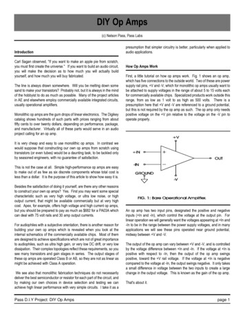
DIY Op Amps(c) Nelson Pass, Pass LabsIntroductionCarl Sagan observed, "If you want to make an apple pie from scratch,you must first create the universe." If you want to build an audio circuit,you will make the decision as to how much you will actually buildyourself, and how much you will buy fabricated.The line is always drawn somewhere. Will you be melting down somesand to make your transistors? Probably not, but it is always in the mindof the hobbyist to do as much as possible. Many of the project articlesin AE and elsewhere employ commercially available integrated circuits,usually operational amplifiers.Monolithic op amps are the gum drops of linear electronics. The Digikeycatalog shows hundreds of such parts with prices ranging from aboutfifty cents to over twenty dollars, depending on performance, package,and manufacturer. Virtually all of these parts would serve in an audioproject calling for an op amp.presumption that simpler circuitry is better, particularly when applied toaudio applications.How Op Amps WorkFirst, a little tutorial on how op amps work. Fig. 1 shows an op amp,which has five connections to the outside world. Two of these are powersupply rail pins, V and -V, which for monolithic op amps usually want tobe attached to supply voltages in the range of about 5 to 15 volts eachfor commercially available chips. Specialized products work outside thisrange, from as low as 1 volt to as high as 500 volts. There is apresumption here that V and -V are referenced to a ground potential,but this is not required by the op amp as such. The op amp only needspositive voltage on the V pin relative to the voltage on the -V pin tooperate properly.It is very cheap and easy to use monolithic op amps. In contrast wewould suppose that constructing our own op amps from scratch usingtransistors (or even tubes) would be a daunting task, to be tackled onlyby seasoned engineers, with no guarantee of satisfaction.This is not the case at all. Simple high-performance op amps are easyto make out of as few as six discrete components whose total cost isless than a dollar. It is the purpose of this article to show how easy it is.Besides the satisfaction of doing it yourself, are there any other reasonsto construct your own op amps? Yes. First you may want some specialcharacteristic such as very high voltage, or ultra low noise, or highoutput current, that might be available commercially but at very highcost. Apex, for example, offers high voltage and high current op amps,but you should be prepared to pay as much as 682 for a PA03A whichcan deal with 75 volt rails and 30 amp output currents.For audiophiles with a subjective orientation, there is another reason forbuilding your own op amps which is revealed when you look at theinternal schematics of the commercially available chips. Most of themare designed to achieve specifications which are not of great importanceto audiophiles, such as ultra high gain, or very low DC drift, or very lowdissipation. Their complex topologies reflect these requirements, so yousee many transistors and gain stages in series. The output stages ofthese op amps are operated Class B or AB, so they are not as linear asmight be achieved with Class A operation.We see also that monolithic fabrication techniques do not necessarilydeliver the best semiconductor or resistor for each part of the circuit, andby making our own choices in device selection and testing we canachieve high linear performance with very simple circuits. I take it as aPass D.I.Y Project: DIY Op AmpsAn op amp has two input pins, designated the positive and negativeinputs ( In and -In), which control the voltage at the output pin. Forlinear operation we will generally want the voltages appearing at In and-In to be in the range between the power supply voltages, and in manyapplications we will see these pins operated near ground potential,midway between V and -V.The output of the op amp can vary between V and -V, and is controlledby the voltage difference between In and -In. If the voltage at In ispositive with respect to -In, then the output of the op amp swingspositive, toward the V rail voltage. If the voltage at In is negativecompared to the voltage at -In, the output swings negative. It only takesa small difference in voltage between the two inputs to create a largechange in the output voltage. This is known as the gain of the op amp.That's about it.page 1
The Role of FeedbackOf course there's really quite a bit more, and most of it involves theconcept of feedback. The control pins of the op amp are usually sosensitive that it is nearly impossible to keep the output voltage in theuseful (linear) range between the supply rails without some method ofcontrolling the system, and this method is feedback. Feedback works tokeep the differential input voltage (the voltage difference between Inand -In) very small, which keep the output in the linear range.If we want gain, we simply have to fool the negative input into thinkingthat the output is smaller than it actually is, as in Fig. 3, where thenegative input sees the output voltage after a voltage dividing network.The dividing network reduces the voltage by R2/(R1 R2). As a result,the op amp delivers an output that is a multiple of the input, where thegain is given by the inverse of the divider: (R1 R2)/R2. As an example,if R1 is 9 KOhm and R2 is 1 KOhm, then the gain would be 10, and a 1volt input at In would result in a 10 volt output.Another simple feedback connection allows the negative input to bedriven by the signal source, resulting in an inverted output voltage. Fig.4 shows such a connection, with the gain given by the formula R1/R2.Again following the logic of the op amp input pins, a positive signal fromthe source will drive the negative input so that the output of the op ampgoes very negative, and this feeds back around through R1, greatlyreducing the positive voltage. Because in this case the positive inputhas been tied to ground, the op amp works to keep the negative inputvery close to ground potential. As a result, this circuit is useful as amixer, since the negative input can be driven by multiple sources, eachwith their own resistor, and they won't interact, since the negative inputis held to ground potential, a "virtual ground", by the feedback loop of theop amp.We do this by communicating between the negative input and the outputof the op amp. The easiest example of this is the simple voltage followerof Fig. 2. In this circuit, the negative input is connected directly to theoutput, with the result being that the output of the op amp matches thesignal presented to the positive input.Following the logic of an op amp's control pins, we observe that if thevoltage from a signal source driving the positive input were to gopositive, the output of the op amp would start to go very positive. Butthe output of the op amp being connected to the negative input wouldcause it to go positive also, and it will not want to go more positive thanthe positive input, or else the output would head off in the negativedirection. Instead it will come very close to the voltage at the positiveinput, with just enough difference to allow the op amp's output to trackthe input.A simple rule of thumb about open loop gain and feedback is that thedifference between the open loop gain and the actual output gain is howmuch feedback has been applied. If the open loop gain is 60 dB(X1000) and the actual output gain is 20 dB (X10), then 40 dB (X100) offeedback has been applied.Certainly there is more to know about feedback, and the above isintended as enough to start playing. There are a number of excellentsources on op amps and feedback, but my favorites come from NationalSemiconductor's Linear Application Notes ( Digikey (800) 344 4539,order # 9245B-ND ), where 30 years ago I learned most of what I knowon the subject. Of particular interest is Bob Widlar's 1968 piece"Monolithic Operational Amplifiers - The Universal Linear Component",as the legendary Widlar is widely regarded as the fountainhead ofmonolithic op amp design.Pass D.I.Y Project: DIY Op Ampspage 2
Gain Devices: A Short TutorialOp amps are constructed of gain devices and resistors. The gaindevices we will deal with are three terminal devices that are used tocontrol electron flow in a circuit. Current flows through two conductingpins, governed by a third control pin. The voltage or current applied tothe control pin is taken relative to one of the other pins. In a Fet or aTube, the current flowing through the main connections is a function ofthe control pin voltage relative to one of the other pins, and in a Bipolartransistor, it is a function of the current through the control pin.In a Fet the control pin is called the Gate. In a Tube it is called the Grid.In a Bipolar transistor it is called the Base. The control exerted by eachof these control pins operates relative to one of the other pins in thedevice. In the Fet the Gate operates relative to the Source pin,controlling the current between the Source and the other pin, the Drain.In a Tube, the current flows from Plate to Cathode, and is controlled bythe voltage between the Grid and the Cathode. In a Bipolar transistor,the current flows from Collector to Emitter, and is controlled by thecurrent between the Base and Emitter.Fig. 5 shows these three types of devices, and the voltage and currentrelationships of their pins. Fig. 5A and 5B show an "N channel" Fet andan NPN transistor, and you will note that 5D and 5E show a "P channel"Fet and a PNP transistor. These "P" types are like the "N" types, buthave the current and voltages reversed. The availability of these"negative" versions of the parts is very convenient, and is an advantageover tubes, which have only "N" type polarity.For the purpose of simplifying this discussion, I will now refer to Mosfets,at the end of which we will make note of the major differences betweenthese types of devices.As noted, the current flowing through the main pins of the device is afunction of the voltage between the control pin and one of the other pins,and in the case of a Mosfet, this would be between the Gate and Sourcepins. As the voltage on the Gate becomes positive relative to thevoltage on the Source, current will begin to flow from the Drain to theSource. This is how the device amplifies electrical signals. The morepositive the voltage between the Gate and Source, the more currentfrom the Drain to Source.Pass D.I.Y Project: DIY Op AmpsIt is of interest to know at what rate the current will change respectingthe Gate-to- Source voltage. This Fig. is called the transconductance,and tells you how much change in current to expect for a change in Gatevoltage. It is often expressed as mhos (the opposite of ohm), because itdescribes an inverse of resistance. An ohm is volts divided by amps, anda mho is amps divided by volts, so that transconductance is seen as thechange of current for a change of control voltage. A device having onemho transconductance will increase its current by 1A for each additionalvolt on the gate. Most signal Mosfets have transconductance on theorder of .1 or so, and power Mosfets over have figures on the order of10, so that they conduct 10 amps per control volt.Most N channel Mosfets will begin to conduct somewhere with a gate tosource voltage around 3 to 4 volts, and so in linear circuits you willusually see this range of DC voltage between the Gate and Source pins.Naturally, all this assumes that the Drain of the Mosfet has positivevoltage applied to it relative to the Source, otherwise the current won'tflow. In much in the same way you can adjust the knob on a waterfaucet, but you won't get flow unless there is pressure.For a P channel Mosfet, the action is the same, but the voltages andcurrent flows are reversed. The P channel Mosfet will begin conductingwhen the Gate to Source voltage reaches around -3 to -4 volts.The gain devices we will consider have three pins, and there are onlythree ways to use them. Fig. 6 shows the three ways to use an Nchannel Mosfet, each referred to by a "common pin" name, which is thatdevice pin which does not carry signal voltage. The first use is commonDrain operation, also known as follower operation. It has current gain butno voltage gain. The input signal is presented at the Gate, and theoutput comes from the Source as nearly the same as the input voltage,but shifted - 4 volts DC or so and with a lot more current capacity. Thesecond is common-Source operation, in which we have both voltageand current gain. The input is at the Gate, and a phase inverted outputsignal appears at the Drain. The load for the transistor is shown as aresistor here, but can be some other, possibly more complex, load.The third way to use a Mosfet is with common-Gate operation, whichhas voltage gain but no current gain. Input appears at the Source;output appears at the Drain. This connection is most popularly used toform Cascode operation, in which a common-Gate device shields apage 3
common-Source device.The same principles that govern the use of Mosfets applies to othertypes of gain devices, but with the following differences:In JFets, the Gate to Source voltage has a much lower DC value, usuallynegative, on the order of -1 volt or so. Also, JFets generally have lowertransconductance than Mosfets, often on the order of .01 or so.Tubes require much higher voltages, often greater than 100 volts Plateto Cathode, than solid state devices, and generally conduct less current.For linear operation of a Triode like a 12AX7, the Grid to Cathode DCvoltage is a few volts negative, and we see a transconductance on theorder of .003, or about 3 milliAmps of current for each control volt.Bipolar transistors have what you would think of as a very hightransconductance Fig., but that is not an appropriate way of looking atthem because the current through the device is a function of the currentthrough the control pin. The Base pin voltage relative to the Emitter pinis a relatively constant Fig. on the order of .7 volts, but the current fromthe Collector to Emitter is a multiple of the Base to Emitter current. ThisFig., ranging from less than 10 to as high as 1000, is known as thecurrent gain, or beta, of the Bipolar transistor.OK, so now we know enough about gain devices to be dangerous, butkeep in mind that there are many little details about the characteristicsof the various gain devices, details which are generally spelled out in thedata sheets and which are worth studying.So let's build some op amps.The first step is to construct an input stage known as a differential pair:two transistors with their Sources tied together, and fed current at thatconnection, as shown in Fig. 7. In this case, current is fed through acurrent source attached to a negative supply voltage. Two inputs areavailable at the Gates, as are two outputs at the Drains, which thencommunicate through loads to the positive supply. For simplicity, thecurrent sources of Fig. 7 are provided by resistors, although a variety ofimpedance components could be employed. Among the alternatives forthese impedances are active constant current sources, where thecurrent will not vary with the voltage. In Fig. 7, I1 is the current sourcedto the differential pair which is then evenly divided up into I2 and I3.The Drains present equal but inverted outputs, which represent thedifference between the inputs. If both inputs see the same signal, thenthat signal ideally does not appear at the outputs. It is a differentialamplifier, which means any differences in the input signals at the gatesare amplified, and common signal is rejected. For this reason, it isextremely useful as the input stage for an amplifier, because you canconnect an input signal to one gate and use the other gate to watch theamplifier output.This output watching is called feedback. The differential pair is used tocompare input and output, and by amplifying their differences it is usedto correct for errors at the output.Depending on the choice of devices, voltages, and resistance values,the differential pair of Fig. 7 will have a certain amount of voltage gain,which in this case is around 20 dB (X10). For some purposes, this mightbe enough, as in the AE projects "Son of Zen" and "Bride of Son of Zen"in which a power amplifier and accompanying preamplifier are simplydifferential pairs, nothing more.Step 1: Constructing a Differential InputStep 2: A Second Gain StageThe key to an operational amplifier is the two gain devices that form thedifferential input. You can build a functional op amp from this alone,although more typically it will be followed by one or more additionalstages.Pass D.I.Y Project: DIY Op AmpsMost of the time, though, we want more open loop voltage gain thanprovided by just a differential pair so we can have some left over forfeedback correction. Also, it would be convenient to arrange thecircuitry so that the output swings the full voltage of the supplies, whichpage 4
the differential pair is not useful. A second gain stage becomes anecessity for this.Fig. 8 shows the application of a second gain stage to the circuit of Fig.7. We have added a P channel Mosfet operating in common Sourcemode and driving a resistor R3 connected to the negative supply. R2 ischosen to give about 3 volts DC to drive the Gate to Source voltage ofQ3. This value must often be adjusted to make I2 and I3 equal andcreate lower offset input voltage for the op amp, since not every Pchannel Mosfet will want exactly 3 volts of drive.2 Volts output, the distortion is flat from 20 Hz to 20 KHz. The circuit of8b is set up for a balanced input, but is easily converted to single inputby connecting either of the inputs to ground. Of course you can replacethese four resistors with some other network that performs a differenttask.We can easily create some other versions of this circuit using othertypes of gain devices. Fig. 10 shows this circuit rendered with BipolarThis is a complete and functional op amp. It has an input CMRR ofabout -42 dB, and an open loop gain greater than 50 dB. It will swingtransistors rather than Mosfets. It has a higher open loop gain, andyields lower distortion and better CMRR figures than the Mosfet circuit.The distortion curve for this circuit is given in Fig. 11.20 volts RMS at its output with low distortion, with a slew rate around 80Volts/microSecond.Resistors Ra, Rb, Rc, and Rd are not part of the op amp itself. They arean "external" network for input and feedback that make this particular opamp into a linear differential amplifier. Ra is set equal to Rb, and Rc isequal to Rd, and the gain of the amplifier is Rc/Ra. Fig. 9 shows thedistortion curve of this particular circuit at 1 KHz between .1 and 20 voltsoutput. Below 1 volt, noise dominates the distortion curve. Measured atPass D.I.Y Project: DIY Op AmpsAgain this is a functional audio gain block that you can build and use.Note that the PNP transistor 2N4250, has an emitter resistor to lower theopen loop gain a bit and enhance stability, and that capacitor C1 isemployed to frequency stabilize the circuit when operated closed loop.With Bipolar transistors there is less need to match devices on thedifferential pair as long as the current gain figures are fairly high. In thiscase, the MPSA18's have betas of several hundred, as does thepage 5
gain for audio applications, but often not enough current gain to drivelower impedance loads. We can achieve more current gain by addinganother gain stage operated in common Drain, or follower, mode, whichgives us current gain but not voltage gain.Fig. 13 shows the addition of voltage followers for the circuits of Figs 8and 10. The open loop output impedance of Figs. 8 and 10 are simplythe values of the resistors attached to the negative rail, which is 3Kohms in Fig. 8 and 6.8 Kohms in Fig. 10. With a closed loop, thesevalues are reduced by feedback, so that 40 dB of feedback would resultin functional output impedance of these resistors divided by 100.2N4250. The Base to Emitter voltages of these devices is consistent at.65 Volts or so, whereas Fets and Tubes are found to have much greaterrelative differences, and benefit more from matching. You can useBipolar devices with less gain, commonly around 100 or so, but theperformance will decline slightly.Fig. 12 shows what you might do to create a Triode op amp using12AX7's. I did not build this device, but I believe it would workadequately for some audio applications, and would offer true DCamplification. The trick of getting the level shifting to properly bias theparallel output tubes lies in creating a DC voltage source interposedbetween the output plate of the differential pair and the grids of thefollowers. This can be provided by external DC supplies, such asbatteries. This particular circuit would not offer much open loop gain orspectacular performance, but it does illustrate the potential foroperational amplifiers without P type gain devices.The addition of a follower to Fig. 8 results in an open loop outputimpedance equal to the inverse of the transconductance, resulting inabout 20 ohms or so. For the Bipolar device of Fig. 10, it would be theoriginal 6.8 Kohms divided by the current gain (beta) of the transistor,also resulting in about 20 ohms or so.The follower not only gives a lower output impedance, but makes theperformance of the op amp less dependent on the load impedance. Ifyou want to drive a lower impedance load, particularly a loudspeaker,you will want some current gain, and very often you will want this thirdstage.Keep in mind that these issues heavily depend on the requirements ofthe circuit and the type of device. As a practical matter, Mosfets give thebest combination of characteristics for performance from the mostsimple power circuits at higher currents, but JFets are superior at lowpower levels for noise and input impedance. Bipolar signal devices givevery high gain in low impedance circuits, and so they often measurebetter in cases where the source impedance is low.Step 4: More PerformanceConstant Current SourcesSo far we have built these op amps using resistors to set up the currents(bias) through the gain devices. This is a simple and linear way to do it,but often we want to bias the gain devices with currents that do not varywith voltage, as they will with resistors. These are called constantcurrent sources. Constant current sources operate so as to pass aconstant current over a wide range of voltages, and in so doing, they canimprove the environment in which the gain devices work. Fig. 14 showsthe Mosfet and Bipolar op amps of Fig. 13 where the resistors have beenreplaced by constant current sources.Step 3: Still More GainThe second gain stage of Fig. 8 was created by a P channel deviceoperated in common Source mode, which offers both voltage andcurrent gain. Routinely, this second stage gives us adequate voltagePass D.I.Y Project: DIY Op AmpsFig. 15a shows the details of these current sources as made withMosfets. It takes about 3.5 volts to bias up the Gate to Source pins of aMosfet, so we create a voltage reference using the Zener diode andresistor. The resistor runs a small amount of current through the Zenerdiode, which creates a constant voltage. We use this voltage, 9.1 volts,to drive the Gate of the Mosfet. The Gate to Source requirements willeat up 3.5 volts of this, leaving 5.5 volts across the Source resistor,which causes the Drain of the Mosfet to source current as determinedby 5.5/R. The 221 ohm resistor in series with the Gate preventsparasitic oscillation in the Mosfet, and is generally essential. Thispage 6
current source works quite well, and can be easily used at high voltagesand high currents. It tends to be noisy at low level usage, but this canbe improved by placing a capacitor across the Zener diode, which is amajor contributor to the random noise.Fig. 15b shows the current sources as made with Bipolar devices. Inthis case, the bipolar transistor forming the current source is driven bybias voltage created using a pair of diodes. The diodes drive the baseof the transistor with about 1.3 volts, and the Base to Emitter junctiondrops about half of that, leaving about .65 volts left over to determine thecurrent through the Emitter resistor of the current source. The currentcoming out of the Collector will be relatively constant at .65/R.Fig. 15c shows current sources formed from JFets. JFets normally havea negative gate voltage, and so they conveniently form a self-biasedcurrent source as shown. For an N channel device like the 2SK170, thegate voltage is about -.3 volts, so we simply set the source resistorvalue for current determined by .3/R. As shown, the current sources areset for 4 milliAmps. Besides simplicity, JFets have the advantage ofbeing very low noise. On the down side, they are limited in their abilityto handle high voltages and dissipate wattage.Pass D.I.Y Project: DIY Op AmpsThe choice of which device to use for current sources is up to you.There is not requirement that you use Mosfets current sources in theMosfet op amp, nor is there are requirements that you must use currentsources everywhere in the circuit. You are free to use current sourceswhere you choose, or not, depending on the results you want.The willingness to experiment is very important to getting the results youwant. You can evaluate performance subjectively or objectively, but youshould always be prepared to try things out.Using a constant current source to bias the differential pair (I1) isprobably the most key improvement. It has the advantage that it doesnot raise the open loop gain, but dramatically improves the power supplyrejection (PSRR), making the performance independent of supplyfluctuation and noise. It also greatly improves the common moderejection (CMRR) of the input stage, typically by a factor of 20 to 30 dB.The second most useful spot for a constant current source is where thesecond gain stage is loaded (I4). This raises the gain of this stage,lowers the distortion, and again improves the power supply rejection.page 7
I have not shown current sourcing where R2 is replaced by a constantcurrent source, and this is a technique often used in monolithic op ampsas it increases the gain of the differential pair and raises the open loopgain of the op amp, sometimes dramatically. Sometimes it is necessarywhen you need very high gain, such as in phono stages, but it is oftenmore trouble to implement than it is worth in line level applications. Therequirement for low voltage across this current source makes it a littlemore difficult, and we will leave it as a future advanced exercise.We note on the distortion curves of our op amps that the distortion curveis seen to rise as the output goes below a volt or so. This is mostly dueto random noise in the differential input devices. For the Mosfet circuitof Fig. 8, this amounts to about 10 microVolts of noise. For the Bipolarcircuit of Fig. 10 it is about 2 microVolts.Current sourcing the third output follower stage (I5) gives some linearityimprovement and improves the efficiency and PSRR of a single-endedClass A output stage, but is often not essential to the performance of aline level stage with a regulated supply.Lowering the NoisePart of having low noise is either having high power supply rejection(PSRR) or a quiet power supply. It is not difficult to use quiet currentsources or a quiet power supply or both. After that, the noise willdepend heavily on the quality of the input transistors.For even lower noise, it is possible to use low noise JFets as thedifferential pair, giving random input noise on the order of .4 microVolts.Fig. 16 shows the circuit of Fig. 8 but with 2SK389 dual low noise JFetsdropped in. The distortion and noise at low levels drops by an order ofmagnitude, but the performance at higher levels is nearly identical, asseen in Fig. 17.MiscellaneousAll of the example op amps presented here have used 32 Volt rails,which represents a reasonably good trade off between performance ofthe simple circuits and the ratings of the devices. We can get someinteresting improvements at higher voltages with higher voltage devicesand use of cascode operation, but that is beyond the scope of what weare trying to accomplish here.Projects using monolithic op amps routinely have plus and minus 15 voltrails, as this represents the supply ratings of many devices. You mayPass D.I.Y Project: DIY Op Ampspage 8
find yourself wanting to transplant some of our example circuits intothese projects, in which case you have the choice of either creatinghigher voltage supplies or adjusting the biasing of the op amps.As you raise the supply rails, the values bias resistors R1, R3, and R4are increased to give the same current, and at higher values they lookmore like constant current sources to a given level of signal. This is avery easy way to improve the performance without introducing moreparts.If you choose to use the lower 15 Volt rails of an existing project, you willwant to adjust the resistors which determine I1, I4, and I5. As a practicalmatter, you can simply halve their values to get the same amount ofcurrent, and the reduction in performance will be nominal, but not likelya real problem. You will not be halving the value of R2 as long as I1remains the same.None of these bias values are critical; in fact I pulled them out of the airwithout any attempt to optimize the performance. If you play around withthe various values of resistance and current, you may find theperformance improved. If you have a distortion analyzer, it is perfectlyacceptable to tweak the values for a lower distortion number.It is highly probable that you will want to adjust the resistors in aparticular application to get low DC offset at the output, so don't be afraidto play around. Remember, none of these parts costs as much as adollar.Likewise, feel free to substitute different kinds of gain devices in an
in AE and elsewhere employ commercially available integrated circuits, usually operational amplifiers. Monolithic op amps are the gum drops of linear electronics. The Digikey catalog shows hundreds of such parts with prices ranging from about fifty cents to over twenty doll