Transcription
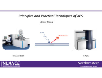
Principles and Practical Techniques of XPSXinqi ChenESCALAB 250XiK Alpha
Outline1. Brief introduction of the shared instruments in Keck‐II2. XPS basic principles and instrumentation3. Various characterization techniques with XPSQuestions
FT‐IRSample:Mode: Bruker Lumos IR MicroscopeTransmissionATRDRIFT PowderFilmSolutionGelMicrometer spotThermo Nicolet iS50 FT‐IR spectrometer
Surface ProfilerOptical profilometer(3D optical microscope)Stylus profilometer
Ellipsometer
ION TOF M6 TOF SIMS High lateral resolution ( 50 nm)with the new Nanoprobe 50. From nm to µm – DSC, the high‐performance work horse forinorganic depth profiling with O2 andCs. Quantitative depth profiling inMCs Mode Gas Cluster Ion Source ‐ The bestsolution for organic depth profiling Focused ion beam (FIB) – crosssection analysis Sample Heating and Cooling
XPS BackgroundXPS technique is based on Einstein’s discovery of the photoelectric effect in1905 The concept of photons was used to describe the ejection ofelectrons from a surface when photons were impinged upon it. 1921 Nobel Prize in Physics "for his discovery of the law of thephotoelectric effect"During the mid 1960’s Dr. Kai Siegbahn and his research group developed the XPS technique.– Electron Spectroscopy for Chemical Analysis (ESCA)– In 1981, Dr. Siegbahn was awarded the Nobel Prize in Physics for thedevelopment of the XPS technique– Manne Siegbahn (Kai’s father) was awarded the Nobel Prize in Physics in1924 "for his discoveries and research in the field of X‐ray spectroscopy".
Core ElectronEquationKE hv-BE-ØBE hv-KE-Ø
Basic Components of XPS Instrumentation UHV system (i.e., 10‐9 torr):– Ultra‐high vacuum keeps surfaces clean– Allows longer photoelectron path lengthX‐ray source:– Typically Al Kα radiation (1486.6 eV)– Monochromated using quartz crystalLens, energy analyser & detectorLow energy electron flood gun:– Low energy e‐ (plus Ar )– Analysis of insulating samplesIon gun:– Typically noble gas ions (monatomic or clusters)– Sample cleaning– Depth profilingDigital CamerasHemispherical ElectronEnergy AnalyzerMulti‐ChannelDetectorArgonIon GunElectronTransfer LensMonochromatorArgon Ion/ElectronFlood GunSampleStageAl Kα X‐raySource
X‐Rays and the ElectronsX-RayElectron without collisionElectron with collisionThe noise signal comes from theelectrons that collide with otherelectrons of different layers. Thecollisions cause a decrease in energy ofthe electron and it no longer willcontribute to the characteristic energyof the element.
103 eV99 eV
XPS Spectra: 10% Pd/Activated Carbon Catalyst XPS survey spectra (left) provide qualitative and quantitative elemental surface information. High resolution XPS spectra (right) provide chemical state surface information.Surface Composition (Atomic %)C ‐ 91.6%O ‐ 5.5%Na ‐ 1.6%Cl ‐ 0.1%Pd ‐ 1.2%Pd 3d5/2C 1sPd 3d3/2IntensityIntensityPd 3d XPS spectra have twospin‐orbit split peaks (i.e., Pd3d5/2 and 3d3/2) for eachchemical species present.Pd MNNC KLLO 1sO KLLPd 3dPd 3pNa 1sCl 2pNa KLL1300 1200 1100 1000900800700600Binding Energy (eV)5004003002001000350340Binding Energy (eV)330
Peak Fit for the Pd 3d XPS Spectrum: 10% Pd/Activated Carbon CatalystPd 3d3/2 Pd MetalPd 3d5/2 PdOPd 3d5/2 PdO2Pd 3d5/2 Pd MetalIntensityPd 3d3/2 PdOPd Species Detected by XPS:Pd Metal ( 15%)PdO ( 80%)PdO2 ( 5%)Pd 3d3/2 PdO2Pd 3d Plasmon Loss350340Binding Energy (eV)330
AgSi
Variation in Sampling Depth with Angle‐Resolved XPS (ARXPS)SiCompare-21.10E 051.00E 059.00E 04Si4 8.00E 04Counts / s7.00E 046.00E 04Angle 205.00E 044.00E 043.00E 042.00E 04Angle 901.00E 040.00E 00110109108107106105104103102101100Binding Energy (eV)Sampling depth d 3 sinΘΘ electron take‐off angle IMFPNative SiO2 on Silicon9998979695
Heating and Cooling in Analysis ChamberSample plate temperaturerange: ‐170C to 300C
Summary of XPS Analysis Capabilities1.Provides quantitative elemental and chemical state information for all elements except H and He.2.Detection limit is 0.05‐0.1 atomic % for most elements.3.Sampling depth 10 nm.4.Can be used for point analysis, line scans, and area analysis (mapping and imaging).5.Can provide in‐depth analysis by AR‐XPS (1‐10 nm) or ion sputter depth profiling (sputtered depths of 10 µm ormore now possible).6.Can be used for conductive and insulating solid samples, e.g., metals, metal oxides, catalysts, ceramics, coatings,multi‐layer thin films, polymers etc.7.Samples can be fibers, foil, particulate, powder, rods, sheet, thin film, etc. In general, no special samplepreparation is required.8.Samples must be compatible with ultrahigh vacuum ( 10‐8 torr or lower) and stable under Al Kα X‐raybombardment.
Pros Quantitative elemental compositionChemical bonding informationSurface sensitiveAll solid materials including insulator,semiconductor, and metals Analysis is fast and easyCons Poor lateral resolution UHV compatible
Avantage software is free downloadable. XPS Knowledge View is helpful.
Detailed data process procedure isavailable in Avantage help file.
Mar 18, 2021 · Bruker Lumos IR Microscope Thermo Nicolet iS50 FT‐IR spectrometer Mode: Transmission ATR DRIFT Sample: Powder Film Solution Gel Micrometer spot. Surface Profiler Optical profilometer (3D optical micro