Transcription
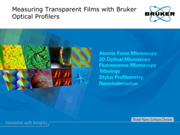
Measuring Transparent Films with BrukerOptical Profilers
Outline Introductions Review of Vertical Scanning Interferometry (VSI) Extending VSI to Measure Films Film Measurement – Thick vs. Thin Films Some Film Results Capabilities and Limitations Summary & Survey5/20/20162
Introductions – About UsBruker Tribology, Stylus and OpticalMetrology Technology Leadership 60 Patents 4 R&D 100 Awards 6 Photonics Circle ofExcellence Awards Manufacturing Excellence Lean, six sigma-based process Right-sized operations Rapid production rampcapabilityBruker NSD TSOM is part of Bruker Nano Group, a division of Bruker5/20/20163
Introductions – About MeSpeaker Adam Wise, Ph.D.Field Applications / Systems SpecialistAdam.Wise@Bruker.Com Background in OpticalInstrumentation / Physical Chemistry Formerly in Organic Photovoltaic R&D– thin polymer film measurementscritical5/20/20164
Who Will Benefit? Optical Profiler users looking to measure transparent insulatingfilms from 100nm to 100um Users who want to measure film thickness, surface finish,topography, coverage, holes in films Those looking to extend into film measurements withoutpurchasing an imaging ellipsometer5/20/20165
Key ValueAfter the Presentation you will Know how to set up and run film measurements Understand the fundamental capabilities and limitations offilm measurements via Optical Profiler Reasonably predict whether the Vision64 films package is agood match for your samples5/20/20166
White Light InterferometryCamera Highly accurate surface measurementCCD Fringes measure difference in path lengthbetween reference and signal armReferenceMirrorLReference Many overlapping interference patternswith different λ only match up when ΔL 0Light SourceLSignal Fringes only when length of “reference”arm length of “signal” armSampleFringes for:blue lightgreen lightyellow lightred light5/20/2016WLI Envelope width 2*λ2/Δλ 535*535/150 2 μm7
Vertical Scanning Interferometry (VSI)Quick Review Builds up map ofsurface by sweepingoptics through Z Center of mass (COM)of each camera pixel’sfringe envelopedetermines heightFocus5/20/20168
Films – Multiple ReflectionsFilmSubstrate Transparent film on thesurface means additionalreflections Reflected beams interferewith each other and withreference beam How does the softwarehandle this?5/20/20169
Film ThicknessIntensity at detector“Thick”Thickness 2μm“Thin”Thickness 2μmChange in Signal Path LengthWith “thick” films ( 2 μm), modulation envelopes are separable “Thin” films ( 2 um), modulation envelopes overlap Different measurement strategies – both handled by 1 add-on5/20/201610
Vision64 Films Package Software-only upgrade available for all Contour-GT models Adds new measurement mode to measurement setup Works through standard Vision64 GUI Allows measurement of films 100nm-100um Functionality broken down by thickness range – 2 modes5/20/201611
Thick Film Measurement Capability available as part of film option Knowledge of the group index (ng) of refraction is needed For films 2 μm up to a practical limit of 150 μm Maximum film thickness is limited by dispersionOptical Path DifferenceFilm Surface𝑻𝒉𝒊𝒄𝒌𝒏𝒆𝒔𝒔 𝒏𝒈Substrate5/20/201612
Thick Film MeasurementMeasurement Setup Flow Setup takes 1 min Subsequent measurements take a few secondsMeasure orlook up elopeThresholdsMakeMeasurement13
Thick Film MeasurementGroup index and optical thickness Optical propertiescharacterized by grouprefractive index ng ng from publishedvalues, or by opticalmeasurement ofknown film thickness Optical thickness ng*physical thickness5/20/2016Film SurfaceOPTICALFilmThicknessFilm ThicknessFilm/SubstrateInterface14
Thick Film MeasurementMeasurement Parameters Similar to standard VSI setup Choose backscan/length to fit optical thickness of film Define treatment of single-surface data, e.g. uncoated substrate5/20/201615
Thick Film MeasurementEnvelope Thresholds Allows user to set s/n thresholds for film & substrate “Set Env. Thresholds” button pops up wizard Interactive GUI based on trial data5/20/201616
Thin Film MeasurementMeasurement Setup Flow Setup takes 5 min Subsequent measurements take a few seconds Requires reference sample – uncoated substrate –to measure system responseChooseMeasurementParameters5/20/2016Build Modelwith ReferenceSampleCalibrateAgainstKnown FilmSet Boundsfor ThicknessResults(optional)Measure17
Thin Film MeasurementsMethod Basics Signals overlap from surfaces– cannot separate film andsubstrate envelopes viacenter of mass (COM) Use FFT to compute A, φ forreflected electric field Compare measured signal tomodels generated for variousmaterials, thickness5/20/201618
Films – Build Model Model build takes approximately 30seconds to one minute with a goodclean sample and known materials Vision provides a list of knownmaterials New materials can be added as a*.mat file for Vision (wavelength,index, absorption (for now, α 0) Model build with sample which is sameas film substrate, but with no film forbest results5/20/201619
Films – Calibrate ThicknessRequires film sample of target material, known T Thickness calibration requires film of same materialon same substrate Need to then select proper film model in order tomeasure5/20/201620
Film Model Generation andDetails5/20/201621
Setup and Model GenerationDetails of successful model generation below5/20/201622
Predict Results – Two WaysMerit Function or Nominal Thickness Target “Use Nominal Value”- Bound thicknessresult with nominalvalue tolerance “Use Merit Function”– find global meritfunction minimum, orwithin search range5/20/201623
Merit Function GraphCompute thickness, unknown target T (use caution) Merit functionshows map ofmost likely modelresults Merit function isperiodic – mustset bounds ifglobal minimum isunrealistic5/20/201624
Target Nominal ThicknessUser inputs nominal T (with tolerance range) Nature of the filmdictates lobespacing in themodel generation Tolerance rangegenerally 100nmgenerally OK5/20/201625
Results Next section shows a few resultswith different samples Al2O3 (alumina) on Si Silicate (SiyOx)- on Si with voids/crackswith color camera5/20/201626
Al2O3 on Si – 500nm FilmResults images – thickness5/20/201627
Verification of Thin FilmMeasurement (Dektak, Optical) Silicate FilmMap this area –easy to locate on3D profilerExample - Cu/AlSilicate mineral5/20/201628
Dektak MapThickness varies from 1.2 um to 100 nm750 um x 750 um x 1 um line spacing5/20/201629
ContourGT-I Film SoftwareGood agreement compared to tactile result5/20/201630
Results Best PracticesSome tips to consider Optimize results by. Ensure system is properly set up (calibrations,vibration isolation, etc.) Use same scanner position for sample andcalibration and references Use careful null of fringes Use white light, lower magnification like 5x or10x as possible Enter a target thickness with tolerancewhenever possible Use similar intensity to model5/20/201631
Thin Films - Limitations Roughness – accurate measurement requires “PSI-smooth”samples RMS roughness 30nm Known Optical Properties – must know dielectric function, mustbe insulating Thickness – 100nm, may need to know approximate thickness Need reference - Must have reference sample (bare substrate) Uniform Optical Properties – refractive index must be uniformover area to be measured5/20/201632
Thick Films - Limitations Magnification – Generally 20X, material / thicknessdependent Thickness – 2μm-150μm Known Optical Properties – must know group refractive index ng Uniform Optical Properties – refractive index must be uniformover area to be measured5/20/201633
Conclusions Thin films add-on for Bruker optical profilers extends thecapability of optical profilers Interface & use already familiar to ContourGT users Accurate thickness measurements require knowledge ofsamples properties and understanding of capabilities /limitationsQuestions and Survey5/20/201634
Bruker Tribology, Stylus and Optical Metrology 5/20/2016 3 Technology Leadership 60 Patents 4 R&D 100 Awards 6 Photonics Circle of Excellence Awards Manufacturing Excellence Lean, six sigma-based